Clamp Cap
Clamp Gate Input
Ground
+Vcc
Video Output
NC
Clamp Input (-)
Clamp Input (+)
Ground
4707 Dey Road Liverpool, N.Y. 13088
M.S.KENNEDY CORP.
(315) 701-6751
FEATURES:
230 MHz Video Bandwidth With Vout=4Vpp
Transition Times Less Than 2.0nS With Vout=4Vpp
0 To 4 Volt High Input Impedance DC Drive Control With ±3dB Range
0 To 4 Volt High Input Impedance DC Contrast Control With 40dB Range
Externally Gated Comparator for Brightness Control
Simple To Parallel For RGB Color Tracking
0.5V to 9.0V Output Voltage Swing Capability
On Board Accurate Reference Voltage Generator
Available Fully Screened to MIL-PRF-38534
WIDE BANDWIDTH VIDEO
AMPLIFIER SYSTEM
MIL-PRF-38534 CERTIFIED
620
1
2
3
4
5
6
7
8
9
Control Output (+)
Attn. Input (+)
Attn. Input (-)
Control Output (-)
Ground
Video Input
Contrast Control Input
Drive Control Input
Vref Output
PIN-OUT INFORMATION
10
11
12
13
14
15
16
17
18
Wideband Amplifier With Gain
and DC Offset Control
High Resolution CRT Monitor
Ultra High Performance Video Processing
TYPICAL APPLICATIONS
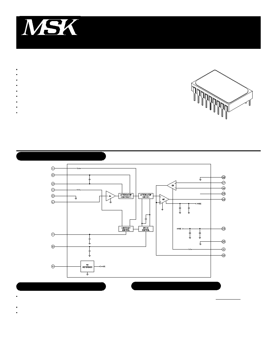
EQUIVALENT SCHEMATIC
The MSK 620 is a very high frequency video amplifier system capable of driving displays with resolutions up to 1664 x
1200. Brightness is controlled with a gated differential input black level clamp comparator. There are also DC inputs
available for contrast control and drive control. All DC control inputs operate over a 0V to 4V input range and feature high
impedance inputs. The MSK 620 is packaged in a space efficient hermetically sealed 18 pin dip package.
DESCRIPTION:
Rev. B 9/02
1
ISO 9001 CERTIFIED BY DSCC
APPLICATION NOTES
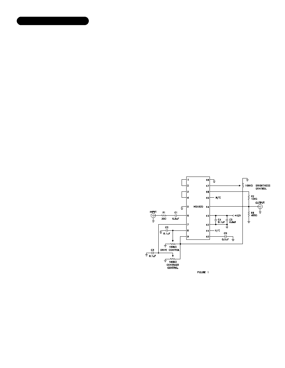
Pin 6 is the video input pin. The video input signal is coupled
to this point through a 30
, 10µF 'RC' filter as shown in figure
two. The MSK 620 is designed to receive input voltages as high
as ±13.5V.
VIDEO INPUT
Pin 16 is the (-) clamp input pin. This pin is the inverting input
to the clamp comparator. A 10K
feedback resistor is con-
nected from this pin to the output pin of the amplifier (pin 14).
When the clamp comparator is enabled, the voltage at pin 16 is
compared to the voltage at pin 17, which is the non-inverting
input of the clamp comparator. A source or sink current is gen-
erated at pin 10 to charge or discharge the clamp cap and sup-
ply DC bias to the video amplifier. The DC voltage at pin 17 is
user adjustable through a 100K
potentiometer voltage divider
to Vref (see figure 2). In DC coupled cathode drive applications,
brightness can be varied by varying the DC voltage at pin 17.
CLAMP CONNECTIONS
Pin 11 is the clamp gate input pin and is driven by a TTL back
porch clamp signal. A voltage level of +1.3V or less is a "low
level" and a voltage level of +1.5V or greater is a "high level".
An active low level at this pin enables the clamp comparator
section so that DC restoration can be accomplished. This pin
should be held at a "high" logic level when a back porch clamp
signal is not used.
DC RESTORATION
Pins 15 is a no connect pin and should be tied to the nearest
available video ground plane.
NO CONNECT PINS
A typical single video channel connection diagram for the
MSK 620 is shown in figure one above. The DC voltage at pin
6 is internally fixed at +2.6V and the video signal is AC coupled
to the input. An internal reference voltage generator supplies a
+5.0VDC level at pin 9 for use with the contrast, drive and
brightness control potentiometers. With pin 8 at 0V, minimum
gain is realized. With pin 8 at 4V, maximum gain is realized.
The clamp gate input at pin 11 accepts a TTL level clamp signal
for DC restoration during the back porch segment of the video
signal. Pin 17 is the brightness control input pin and accepts a
zero to four volt DC level. This level sets the black level of the
signal. If pin 17=+1VDC the signal black level will be +1VDC.
The 499
load resistor biases the class A output stage and
should be included during the power dissipation calculation stage.
499
is the minimum recommended value of load resistance for
the MSK 620.
Pin 10 is the clamp comparator output pin. A capacitance of
approximately 0.1µF is connected from this pin to ground. Dur-
ing the "back porch" portion of the clamp signal, the clamp ca-
pacitor is either charged or discharged to match the voltage set
on the non-inverting input of the clamp comparator (pin 16).
During the video portion of the input signal, the clamp compara-
tor is disabled and the clamp cap holds the proper DC bias in the
video amplifier.
CLAMP CAP
OUTPUT
Pin 14 is the video output pin. Since the output of the MSK
620 is a push pull design, there is no need for an external pullup
resistor. A 499
load resistor to analog ground will optimize
the output stage current level and bandwidth and is highly rec-
ommended.
POWER SUPPLY CONNECTIONS
Pin 13 is the positive power supply pin. Convenient internal
power supply decoupling consists of a parallel combination of
three capacitors ranging from 0.01µF to 0.47µF. The user is
advised to connect at least a 4.7µF tantalum decoupling capaci-
tor as close to the power supply pin as possible.
Vref OUTPUT
Pin 9 is the Vref output pin. This pin connects to the output of
an ultra stable 5.0VDC reference voltage generator internal to
the MSK 620. This reference is used as a voltage source for the
contrast, drive and clamp inputs.
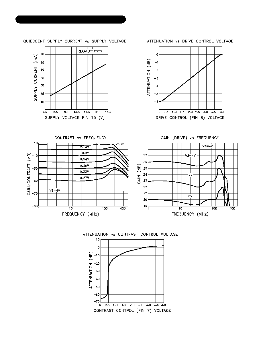
Pin 8 is the drive control input. This pin accepts a DC voltage
to control overall gain. Pin 8 is internally decoupled to ground
with a 0.1uF capacitor. With 0V at pin 8, the gain is minimum
(-6dB). With 4V at pin 8, the gain is maximum (0dB). Drive
control is approximated by the following formula:
ATTENUATION (dB) = (1.5) x (DRIVE VOLTAGE) - (6dB)
See graph of Attenuation vs. Drive Control Voltage.
DRIVE CONTROL
CONTRAST CONTROL
To achieve contrast control, pin 1 is shorted to pin 2 and pin 3
is shorted to pin 4. The voltages at pins 1 and 4 are controlled
by the input voltage at pin seven. As the voltage at pin 7 in-
creases, the voltages at pins 1 and 4 become offset. With pin 7
at zero volts, pins 1 and 4 are at minimum offset and the con-
trast is set to the minimum value of -38dB typical. With pin 7 at
4V, pins 1 and 4 are at maximum offset and contrast is maxi-
mized to +26dB. Pin 7 is internally decoupled to ground with a
0.1uF capacitor.
Rev. B 9/02
3
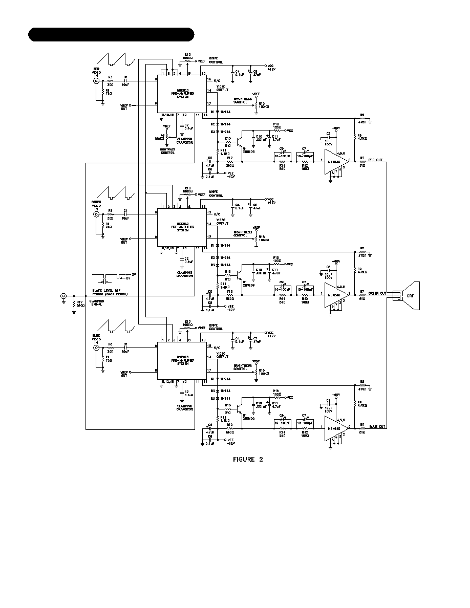
COMPLETE RGB VIDEO SYSTEM
A typical connection diagram for a red, green, blue video amplifier system is shown in Figure 2. To achieve optimum contrast
tracking, a master slave contrast connection is utilized. This is accomplished by connecting pins 1 and 2 of all three preamplifiers
together and using the contrast control of one channel to vary the contrast of all three channels simultaneously. White balance is
achieved through individual drive controls. Black level can also be adjusted for each channel by adjusting the voltage at pin 17. If the
cathode is AC coupled, the video signal is DC restored at the cathode. In that case black level clamping can be accomplished by
biasing pin 17 to the desired black level. The video output pins of the MSK 620 rests at approximately +3.9VDC and the input of
the MSK 640 must be biased at approximately +1.55VDC. D1, D2, D3 and Q1 act as a level shifting stage to match the DC level
requirements of the preamplifier and the driver. Black level control is accomplished with R8 and R9 sampling the output and feeding
it back to the clamping section of the MSK 620. This scheme provides black level control superior to locally sampling the MSK 620
output and feeding that back to the clamping section.
Rev. B 9/02
5