8170 Thompson Road Cicero, N.Y. 13039
M.S.KENNEDY CORP.
(315) 699-9201
FEATURES:
Ultra Fast Rise Time - 2.8nS Typical
Wide Bandwidth - 200 MHz Typical
Variable Gain - 0 to 100 V/V
On Board Reference Output
50 Vpp Output Voltage Swing
Blanking Capability
User Adjustable Brightness and Contrast
25,000 V/µSec Slew Rate
Replaces TP1900 And Max 445
HIGH PERFORMANCE,
HIGH VOLTAGE
VIDEO DISPLAY DRIVER
1900
High Resolution Mono-Chrome Displays
High Resolution RGB Displays
High Speed, High Voltage Amplification for ATE
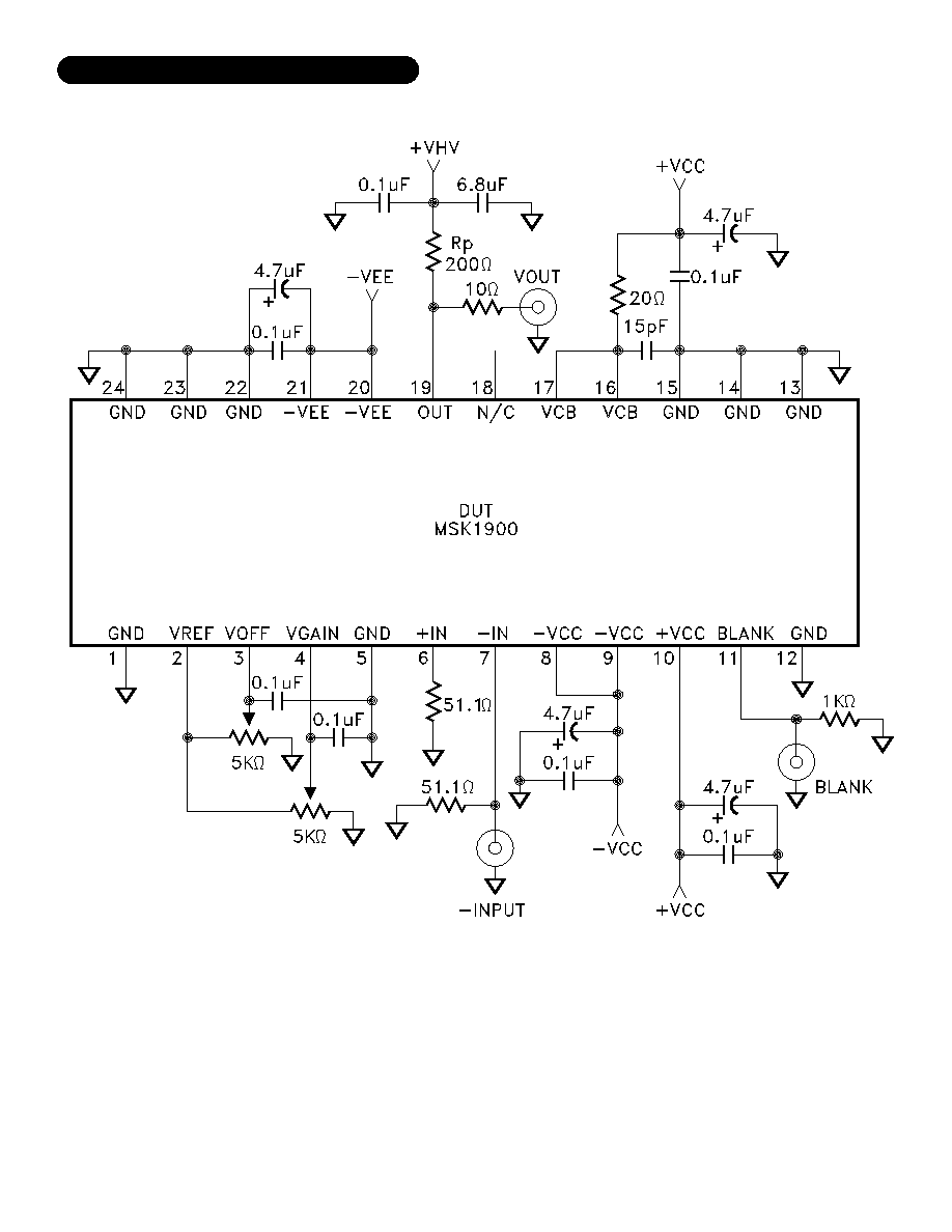
TYPICAL APPLICATIONS
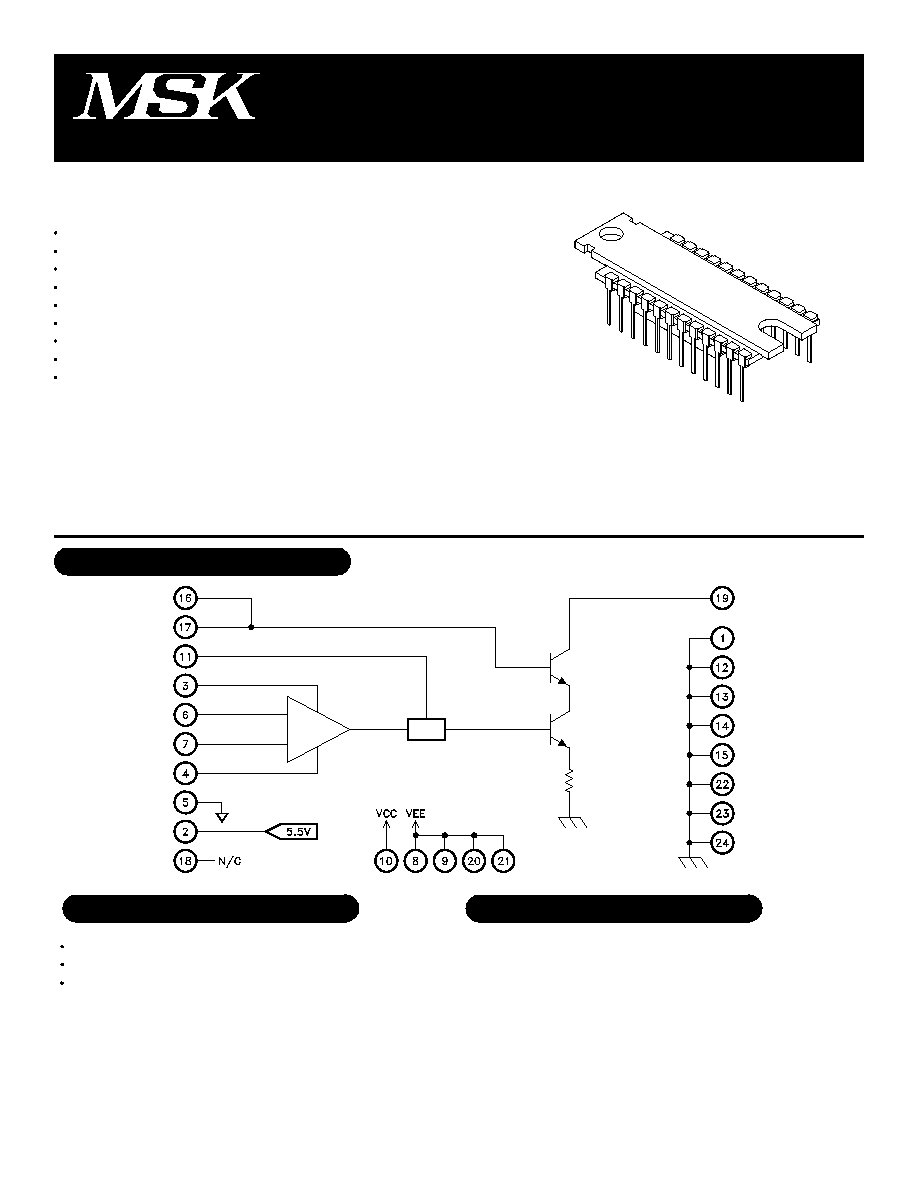
PIN-OUT INFORMATION
1
2
3
4
5
6
7
8
Ground
V
REF
V
OFF
V
GAIN
Ground
+Input
-Input
V
EE
9
10
11
12
13
14
15
16
V
EE
V
CC
Blank
Ground
Ground
Ground
Ground
V
CB
DESCRIPTION:
The MSK 1900 is a high performance, high voltage, variable gain video amplifier capable of directly driving high resolu-
tion video displays. The MSK 1900 features differential inputs and a linearly adjustable gain stage with an output offset
adjustment which allows it to be a versatile performer well suited for many applications. A TTL level blanking input is
available to set the output to a predetermined black level independent of signal input. The MSK 1900 is packaged in a cost
effective, 24 pin power dip which can be bolted directly to a heat sink for efficient thermal management.
EQUIVALENT SCHEMATIC
ISO-9001 CERTIFIED BY DSCC
1
Rev. B 9/99
17
18
19
20
21
22
23
24
V
CB
N/C
Output
V
EE
V
EE
Ground
Ground
Ground
NOTE: All pins must be connected for proper operation if
labeled.

The V
GAIN
control (contrast) input is designed to allow the
user to vary the video gain. By simply applying a DC voltage
from 0V to V
REF
, the video gain can be linearly adjusted from 0
to 100V/V. The V
GAIN
input should be connected to the V
REF
pin through a 5k
pot to ground. For convenient stable gain
adjustment, a 0.1µF bypass capacitor should be connected near
the V
GAIN
input pin to prevent output instability due to noisy
sources. Digital gain control can be accomplished by connect-
ing a D/A converter to the V
GAIN
pin. However, some tempera-
ture tracking performance may be lost when using an external
DC voltage source other than V
REF
for gain adjustment.
The overall video output of the MSK 1900 can be charac-
terized using the following expression:
Vpp=V
HV
-V
OUT
V
HV
-V
OUT
=(V
IN
)(V
GAIN
)(Rp)(0.08)
Here is a sample calculation for the MSK1900:
Given information
V
IN
=0.7V
V
GAIN
=1VDC
Rp=200
(external)
V
HV
=70VDC
V
HV
-V
OUT
=(0.7V)(1V)(.08)(200
)
V
HV
-V
OUT
=11.2Vpp Nominal
The expected video output would swing from approximately
+70V to +58.8V assuming that V
OFF
=0V. This calculation
should be used as a nominal result because the overall gain may
vary as much as ±10% due to internal high speed device varia-
tions. Changing ambient conditions can also effect the video
gain of the amplifier slightly. It is wise to connect all video
amplifiers to a common heat sink to maximize thermal tracking
when multiple amplifiers are used in applications such as RGB
systems. Additionally, only one of the V
REF
outputs should be
shared by all three amplifiers. This voltage should be buffered
with a suitable low-drift op-amp for best tracking performance.
APPLICATION NOTES
POWER SUPPLIES
The input stage of the MSK 1900 requires power supplies of
+10V and -10.5V for optimum operation. The negative power
supply can be increased to -12V if -10.5V is not available, but
additional power dissipation will cause the internal temperature
to rise. Both low voltage power supplies sould be effectively
decoupled with tantalum capacitors (at least 1µF) connected as
close to the amplifiers pins as possible. The MSK 1900 has
internal 0.01µF capacitors that also improve high frequency per-
formance. Additionally, it is also recommended to put 0.1µF
decoupling capacitors on the +10V and -10.5V supplies as
well.
The high voltage power supply (+V
HV
) is connected to the
amplifiers output stage and must be kept as stable as possible.
The internal Rp is connected to +V
HV
and as such, the amplifi-
ers DC output is directly related to the high voltage value. The
+V
HV
pin of the hybrid should be decoupled to ground with as
large a capacitor as possible to improve output stability.
V
GAIN
CONTROL INPUT
VIDEO INPUTS
The analog inputs (±V
IN
) are designed to accept RS343
signals, ±0.714V
PP
, and operate properly with a common mode
range of ±0.5V with respect to ground. Therefore, it is recom-
mended that the input signal be limited to ±1.3V with respect
to ground, (signal + common mode). Although large offsets of
±2V (with respect to ground, signal included) can be tolerated
without damage to the hybrid, output linearity suffers and there-
fore it is not recommended.
The output pin of the MSK 1900 can be protected from tran-
sients by connecting reversed biased ultra-low capacitance di-
odes from the output pin to both +V
HV
and ground. The output
can also be protected from arc voltages by inserting a small value
(50-100
) resistor in series with the amplifier. This resistor will
reduce system bandwidth along with the load capacitance, but a
series inductor can reduce the problem substantially.
OUTPUT PROTECTION
VIDEO OUTPUT
When power is first applied and V
IN
=V
GAIN
=V
OFF
=0V, the
output will be practically at the +V
HV
rail voltage. The output
voltage is a function of the value of Rp and also the V
GAIN
and
V
OFF
DC inputs. The bandwidth of the amplifier largely depends
on both Rp and Lp. With +V
HV
set to +70V and total
Rp=200
, the device is capable of approximately 62Vpp total
output swing.
The MSK 1900 is conservatively specified with low values
for external Lp which yield about 5% overshoot. Additional
peaking can be obtained by using a high self-resonant frequency
inductor in series with +V
HV
pin. Since this value of inductance
can be very dependent on circuit layout, it is best to determine
its value by experimentation. A good starting point is typically
0.47µH for the MSK 1900.
SUPPLY SEQUENCING
The power supply sequence is +V
HV
, V
CC
, V
EE
followed by
the other DC control inputs. If power supply sequencing is not
possible, the time difference between each supply should be
less than five milliseconds. If the DC control signals are being
generated from a low impedance source other than the V
REF
output, reverse biased diodes should be connected from each
input (V
GAIN
, V
OFF
) to the +V
CC
pin. This will protect the inputs
until +V
CC
is turned off.
3
Rev. B 9/99
V
CB
The V
CB
input is the base connection to the output stage con-
sisting of a common base, high voltage stage and a high speed,
low voltage current amplifier in a cascode arrangement. This
input requires a very stable 10V DC nominal voltage. Any AC
signals at this point will be amplified and reflected in the output.
The PSRR of the output stage is directly related to the stability
of this V
CB
voltage.

(T
C
= 25°C, V
HV
= 70V, R
P
= 200
)
APPLICATION NOTES CON'T
0
100
80
80
0
35
35
50
1.6
7.8
6.5
5.6
0
6.1
4.9
10
1.6
13.9
11.4
15.6
The video input can be electrically disconnected from the
amplifier by applying a TTL high input to the blank pin. When
this occurs, the output will be set to approximately +V
HV
. The
V
GAIN
and V
OFF
control pins have little or no effect on the output
when it is in blank mode.
When the TTL compatible blank input is not used, the pin
must be connected to ground to enable the amplifier. The blank
input will float high when left unconnected which will disable
the video.
BLANK INPUT
The MSK 1900 has an on board buffered DC zener reference
output. The V
REF
output is nominally 5.5V DC and has full
temperature test limits of 5.2V to 5.8V DC. This output is
provided for gain and offset adjustment and can source up to
4mA of current.
V
REF
OUTPUT
TOTAL
P
D
Watts
V
O
- V
BLACK
IC P
D
Watts
P
LOAD
Watts
The MSK 1900 package is electrically isolated from the inter-
nal circuitry, allowing direct connection to a heat sink.
The power dissipation of the amplifier depends mainly on
the load requirements, bandwidth, pixel size, black level and the
value of the external Rp. Refer to the following table for typical
power levels for selected video conditions:
THERMAL MANAGEMENT
4
Rev. B 9/99
The voltage developed across the external load resistor with a
0V video input to the MSK 1900 is the black level. This voltage
may be changed by adjusting the load resistor or by varying the
output quiescent current of the MSK 1900 as described in V
OFF
above. The black level could also be effected by the V
GAIN
con-
trol voltage if the video input has a DC component. AC coupling
of the video input will prevent this phenomenon from occurring.
BLACK LEVEL
V
OFF
is the output offset (brightness) control used to set the
output quiescent current and consequently the DC output volt-
age (black level). Output quiescent current adjustment range is
from several µA to 100mA nominal (80 to 130 mA actual).
Normally a 5K potentiometer is connected between V
REF
and
GND to this input, but any 0 - 5.5V external DC source may be
used. A 0.1µF capacitor should be connected from this pin to
signal ground to improve the amplifier's stability.
V
OFF
POWER DISSIPATION TABLE
Duty
Cycle %