1
TP3061
MOTOROLA RF DEVICE DATA
The RF Line
UHF Power Transistor
The TP3061 is designed for 960 MHz mobile base stations in both analog and
digital applications. It incorporates high value emitter ballast resistors, gold
metallizations and offers a high degree of reliability and ruggedness. Including
double input and output matching networks, the TP3060 features high
impedances and is easy to match.
Ě
Motorola Advanced Amplifier Concept Package
Ě
Oxynitride Passivation
Ě
Specified 26 Volts, 960 MHz Characteristics
Output Power = 45 Watts
Minimum Gain = 8.0 dB
Efficiency = 50%
Ě
Circuit board photomaster available upon request by contacting
RF Tactical Marketing in Phoenix, AZ.
MAXIMUM RATINGS
Rating
Symbol
Value
Unit
CollectorşEmitter Voltage
VCER
40
Vdc
CollectorşBase Voltage
VCBO
48
Vdc
EmitterşBase Voltage
VEBO
4.0
Vdc
Collector Current -- Continuous
IC
10
Adc
Total Device Dissipation @ TC = 25
░
C
Derate above 25
░
C
PD
175
1.0
Watts
W/
░
C
Storage Temperature Range
Tstg
ş 65 to +150
░
C
Operating Junction Temperature
TJ
200
░
C
THERMAL CHARACTERISTICS
Characteristic
Symbol
Max
Unit
Thermal Resistance, Junction to Case (1) at 70
░
C Case
R
JC
1.2
░
C/W
ELECTRICAL CHARACTERISTICS
(TC = 25
░
C unless otherwise noted.)
Characteristic
Symbol
Min
Typ
Max
Unit
OFF CHARACTERISTICS
CollectorşEmitter Breakdown Voltage
(IC = 60 mA, RBE = 75
)
V(BR)CER
40
--
--
Vdc
EmitterşBase Breakdown Voltage
(IC = 6.0 mAdc)
V(BR)EBO
3.5
--
--
Vdc
CollectorşBase Breakdown Voltage (IE = 60 mAdc)
V(BR)CBO
48
--
--
Vdc
CollectorşEmitter Leakage (VCE = 26 V, RBE = 75
)
ICER
--
--
15
mA
NOTE:
(continued)
1. Thermal resistance is determined under specified RF operating condition.
Order this document
by TP3061/D
MOTOROLA
SEMICONDUCTOR TECHNICAL DATA
TP3061
45 W, 960 MHz
UHF POWER
TRANSISTOR
NPN SILICON
CASE 333Aş02, STYLE 2
ę
Motorola, Inc. 1994
REV 6
TP3061
2
MOTOROLA RF DEVICE DATA
ELECTRICAL CHARACTERISTICS -- continued
(TC = 25
░
C unless otherwise noted.)
Characteristic
Symbol
Min
Typ
Max
Unit
ON CHARACTERISTICS
DC Current Gain
(IC = 1.0 Adc, VCE = 10 Vdc)
hFE
15
--
100
--
DYNAMIC CHARACTERISTICS
Output Capacitance (2)
(VCB = 26 V, IE = 0, f = 1.0 MHz)
Cob
45
60
--
pF
FUNCTIONAL TESTS
CommonşEmitter Amplifier Power Gain
(VCC = 26 V, Pout = 45 W, ICQ = 200 mA, f = 960 MHz)
Gp
8.0
8.8
--
dB
Collector Efficiency
(VCC = 26 V, Pout = 45 W, f = 960 MHz)
50
53
--
%
Load Mismatch
(VCC = 26 V, Pout = 45 W, ICQ = 200 mA,
Load VSWR = 5:1, at all phase angles)
No Degradation in Output Power
Before and After Test
Overdrive
(VCC = 26 V, Pin = 15 W, f = 960 MHz)
OD
No Degradation in Output Power
NOTE:
2. Value of "Cob" is that of die only. It is not measurable in TP3061 because of internal matching network.
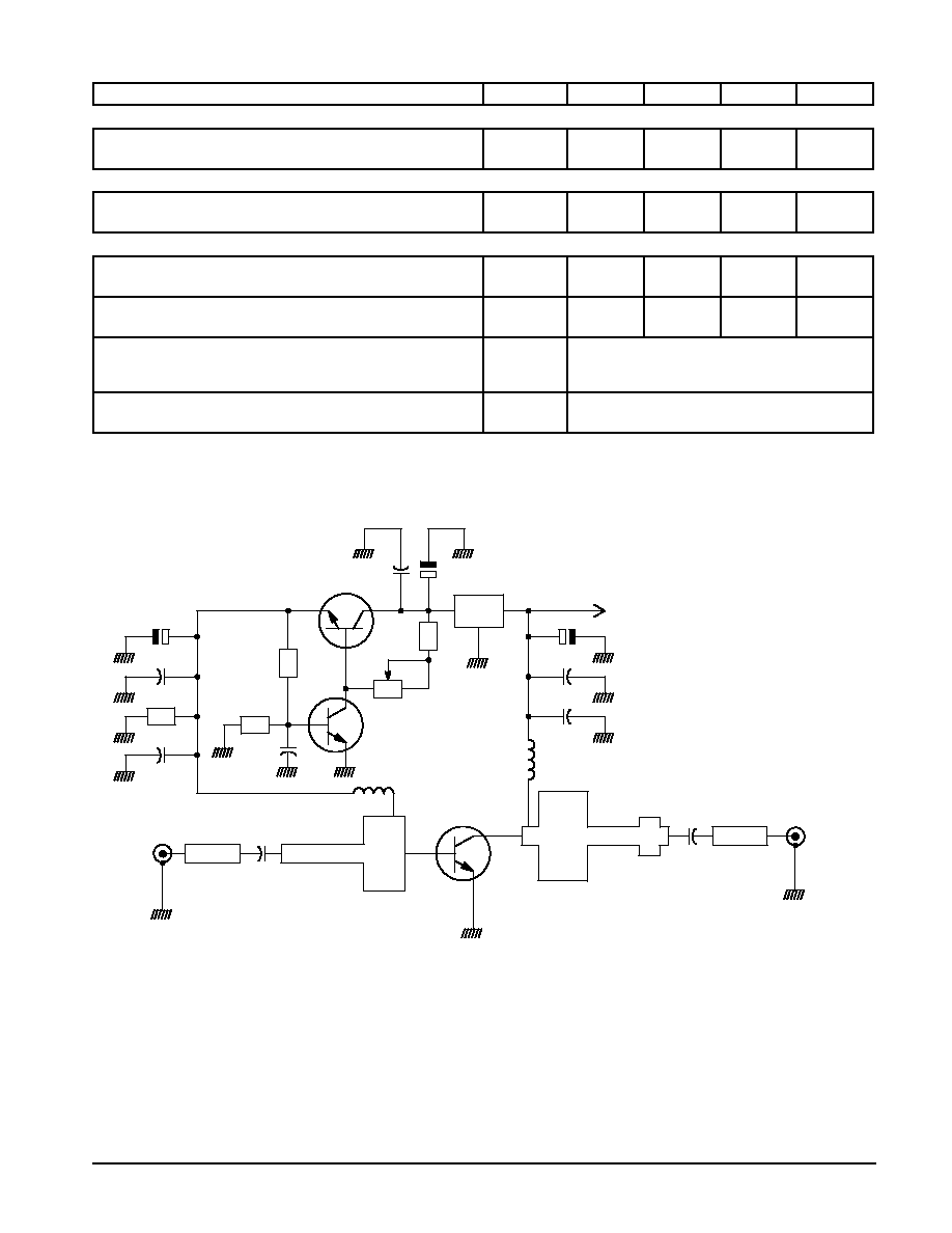
Figure 1. 960 MHz Test Circuit
C1, C4, C7, C12 -- Capacitor Chip 0805 330 pF 5%
C2 -- Capacitor Chip 82 pF ATC
C5, C11, C8 -- Capacitor Chip 0805 15 nF 5%
C6, C9, C10 -- Capacitor Chip 0805 6.0, 8.0
Á
F 35 V
L1, L2 -- 1.5 Turns #18 AWG Choke
R1 -- Chip Resistor 47
1206 5%
R2 -- Chip Resistor 270
0805 5%
R3 -- Chip Resistor 47
0805 5%
R4 -- Chip Resistor 100
0805 5%
R5 -- Trimmer 1.0 k
T1 -- SMD Transistor MJD31C or Similar
T2 -- SMD Transistor
T3 -- Voltage Regulator 7805
Board Material -- 1/50
, Teflon Glass,
r = 2.5,
Cu Clad 2 Sides, 35
Á
m Thick
RF INPUT
50
RF OUTPUT
50
D.U.T.
+ VCC
+
+
R3
C10
C11
C12
C6
C5
R1
C4
R2
C7
T1
C1
L2
L1
R5
C6
T3
C8
C9
R4
C2
T2
+
3
TP3061
MOTOROLA RF DEVICE DATA
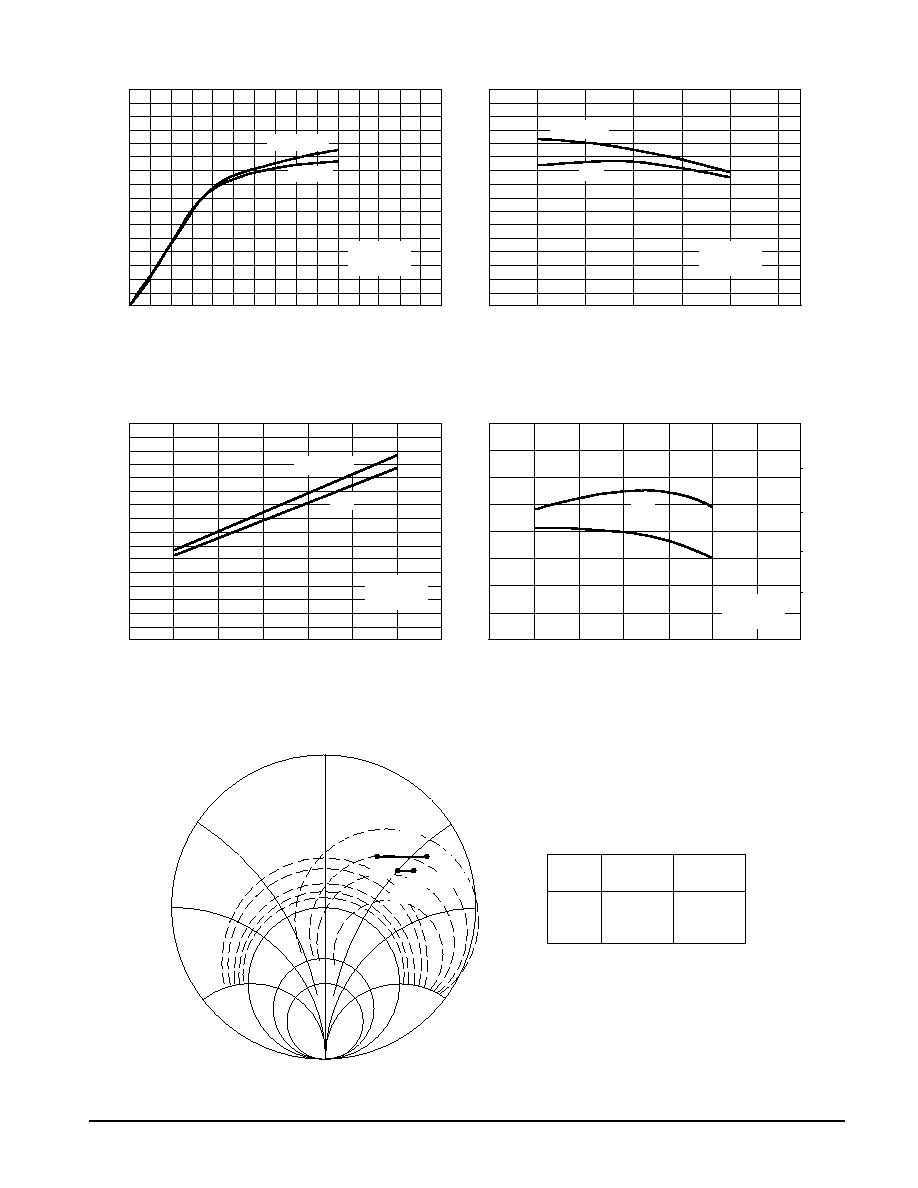
Figure 2. Output Power versus Input Power
Figure 3. Output Power versus Frequency
Figure 4. Power Output versus Supply Voltage
Figure 5. Typical Broadband Circuit Performance
Figure 6. Series Equivalent Input/Output Impedances
ZOL* = Conjugate of the optimum load
ZOL* =
impedance. Into which the device
ZOL* =
operates at a given output power,
ZOL* =
voltage, and frequency.
Pout = 45 W VCE = 26 V
f
MHz
ZIN
OHMS
ZOL*
OHMS
850
900
950
--
2.8 + j6
3.95 + j3.55
--
4.1 + j5
3.7 + j5.2
TYPICAL CHARACTERISTICS
P
o
, OUTPUT
POWER (W
A
TTS)
80
70
60
50
40
30
20
10
0
2
4
6
8
10
12
14
Pin, INPUT POWER (WATTS)
f = 935 MHz
VCC = 26 V
IQ = 200 mA
960 MHz
P
o
, OUTPUT
POWER (W
A
TTS)
80
70
60
50
40
30
20
10
0
880
f, FREQUENCY (MHz)
900
920
940
960
980
1000
VCC = 26 V
IQ = 200 mA
Pin = 10 W
7 W
P
o
, OUTPUT
POWER (W
A
TTS)
80
70
60
50
40
30
20
10
0
18
VCC, SUPPLY VOLTAGE (VOLTS)
20
22
24
26
28
30
32
f = 960 MHz
IQ = 200 mA
Pin = 10 W
7 W
G
p
, POWER GAIN (dB)
c
, COLLECT
OR EFFICIENCY
(%)
70
60
12
10
f, FREQUENCY (MHz)
8
6
4
50
40
30
Gp
c
VCC = 26 V
IQ = 200 mA
880
900
920
940
960
980
1000
0
5
10
20
ş 20
ş 10
ş 5
2
3
10
20
30
1
f = 960 MHz
ZIN
ZOL*
f = 960 MHz
900
900
TP3061
4
MOTOROLA RF DEVICE DATA
┬
┬
┬
┬
┬
┬
┬┬
┬┬
┬┬
┬
┬
┬
┬┬
┬┬
┬┬
┬┬
┬┬
┬┬
┬┬
┬┬
┬┬
┬┬
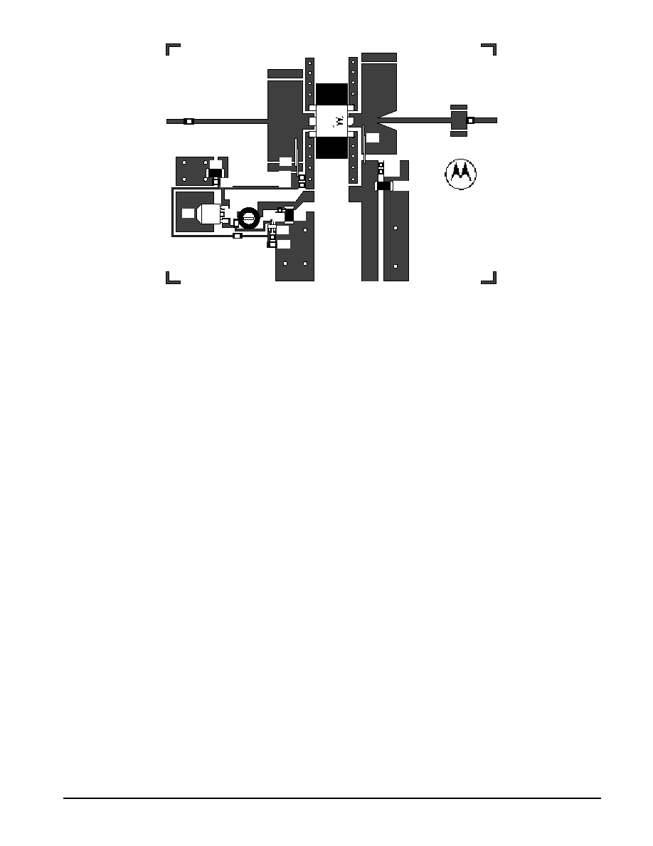
TP3061
MR8923
960 MHz
IN
OUT
C1
C6
R1
R5
T1
R4
R3
R2
C7
T2
C9
C8
C5
C4
TP3061
L2
L3
C12
C11
C10
C2
Figure 7. Test Circuit -- Component Locations

5
TP3061
MOTOROLA RF DEVICE DATA
PACKAGE DIMENSIONS
CASE 333Aş02
ISSUE C
DIM
A
MIN
MAX
MIN
MAX
MILLIMETERS
0.965
0.985
24.52
25.01
INCHES
B
0.390
0.410
9.91
10.41
C
0.250
0.290
6.35
7.36
D
0.075
0.090
1.91
2.28
E
0.095
0.115
2.42
2.92
F
0.110
0.130
2.80
3.30
H
0.155
0.175
3.94
4.44
J
0.004
0.006
0.11
0.15
K
0.090
0.116
2.29
2.94
L
0.725 BSC
18.41 BSC
N
0.415
0.435
10.55
11.04
Q
0.120
0.135
3.05
3.42
NOTES:
1. DIMENSIONING AND TOLERANCING PER ANSI
Y14.5M, 1982.
2. CONTROLLING DIMENSION: INCH.
STYLE 2:
PIN 1. EMITTER
2. BASE
3. EMITTER
4. EMITTER
5. COLLECTOR
6. EMITTER
IDENTIFICATION
NOTCH
N
L
E
J
H
C
SEATING
PLANE
1
2
3
4
5
6
K
2 PL
D
4 PL
F
2 PL
Q
2 PL
şBş
M
A
M
0.13 (0.005)
B
M
T
şAş
şTş

TP3061
6
MOTOROLA RF DEVICE DATA
Motorola reserves the right to make changes without further notice to any products herein. Motorola makes no warranty, representation or guarantee regarding
the suitability of its products for any particular purpose, nor does Motorola assume any liability arising out of the application or use of any product or circuit,
and specifically disclaims any and all liability, including without limitation consequential or incidental damages. "Typical" parameters can and do vary in different
applications. All operating parameters, including "Typicals" must be validated for each customer application by customer's technical experts. Motorola does
not convey any license under its patent rights nor the rights of others. Motorola products are not designed, intended, or authorized for use as components in
systems intended for surgical implant into the body, or other applications intended to support or sustain life, or for any other application in which the failure of
the Motorola product could create a situation where personal injury or death may occur. Should Buyer purchase or use Motorola products for any such
unintended or unauthorized application, Buyer shall indemnify and hold Motorola and its officers, employees, subsidiaries, affiliates, and distributors harmless
against all claims, costs, damages, and expenses, and reasonable attorney fees arising out of, directly or indirectly, any claim of personal injury or death
associated with such unintended or unauthorized use, even if such claim alleges that Motorola was negligent regarding the design or manufacture of the part.
Motorola and
are registered trademarks of Motorola, Inc. Motorola, Inc. is an Equal Opportunity/Affirmative Action Employer.
Literature Distribution Centers:
USA: Motorola Literature Distribution; P.O. Box 20912; Phoenix, Arizona 85036.
EUROPE: Motorola Ltd.; European Literature Centre; 88 Tanners Drive, Blakelands, Milton Keynes, MK14 5BP, England.
JAPAN: Nippon Motorola Ltd.; 4-32-1, Nishi-Gotanda, Shinagawa-ku, Tokyo 141, Japan.
ASIA PACIFIC: Motorola Semiconductors H.K. Ltd.; Silicon Harbour Center, No. 2 Dai King Street, Tai Po Industrial Estate, Tai Po, N.T., Hong Kong.
TP3061/D
*TP3061/D*