
1
Motorola Bipolar Power Transistor Device Data
High Voltage NPN Silicon
Power Transistors
. . . designed for line operated audio output amplifier, Switchmode power supply
drivers and other switching applications.
·
250 V to 400 V (Min) -- VCEO(sus)
·
1 A Rated Collector Current
·
Popular TO220 Plastic Package
ОООООООООООООООООООООООО
ОООООООООООООООООООООООО
ОООООООООООООООООООООООО
ОООООООООООООООООООООООО
MAXIMUM RATINGS
ОООООООООО
ОООООООООО
ОООООООООО
ОООООООООО
Rating
ОООО
ОООО
ОООО
ОООО
Symbol
ООО
ООО
ООО
ООО
TIP47
ООО
ООО
ООО
ООО
TIP48
ООО
ООО
ООО
ООО
TIP49
ОООО
ОООО
ОООО
ОООО
TIP50
ООО
ООО
ООО
ООО
Unit
ОООООООООО
ОООООООООО
ОООООООООО
ОООООООООО
CollectorEmitter Voltage
ОООО
ОООО
ОООО
ОООО
VCEO
ООО
ООО
ООО
ООО
250
ООО
ООО
ООО
ООО
300
ООО
ООО
ООО
ООО
350
ОООО
ОООО
ОООО
ОООО
400
ООО
ООО
ООО
ООО
Vdc
ОООООООООО
ОООООООООО
ОООООООООО
ОООООООООО
CollectorBase Voltage
ОООО
ОООО
ОООО
ОООО
VCB
ООО
ООО
ООО
ООО
350
ООО
ООО
ООО
ООО
400
ООО
ООО
ООО
ООО
450
ОООО
ОООО
ОООО
ОООО
500
ООО
ООО
ООО
ООО
Vdc
ОООООООООО
ОООООООООО
ОООООООООО
ОООООООООО
EmitterBase Voltage
ОООО
ОООО
ОООО
ОООО
VEB
ОООООООООО
ОООООООООО
ОООООООООО
ОООООООООО
5.0
ООО
ООО
ООО
ООО
Vdc
ОООООООООО
ОООООООООО
ОООООООООО
ОООООООООО
ОООООООООО
Collector Current -- Continuous
Peak
ОООО
ОООО
ОООО
ОООО
ОООО
IC
ОООООООООО
ОООООООООО
ОООООООООО
ОООООООООО
ОООООООООО
1.0
2.0
ООО
ООО
ООО
ООО
ООО
Adc
ОООООООООО
ОООООООООО
ОООООООООО
Base Current
ОООО
ОООО
ОООО
IB
ОООООООООО
ОООООООООО
ОООООООООО
0.6
ООО
ООО
ООО
Adc
ОООООООООО
ОООООООООО
ОООООООООО
ОООООООООО
ОООООООООО
ОООООООООО
Total Power Dissipation
@ TC = 25
_
C
Derate above 25
_
C
ОООО
ОООО
ОООО
ОООО
ОООО
ОООО
PD
ОООООООООО
ОООООООООО
ОООООООООО
ОООООООООО
ОООООООООО
ОООООООООО
40
0.32
ООО
ООО
ООО
ООО
ООО
ООО
Watts
W/
_
C
ОООООООООО
ОООООООООО
ОООООООООО
ОООООООООО
ОООООООООО
Total Power Dissipation
@ TA = 25
_
C
Derate above 25
_
C
ОООО
ОООО
ОООО
ОООО
ОООО
PD
ОООООООООО
ОООООООООО
ОООООООООО
ОООООООООО
ОООООООООО
2.0
0.016
ООО
ООО
ООО
ООО
ООО
Watts
W/
_
C
ОООООООООО
ОООООООООО
ОООООООООО
ОООООООООО
ОООООООООО
Unclamped Inducting Load
Energy (See Figure 8)
ОООО
ОООО
ОООО
ОООО
ОООО
E
ОООООООООО
ОООООООООО
ОООООООООО
ОООООООООО
ОООООООООО
20
ООО
ООО
ООО
ООО
ООО
mJ
ОООООООООО
ОООООООООО
ОООООООООО
ОООООООООО
Operating and Storage Junction
Temperature Range
ОООО
ОООО
ОООО
ОООО
TJ, Tstg
ОООООООООО
ОООООООООО
ОООООООООО
ОООООООООО
65 to + 150
ООО
ООО
ООО
ООО
_
C
ОООООООООООООООООООООООО
ОООООООООООООООООООООООО
ОООООООООООООООООООООООО
ОООООООООООООООООООООООО
THERMAL CHARACTERISTICS
ООООООООООООО
ООООООООООООО
ООООООООООООО
ООООООООООООО
Characteristic
ООООО
ООООО
ООООО
ООООО
Symbol
ОООООО
ОООООО
ОООООО
ОООООО
Max
ООО
ООО
ООО
ООО
Unit
ООООООООООООО
ООООООООООООО
ООООООООООООО
ООООООООООООО
Thermal Resistance, Junction to Case
ООООО
ООООО
ООООО
ООООО
R
JC
ОООООО
ОООООО
ОООООО
ОООООО
3.125
ООО
ООО
ООО
ООО
_
C/W
ООООООООООООО
ООООООООООООО
ООООООООООООО
ООООООООООООО
Thermal Resistance, Junction to Ambient
ООООО
ООООО
ООООО
ООООО
R
JA
ОООООО
ОООООО
ОООООО
ОООООО
62.5
ООО
ООО
ООО
ООО
_
C/W
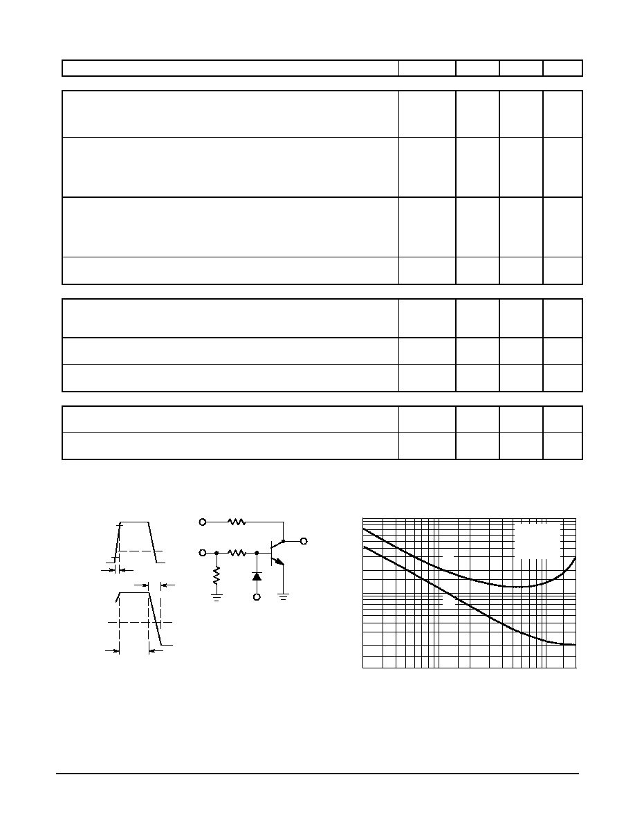
Figure 1. Power Derating
TC, CASE TEMPERATURE (
°
C)
0
100
0
10
160
20
30
60
80
40
140
40
20
120
P
D
, POWER DISSIP
A
TION (W
A
TTS)
TC
TC
0
1
2
3
4
TA
TA
Preferred devices are Motorola recommended choices for future use and best overall value.
MOTOROLA
SEMICONDUCTOR TECHNICAL DATA
Order this document
by TIP47/D
©
Motorola, Inc. 1995
TIP47
TIP49
TIP48
TIP50
1.0 AMPERE
POWER TRANSISTORS
NPN SILICON
250 300 350 400 VOLTS
40 WATTS
*Motorola Preferred Device
*
*
*
*
CASE 221A06
TO220AB
REV 1
TIP47 TIP49 TIP48 TIP50
2
Motorola Bipolar Power Transistor Device Data
ОООООООООООООООООООООООООООООООООО
ОООООООООООООООООООООООООООООООООО
ОООООООООООООООООООООООООООООООООО
ОООООООООООООООООООООООООООООООООО
ELECTRICAL CHARACTERISTICS
(TC = 25
_
C unless otherwise noted)
ООООООООООООООООООООООО
ООООООООООООООООООООООО
ООООООООООООООООООООООО
ООООООООООООООООООООООО
Characteristic
ОООО
ОООО
ОООО
ОООО
Symbol
ОООО
ОООО
ОООО
ОООО
Min
ОООО
ОООО
ОООО
ОООО
Max
ООО
ООО
ООО
ООО
Unit
ОООООООООООООООООООООООООООООООООО
ОООООООООООООООООООООООООООООООООО
ОООООООООООООООООООООООООООООООООО
ОООООООООООООООООООООООООООООООООО
OFF CHARACTERISTICS
ООООООООООООООООООООООО
ООООООООООООООООООООООО
ООООООООООООООООООООООО
ООООООООООООООООООООООО
ООООООООООООООООООООООО
ООООООООООООООООООООООО
CollectorEmitter Sustaining Voltage (1)
TIP47
(IC = 30 mAdc, IB = 0)
TIP48
TIP49
TIP50
ОООО
ОООО
ОООО
ОООО
ОООО
ОООО
VCEO(sus)
ОООО
ОООО
ОООО
ОООО
ОООО
ОООО
250
300
350
400
ОООО
ОООО
ОООО
ОООО
ОООО
ОООО
--
--
--
--
ООО
ООО
ООО
ООО
ООО
ООО
Vdc
ООООООООООООООООООООООО
ООООООООООООООООООООООО
ООООООООООООООООООООООО
ООООООООООООООООООООООО
ООООООООООООООООООООООО
ООООООООООООООООООООООО
ООООООООООООООООООООООО
Collector Cutoff Current
(VCE = 150 Vdc, IB = 0)
TIP47
(VCE = 200 Vdc, IB = 0)
TIP48
(VCE = 250 Vdc, IB = 0)
TIP49
(VCE = 300 Vdc, IB = 0)
TIP50
ОООО
ОООО
ОООО
ОООО
ОООО
ОООО
ОООО
ICEO
ОООО
ОООО
ОООО
ОООО
ОООО
ОООО
ОООО
--
--
--
--
ОООО
ОООО
ОООО
ОООО
ОООО
ОООО
ОООО
1.0
1.0
1.0
1.0
ООО
ООО
ООО
ООО
ООО
ООО
ООО
mAdc
ООООООООООООООООООООООО
ООООООООООООООООООООООО
ООООООООООООООООООООООО
ООООООООООООООООООООООО
ООООООООООООООООООООООО
ООООООООООООООООООООООО
ООООООООООООООООООООООО
Collector Cutoff Current
(VCE = 350 Vdc, VBE = 0)
TIP47
(VCE = 400 Vdc, VBE = 0)
TIP48
(VCE = 450 Vdc, VBE = 0)
TIP49
(VCE = 500 Vdc, VBE = 0)
TIP50
ОООО
ОООО
ОООО
ОООО
ОООО
ОООО
ОООО
ICES
ОООО
ОООО
ОООО
ОООО
ОООО
ОООО
ОООО
--
--
--
--
ОООО
ОООО
ОООО
ОООО
ОООО
ОООО
ОООО
1.0
1.0
1.0
1.0
ООО
ООО
ООО
ООО
ООО
ООО
ООО
mAdc
ООООООООООООООООООООООО
ООООООООООООООООООООООО
ООООООООООООООООООООООО
ООООООООООООООООООООООО
Emitter Cutoff Current
(VBE = 5.0 Vdc, IC = 0)
ОООО
ОООО
ОООО
ОООО
IEBO
ОООО
ОООО
ОООО
ОООО
--
ОООО
ОООО
ОООО
ОООО
1.0
ООО
ООО
ООО
ООО
mAdc
ОООООООООООООООООООООООООООООООООО
ОООООООООООООООООООООООООООООООООО
ОООООООООООООООООООООООООООООООООО
ОООООООООООООООООООООООООООООООООО
ON CHARACTERISTICS (1)
ООООООООООООООООООООООО
ООООООООООООООООООООООО
ООООООООООООООООООООООО
ООООООООООООООООООООООО
ООООООООООООООООООООООО
ООООООООООООООООООООООО
DC Current Gain
(IC = 0.3 Adc, VCE = 10 Vdc)
(IC = 1.0 Adc, VCE = 10 Vdc)
ОООО
ОООО
ОООО
ОООО
ОООО
ОООО
hFE
ОООО
ОООО
ОООО
ОООО
ОООО
ОООО
30
10
ОООО
ОООО
ОООО
ОООО
ОООО
ОООО
150
--
ООО
ООО
ООО
ООО
ООО
ООО
--
ООООООООООООООООООООООО
ООООООООООООООООООООООО
ООООООООООООООООООООООО
ООООООООООООООООООООООО
CollectorEmitter Saturation Voltage
(IC = 1.0 Adc, IB = 0.2 Adc)
ОООО
ОООО
ОООО
ОООО
VCE(sat)
ОООО
ОООО
ОООО
ОООО
--
ОООО
ОООО
ОООО
ОООО
1.0
ООО
ООО
ООО
ООО
Vdc
ООООООООООООООООООООООО
ООООООООООООООООООООООО
ООООООООООООООООООООООО
ООООООООООООООООООООООО
ООООООООООООООООООООООО
BaseEmitter On Voltage
(IC = 1.0 Adc, VCE = 10 Vdc)
ОООО
ОООО
ОООО
ОООО
ОООО
VBE(on)
ОООО
ОООО
ОООО
ОООО
ОООО
--
ОООО
ОООО
ОООО
ОООО
ОООО
1.5
ООО
ООО
ООО
ООО
ООО
Vdc
ОООООООООООООООООООООООООООООООООО
ОООООООООООООООООООООООООООООООООО
ОООООООООООООООООООООООООООООООООО
ОООООООООООООООООООООООООООООООООО
DYNAMIC CHARACTERISTICS
ООООООООООООООООООООООО
ООООООООООООООООООООООО
ООООООООООООООООООООООО
ООООООООООООООООООООООО
ООООООООООООООООООООООО
CurrentGain -- Bandwidth Product
(IC = 0.1 Adc, VCE = 10 Vdc, f = 2.0 MHz)
ОООО
ОООО
ОООО
ОООО
ОООО
fT
ОООО
ОООО
ОООО
ОООО
ОООО
10
ОООО
ОООО
ОООО
ОООО
ОООО
--
ООО
ООО
ООО
ООО
ООО
MHz
ООООООООООООООООООООООО
ООООООООООООООООООООООО
ООООООООООООООООООООООО
ООООООООООООООООООООООО
SmallSignal Current Gain
(IC = 0.2 Adc, VCE = 10 Vdc, f = 1.0 kHz)
ОООО
ОООО
ОООО
ОООО
hfe
ОООО
ОООО
ОООО
ОООО
25
ОООО
ОООО
ОООО
ОООО
--
ООО
ООО
ООО
ООО
--
(1) Pulse Test: Pulse width
v
300
µ
s, Duty Cycle
v
2.0%.
TURNON PULSE
APPROX
+11 V
Vin 0
VEB(off)
t1
APPROX
+11 V
Vin
t2
TURNOFF PULSE
t3
t1
7.0 ns
100 < t2 < 500
µ
s
t3 < 15 ns
DUTY CYCLE
2.0%
APPROX 9.0 V
RB and RC VARIED TO OBTAIN DESIRED CURRENT LEVELS.
SCOPE
RC
RB
VCC
Vin
Cjd << Ceb
4.0 V
Figure 2. Switching Time Equivalent Circuit
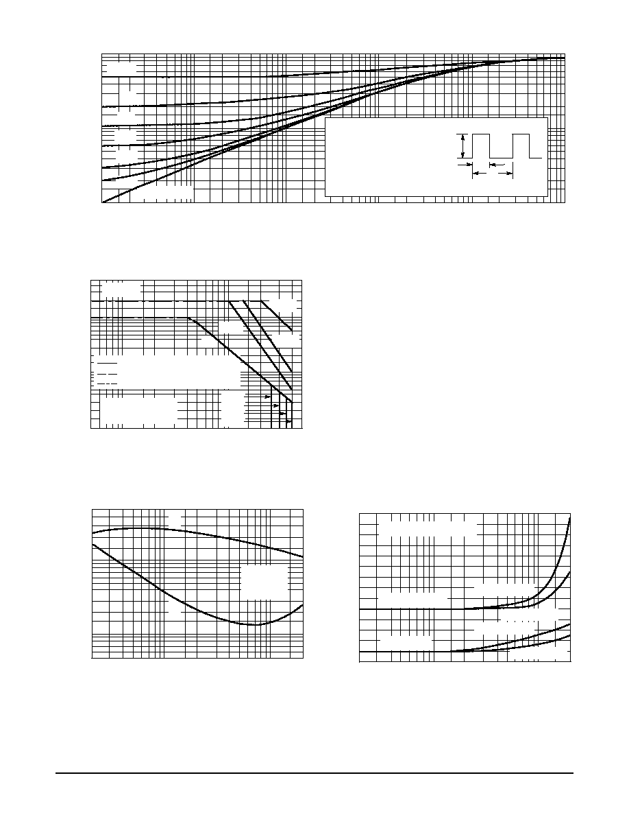
0.02
Figure 3. TurnOn Time
IC, COLLECTOR CURRENT (AMPS)
0.01
0.1
2.0
1.0
TJ = 25
°
C
VCC = 200 V
IC/IB = 5.0
t,
TIME (
s)
µ
0.5
0.2
0.1
0.05
0.05
0.5
0.02
1.0
tr
0.2
td
TIP47 TIP49 TIP48 TIP50
3
Motorola Bipolar Power Transistor Device Data
t, TIME (ms)
1.0
0.01
0.01
0.1
r(t)
,
TRANSIENT
THERMAL
RESIST
ANCE (NORMALIZED)
1.0
1.0
100
Z
JC(t) = r(t) R
JC
R
JC = 3.125
°
C/W MAX
D CURVES APPLY FOR POWER
PULSE TRAIN SHOWN
READ TIME AT t1
TJ(pk) TC = P(pk) Z
JC(t)
P(pk)
t1
t2
SINGLE PULSE
1.0 k
D = 0.5
0.2
0.05
DUTY CYCLE, D = t1/t2
Figure 4. Thermal Response
0.1
0.05
0.02
0.01
0.03
0.02
0.07
0.5
0.3
0.2
0.7
0.02
0.05
0.2
0.5
2.0
5.0
200
500
10
20
50
VCE, COLLECTOREMITTER VOLTAGE (VOLTS)
10
20
5.0
50
500
Figure 5. Active Region Safe Operating Area
0.02
0.05
SECONDARY BREAKDOWN LIMITED
THERMALLY LIMITED @ 25
°
C
BONDING WIRE LIMITED
1.0 ms
dc
100
µ
s
0.2
0.1
5.0
2.0
I C
, COLLECT
OR CURRENT
(AMPS)
CURVES APPLY
BELOW RATED VCEO
1.0
0.5
100
200
500
µ
s
TC
25
°
C
TIP47
TIP48
TIP49
TIP50
There are two limitations on the power handling ability of a
transistor: average junction temperature and second break-
down. Safe operating area curves indicate IC VCE limits of
the transistor that must be observed for reliable operation,
i.e., the transistor must not be subjected to greater dissipa-
tion than the curves indicate.
The data of Figure 5 is based on TJ(pk) = 150
_
C; TC is
variable depending on conditions. Second breakdown pulse
limits are valid for duty cycles to 10% provided TJ(pk)
v
150
_
C. TJ(pk) may be calculated from the data in
Figure 4. At high case temperatures, thermal limitations will
reduce the power that can be handled to values less than the
limitations imposed by second breakdown.
0.05
0.1
0.2
0.02
0.5
IC, COLLECTOR CURRENT (AMPS)
Figure 6. TurnOff Time
5.0
t,
TIME (
s)
µ
2.0
1.0
0.5
0.2
0.1
0.05
1.0
2.0
ts
TJ = 25
°
C
VCC = 200 V
IC/IB = 5.0
tf
IC, COLLECTOR CURRENT (AMPS)
+ 4.5
V
,
TEMPERA
TURE COEFFICIENTS (mV/
C)
°
+ 3.5
+ 2.5
+ 1.5
0
0.5
1.5
2.5
*APPLIES FOR IC/IB
hFE/5
VC FOR VCE(sat)
VB FOR VBE
Figure 7. Temperature Coefficients
0.02
0.05
0.1
0.2
0.5
1.0
2.0
+ 25
°
C to + 150
°
C
55
°
C to + 25
°
C
+ 25
°
C to + 150
°
C
55
°
C to + 25
°
C
+ 0.5
TIP47 TIP49 TIP48 TIP50
4
Motorola Bipolar Power Transistor Device Data
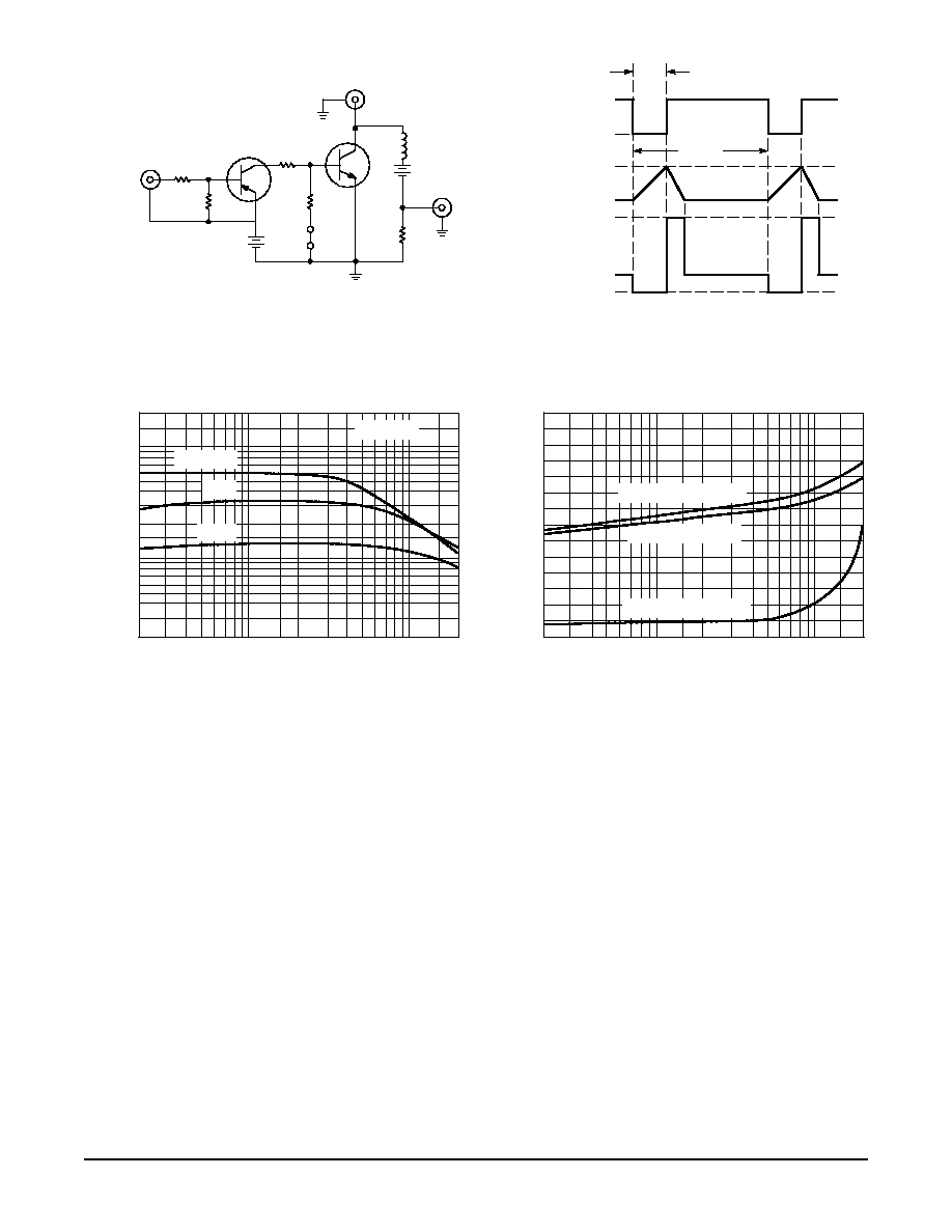
Figure 8. Inductive Load Switching
Note A: Input pulse width is increased until ICM = 0.63 A.
INPUT
50
MJE171
RBB1 =
150
100 mH
RBB2 =
100
VBB2 =
0
VBB1 = 10 V
VCE MONITOR
TUT
VCC = 20 V
IC MONITOR
RS =
0.1
50
0.63 A
0 V
5 V
tw
3 ms
(SEE NOTE A)
INPUT
VOLTAGE
COLLECTOR
CURRENT
COLLECTOR
VOLTAGE
VCER
0 V
10 V
100 ms
VCE(sat)
IC, COLLECTOR CURRENT (AMPS)
h
FE
, DC CURRENT
GAIN
Figure 9. DC Current Gain
100
200
0.04 0.06
0.2
2.0
0.02
60
40
20
10
6.0
4.0
0.1
Figure 10. "On" Voltages
VCE = 10 V
2.0
0.6
1.0
0.4
25
°
C
TJ = 150
°
C
55
°
C
1.4
0.02
IC, COLLECTOR CURRENT (AMPS)
1.0
0.8
0.4
1.2
0.6
0.2
0
0.04 0.06
0.1
0.2
0.4 0.6
V
, VOL
T
AGE (VOL
TS)
1.0
2.0
VBE(sat) @ IC/IB = 5.0 V
VBE(on) @ VCE = 4 V
VCE(sat) @ IC/IB = 5.0 V

TIP47 TIP49 TIP48 TIP50
5
Motorola Bipolar Power Transistor Device Data
PACKAGE DIMENSIONS
CASE 221A06
TO220AB
ISSUE Y
NOTES:
1. DIMENSIONING AND TOLERANCING PER ANSI
Y14.5M, 1982.
2. CONTROLLING DIMENSION: INCH.
3. DIMENSION Z DEFINES A ZONE WHERE ALL
BODY AND LEAD IRREGULARITIES ARE
ALLOWED.
STYLE 1:
PIN 1. BASE
2. COLLECTOR
3. EMITTER
4. COLLECTOR
DIM
MIN
MAX
MIN
MAX
MILLIMETERS
INCHES
A
0.570
0.620
14.48
15.75
B
0.380
0.405
9.66
10.28
C
0.160
0.190
4.07
4.82
D
0.025
0.035
0.64
0.88
F
0.142
0.147
3.61
3.73
G
0.095
0.105
2.42
2.66
H
0.110
0.155
2.80
3.93
J
0.018
0.025
0.46
0.64
K
0.500
0.562
12.70
14.27
L
0.045
0.060
1.15
1.52
N
0.190
0.210
4.83
5.33
Q
0.100
0.120
2.54
3.04
R
0.080
0.110
2.04
2.79
S
0.045
0.055
1.15
1.39
T
0.235
0.255
5.97
6.47
U
0.000
0.050
0.00
1.27
V
0.045
1.15
Z
0.080
2.04
B
Q
H
Z
L
V
G
N
A
K
F
1
2 3
4
D
SEATING
PLANE
T
C
S
T
U
R
J

TIP47 TIP49 TIP48 TIP50
6
Motorola Bipolar Power Transistor Device Data
How to reach us:
USA / EUROPE: Motorola Literature Distribution;
JAPAN: Nippon Motorola Ltd.; TatsumiSPDJLDC, Toshikatsu Otsuki,
P.O. Box 20912; Phoenix, Arizona 85036. 18004412447
6F SeibuButsuryuCenter, 3142 Tatsumi KotoKu, Tokyo 135, Japan. 0335218315
MFAX: RMFAX0@email.sps.mot.com TOUCHTONE (602) 2446609
HONG KONG: Motorola Semiconductors H.K. Ltd.; 8B Tai Ping Industrial Park,
INTERNET: http://DesignNET.com
51 Ting Kok Road, Tai Po, N.T., Hong Kong. 85226629298
Motorola reserves the right to make changes without further notice to any products herein. Motorola makes no warranty, representation or guarantee regarding
the suitability of its products for any particular purpose, nor does Motorola assume any liability arising out of the application or use of any product or circuit,
and specifically disclaims any and all liability, including without limitation consequential or incidental damages. "Typical" parameters can and do vary in different
applications. All operating parameters, including "Typicals" must be validated for each customer application by customer's technical experts. Motorola does
not convey any license under its patent rights nor the rights of others. Motorola products are not designed, intended, or authorized for use as components in
systems intended for surgical implant into the body, or other applications intended to support or sustain life, or for any other application in which the failure of
the Motorola product could create a situation where personal injury or death may occur. Should Buyer purchase or use Motorola products for any such
unintended or unauthorized application, Buyer shall indemnify and hold Motorola and its officers, employees, subsidiaries, affiliates, and distributors harmless
against all claims, costs, damages, and expenses, and reasonable attorney fees arising out of, directly or indirectly, any claim of personal injury or death
associated with such unintended or unauthorized use, even if such claim alleges that Motorola was negligent regarding the design or manufacture of the part.
Motorola and
are registered trademarks of Motorola, Inc. Motorola, Inc. is an Equal Opportunity/Affirmative Action Employer.
TIP47/D
*TIP47/D*