1
Motorola TMOS Power MOSFET Transistor Device Data
Designer's
TM
Data Sheet
TMOS V
Power Field Effect Transistor
DPAK for Surface Mount
NChannel EnhancementMode Silicon Gate
TMOS V is a new technology designed to achieve an onresis-
tance area product about onehalf that of standard MOSFETs. This
new technology more than doubles the present cell density of our
50 and 60 volt TMOS devices. Just as with our TMOS EFET
designs, TMOS V is designed to withstand high energy in the
avalanche and commutation modes. Designed for low voltage, high
speed switching applications in power supplies, converters and
power motor controls, these devices are particularly well suited for
bridge circuits where diode speed and commutating safe operating
areas are critical and offer additional safety margin against
unexpected voltage transients.
New Features of TMOS V
·
Onresistance Area Product about Onehalf that of Standard
MOSFETs with New Low Voltage, Low RDS(on) Technology
·
Faster Switching than EFET Predecessors
Features Common to TMOS V and TMOS EFETS
·
Avalanche Energy Specified
·
IDSS and VDS(on) Specified at Elevated Temperature
·
Static Parameters are the Same for both TMOS V and TMOS EFET
·
Surface Mount Package Available in 16 mm 13inch/2500 Unit Tape & Reel, Add T4 Suffix to Part Number
MAXIMUM RATINGS
(TC = 25
°
C unless otherwise noted)
Rating
Symbol
Value
Unit
DrainSource Voltage
VDSS
60
Vdc
DrainGate Voltage (RGS = 1.0 M
)
VDGR
60
Vdc
GateSource Voltage -- Continuous
GateSource Voltage
-- Single Pulse (tp
50 ms)
VGS
VGSM
±
20
±
25
Vdc
Vpk
Drain Current -- Continuous @ 25
°
C
Drain Current
-- Continuous @ 100
°
C
Drain Current
-- Single Pulse (tp
10
µ
s)
ID
ID
IDM
15
8.7
45
Adc
Apk
Total Power Dissipation @ 25
°
C
Derate above 25
°
C
Total Power Dissipation @ TA = 25
°
C, when mounted to minimum recommended pad size
PD
55
0.36
2.1
Watts
W/
°
C
Watts
Operating and Storage Temperature Range
TJ, Tstg
55 to 175
°
C
Single Pulse DraintoSource Avalanche Energy -- Starting TJ = 25
°
C
(VDD = 25 Vdc, VGS = 10 Vdc, IL = 15 Apk, L = 1.0 mH, RG = 25
)
EAS
113
mJ
Thermal Resistance -- Junction to Case
Thermal Resistance
-- Junction to Ambient
Thermal Resistance
-- Junction to Ambient, when mounted to minimum recommended pad size
R
JC
R
JA
R
JA
2.73
100
71.4
°
C/W
Maximum Lead Temperature for Soldering Purposes, 1/8
from case for 10 seconds
TL
260
°
C
Designer's Data for "Worst Case" Conditions -- The Designer's Data Sheet permits the design of most circuits entirely from the information presented. SOA Limit
curves -- representing boundaries on device characteristics -- are given to facilitate "worst case" design.
EFET, Designer's and TMOS V are trademarks of Motorola, Inc. TMOS is a registered trademark of Motorola, Inc.
Thermal Clad is a trademark of the Bergquist Company.
Preferred devices are Motorola recommended choices for future use and best overall value.
REV 2
Order this document
by MTD15N06V/D
MOTOROLA
SEMICONDUCTOR TECHNICAL DATA
TM
D
S
G
CASE 369A13, Style 2
DPAK Surface Mount
MTD15N06V
TMOS POWER FET
15 AMPERES
60 VOLTS
RDS(on) = 0.12 OHM
Motorola Preferred Device
©
Motorola, Inc. 1996

MTD15N06V
2
Motorola TMOS Power MOSFET Transistor Device Data
ELECTRICAL CHARACTERISTICS
(TJ = 25
°
C unless otherwise noted)
Characteristic
Symbol
Min
Typ
Max
Unit
OFF CHARACTERISTICS
DrainSource Breakdown Voltage
(VGS = 0 Vdc, ID = 250
µ
Adc)
Temperature Coefficient (Positive)
V(BR)DSS
60
--
--
67
--
--
Vdc
mV/
°
C
Zero Gate Voltage Drain Current
(VDS = 60 Vdc, VGS = 0 Vdc)
(VDS = 60 Vdc, VGS = 0 Vdc, TJ = 150
°
C)
IDSS
--
--
--
--
10
100
µ
Adc
GateBody Leakage Current (VGS =
±
20 Vdc, VDS = 0)
IGSS
--
--
100
nAdc
ON CHARACTERISTICS (1)
Gate Threshold Voltage
(VDS = VGS, ID = 250
µ
Adc)
Temperature Coefficient (Negative)
VGS(th)
2.0
--
2.7
5.0
4.0
--
Vdc
mV/
°
C
Static DrainSource OnResistance (VGS = 10 Vdc, ID = 7.5 Adc)
RDS(on)
--
0.08
0.12
Ohm
DrainSource OnVoltage (VGS = 10 Vdc)
(ID = 15 Adc)
(ID = 7.5 Adc, TJ = 150
°
C)
VDS(on)
--
--
2.0
--
2.2
1.9
Vdc
Forward Transconductance (VDS = 8.0 Vdc, ID = 7.5 Adc)
gFS
4.0
6.2
--
mhos
DYNAMIC CHARACTERISTICS
Input Capacitance
(VDS = 25 Vdc, VGS = 0 Vdc,
f = 1.0 MHz)
Ciss
--
469
660
pF
Output Capacitance
(VDS = 25 Vdc, VGS = 0 Vdc,
f = 1.0 MHz)
Coss
--
148
200
Reverse Transfer Capacitance
f = 1.0 MHz)
Crss
--
35
60
SWITCHING CHARACTERISTICS (2)
TurnOn Delay Time
(VDD = 30 Vdc, ID = 15 Adc,
VGS = 10 Vdc,
RG = 9.1
)
td(on)
--
7.6
20
ns
Rise Time
(VDD = 30 Vdc, ID = 15 Adc,
VGS = 10 Vdc,
RG = 9.1
)
tr
--
51
100
TurnOff Delay Time
VGS = 10 Vdc,
RG = 9.1
)
td(off)
--
18
40
Fall Time
G = 9.1
)
tf
--
33
70
Gate Charge
(See Figure 8)
(VDS = 48 Vdc, ID = 15 Adc,
VGS = 10 Vdc)
QT
--
14.4
20
nC
(See Figure 8)
(VDS = 48 Vdc, ID = 15 Adc,
VGS = 10 Vdc)
Q1
--
2.8
--
(VDS = 48 Vdc, ID = 15 Adc,
VGS = 10 Vdc)
Q2
--
6.4
--
Q3
--
6.1
--
SOURCEDRAIN DIODE CHARACTERISTICS
Forward OnVoltage (1)
(IS = 15 Adc, VGS = 0 Vdc)
(IS = 15 Adc, VGS = 0 Vdc, TJ = 150
°
C)
VSD
--
--
1.05
1.5
1.6
--
Vdc
Reverse Recovery Time
(See Figure 14)
(IS = 15 Adc, VGS = 0 Vdc,
dIS/dt = 100 A/
µ
s)
trr
--
59.3
--
ns
(See Figure 14)
(IS = 15 Adc, VGS = 0 Vdc,
dIS/dt = 100 A/
µ
s)
ta
--
46
--
(IS = 15 Adc, VGS = 0 Vdc,
dIS/dt = 100 A/
µ
s)
tb
--
13.3
--
Reverse Recovery Stored Charge
QRR
--
0.165
--
µ
C
INTERNAL PACKAGE INDUCTANCE
Internal Drain Inductance
(Measured from the drain lead 0.25
from package to center of die)
LD
--
4.5
--
nH
Internal Source Inductance
(Measured from the source lead 0.25
from package to source bond pad)
LS
--
7.5
--
nH
(1) Pulse Test: Pulse Width
300
µ
s, Duty Cycle
2%.
(2) Switching characteristics are independent of operating junction temperature.

MTD15N06V
3
Motorola TMOS Power MOSFET Transistor Device Data
TYPICAL ELECTRICAL CHARACTERISTICS
0
1
2
3
5
7
0
10
20
30
VDS, DRAINTOSOURCE VOLTAGE (VOLTS)
Figure 1. OnRegion Characteristics
I D
, DRAIN CURRENT
(AMPS)
2
4
6
8
10
0
5
10
20
30
I D
, DRAIN CURRENT
(AMPS)
VGS, GATETOSOURCE VOLTAGE (VOLTS)
Figure 2. Transfer Characteristics
0
5
10
15
20
30
0
0.05
0.10
0.20
R
DS(on)
, DRAINT
OSOURCE RESIST
ANCE (OHMS)
ID, DRAIN CURRENT (AMPS)
Figure 3. OnResistance versus Drain Current
and Temperature
Figure 4. OnResistance versus Drain Current
and Gate Voltage
0
10
20
40
50
60
10
100
Figure 5. OnResistance Variation with
Temperature
VDS, DRAINTOSOURCE VOLTAGE (VOLTS)
Figure 6. DrainToSource Leakage
Current versus Voltage
I DSS
, LEAKAGE (nA)
TJ = 25
°
C
VGS = 10 V
9 V
8 V
6 V
5 V
7 V
VGS = 10 V
TJ = 100
°
C
25
°
C
55
°
C
TJ = 55
°
C
25
°
C
100
°
C
VGS = 0 V
TJ = 125
°
C
5
15
25
4
6
15
25
25
30
VDS
10 V
0.15
R
DS(on)
, DRAINT
OSOURCE RESIST
ANCE (OHMS)
ID, DRAIN CURRENT (AMPS)
TJ = 25
°
C
0.13
0.11
0.09
0.07
0.05
10
5
0
15
20
25
30
VGS = 10 V
15 V
R
DS(on)
, DRAINT
OSOURCE RESIST
ANCE
(NORMALIZED)
TJ, JUNCTION TEMPERATURE (
°
C)
VGS = 10 V
ID = 7.5 A
2
1.6
1.2
0.8
0.4
50
25
0
25
50
75
100
125
150
175

MTD15N06V
4
Motorola TMOS Power MOSFET Transistor Device Data
POWER MOSFET SWITCHING
Switching behavior is most easily modeled and predicted
by recognizing that the power MOSFET is charge controlled.
The lengths of various switching intervals (
t) are deter-
mined by how fast the FET input capacitance can be charged
by current from the generator.
The published capacitance data is difficult to use for calculat-
ing rise and fall because draingate capacitance varies
greatly with applied voltage. Accordingly, gate charge data is
used. In most cases, a satisfactory estimate of average input
current (IG(AV)) can be made from a rudimentary analysis of
the drive circuit so that
t = Q/IG(AV)
During the rise and fall time interval when switching a resis-
tive load, VGS remains virtually constant at a level known as
the plateau voltage, VSGP. Therefore, rise and fall times may
be approximated by the following:
tr = Q2 x RG/(VGG VGSP)
tf = Q2 x RG/VGSP
where
VGG = the gate drive voltage, which varies from zero to VGG
RG = the gate drive resistance
and Q2 and VGSP are read from the gate charge curve.
During the turnon and turnoff delay times, gate current is
not constant. The simplest calculation uses appropriate val-
ues from the capacitance curves in a standard equation for
voltage change in an RC network. The equations are:
td(on) = RG Ciss In [VGG/(VGG VGSP)]
td(off) = RG Ciss In (VGG/VGSP)
The capacitance (Ciss) is read from the capacitance curve at
a voltage corresponding to the offstate condition when cal-
culating td(on) and is read at a voltage corresponding to the
onstate when calculating td(off).
At high switching speeds, parasitic circuit elements com-
plicate the analysis. The inductance of the MOSFET source
lead, inside the package and in the circuit wiring which is
common to both the drain and gate current paths, produces a
voltage at the source which reduces the gate drive current.
The voltage is determined by Ldi/dt, but since di/dt is a func-
tion of drain current, the mathematical solution is complex.
The MOSFET output capacitance also complicates the
mathematics. And finally, MOSFETs have finite internal gate
resistance which effectively adds to the resistance of the
driving source, but the internal resistance is difficult to mea-
sure and, consequently, is not specified.
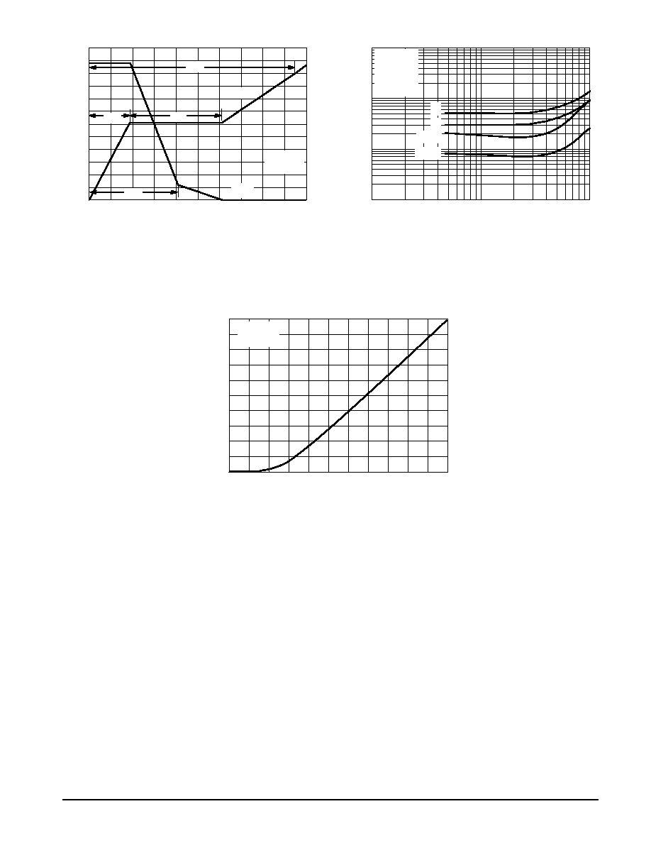
The resistive switching time variation versus gate resis-
tance (Figure 9) shows how typical switching performance is
affected by the parasitic circuit elements. If the parasitics
were not present, the slope of the curves would maintain a
value of unity regardless of the switching speed. The circuit
used to obtain the data is constructed to minimize common
inductance in the drain and gate circuit loops and is believed
readily achievable with board mounted components. Most
power electronic loads are inductive; the data in the figure is
taken with a resistive load, which approximates an optimally
snubbed inductive load. Power MOSFETs may be safely op-
erated into an inductive load; however, snubbing reduces
switching losses.
10
5
0
10
20
25
GATETOSOURCE OR DRAINTOSOURCE VOLTAGE (VOLTS)
C, CAP
ACIT
ANCE (pF)
Figure 7. Capacitance Variation
VGS
VDS
1500
1200
900
600
300
0
TJ = 25
°
C
VDS = 0 V
Ciss
Coss
Crss
5
15
VGS = 0 V
Ciss
Crss
MTD15N06V
5
Motorola TMOS Power MOSFET Transistor Device Data
V
DS
, DRAINT
OSOURCE VOL
T
AGE (VOL
TS)
V
GS
, GA
TET
OSOURCE VOL
T
AGE (VOL
TS)
DRAINTOSOURCE DIODE CHARACTERISTICS
0.5
0.7
0.9
1.1
1.3
1.5
VSD, SOURCETODRAIN VOLTAGE (VOLTS)
Figure 8. GateToSource and DrainToSource
Voltage versus Total Charge
I S
, SOURCE CURRENT
(AMPS)
Figure 9. Resistive Switching Time
Variation versus Gate Resistance
RG, GATE RESISTANCE (OHMS)
1
10
100
t,
TIME (ns)
VDD = 30 V
ID = 15 A
VGS = 10 V
TJ = 25
°
C
VGS = 0 V
TJ = 25
°
C
Figure 10. Diode Forward Voltage versus Current
0
QT, TOTAL CHARGE (nC)
3
6
9
12
15
ID = 15 A
TJ = 25
°
C
0
6
9
12
15
1000
100
10
1
10
6
2
0
12
8
4
60
50
40
30
20
10
0
tf
td(off)
td(on)
tr
VGS
Q2
3
Q3
QT
Q1
VDS
SAFE OPERATING AREA
The Forward Biased Safe Operating Area curves define
the maximum simultaneous draintosource voltage and
drain current that a transistor can handle safely when it is for-
ward biased. Curves are based upon maximum peak junc-
tion temperature and a case temperature (TC) of 25
°
C. Peak
repetitive pulsed power limits are determined by using the
thermal response data in conjunction with the procedures
discussed in AN569, "Transient Thermal ResistanceGeneral
Data and Its Use."
Switching between the offstate and the onstate may tra-
verse any load line provided neither rated peak current (IDM)
nor rated voltage (VDSS) is exceeded and the transition time
(tr,tf) do not exceed 10
µ
s. In addition the total power aver-
aged over a complete switching cycle must not exceed
(TJ(MAX) TC)/(R
JC).
A Power MOSFET designated EFET can be safely used
in switching circuits with unclamped inductive loads. For reli-
able operation, the stored energy from circuit inductance dis-
sipated in the transistor while in avalanche must be less than
the rated limit and adjusted for operating conditions differing
from those specified. Although industry practice is to rate in
terms of energy, avalanche energy capability is not a con-
stant. The energy rating decreases nonlinearly with an in-
crease of peak current in avalanche and peak junction
temperature.
Although many EFETs can withstand the stress of drain
tosource avalanche at currents up to rated pulsed current
(IDM), the energy rating is specified at rated continuous cur-
rent (ID), in accordance with industry custom. The energy rat-
ing must be derated for temperature as shown in the
accompanying graph (Figure 12). Maximum energy at cur-
rents below rated continuous ID can safely be assumed to
equal the values indicated.