1
MRF6404 MRF6404K
MOTOROLA RF DEVICE DATA
The RF Line
NPN Silicon
RF Power Transistor
The MRF6404 is designed for 26 volts microwave large signal, common
emitter, class AB linear amplifier applications operating in the range 1.8 to
2.0 GHz.
À
Specified 26 Volts, 1.88 GHz Characteristics
Output Power -- 30 Watts
Gain -- 7.5 dB Min @ 30 Watts
Efficiency -- 38% Min @ 30 Watts
À
Characterized with Series Equivalent Large¡Signal Parameters from
1.8 to 2.0 GHz
À
To be used in Class AB for DCS1800 and PCS1900/Cellular Radio
À
Gold Metallized, Emitter Ballasted for Long Life and Resistance to Metal
Migration
MAXIMUM RATINGS
Rating
Symbol
Value
Unit
Collector¡Emitter Voltage
VCEO
24
Vdc
Collector¡Emitter Voltage
VCES
60
Vdc
Emitter¡Base Voltage
VEBO
4
Vdc
Collector¡Current -- Continuous
IC
10
Adc
Total Device Dissipation @ TC = 25
░
C
Derate above 25
░
C
PD
125
0.71
Watts
W/
░
C
Storage Temperature Range
Tstg
¡ 65 to +150
░
C
Operating Junction Temperature
TJ
200
░
C
THERMAL CHARACTERISTICS
Characteristic
Symbol
Max
Unit
Thermal Resistance, Junction to Case (1)
R
JC
1.4
░
C/W
ELECTRICAL CHARACTERISTICS
(TC = 25
░
C unless otherwise noted)
Characteristic
Symbol
Min
Typ
Max
Unit
OFF CHARACTERISTICS
Collector¡Emitter Breakdown Voltage (IC = 50 mA, IB = 0)
V(BR)CEO
24
29
--
Vdc
Emitter¡Base Breakdown Voltage (IE = 10 mAdc)
V(BR)EBO
4
5
--
Vdc
Collector¡Base Breakdown Voltage (IC = 50 mAdc)
V(BR)CES
60
68
--
Vdc
Collector¡Base Breakdown Voltage (IC = 50 mAdc, RBE = 75
)
V(BR)CER
40
56
--
Vdc
Collector Cutoff Current (VCE = 30 V, VBE = 0)
ICES
--
--
10
mA
ON CHARACTERISTICS
DC Current Gain (IC = 1 Adc, VCE = 5 Vdc)
hFE
20
50
120
--
(1) Thermal resistance is determined under specified RF operating condition.
Order this document
by MRF6404/D
MOTOROLA
SEMICONDUCTOR TECHNICAL DATA
MRF6404
MRF6404K
30 W, 1.88 GHz
RF POWER TRANSISTOR
NPN SILICON
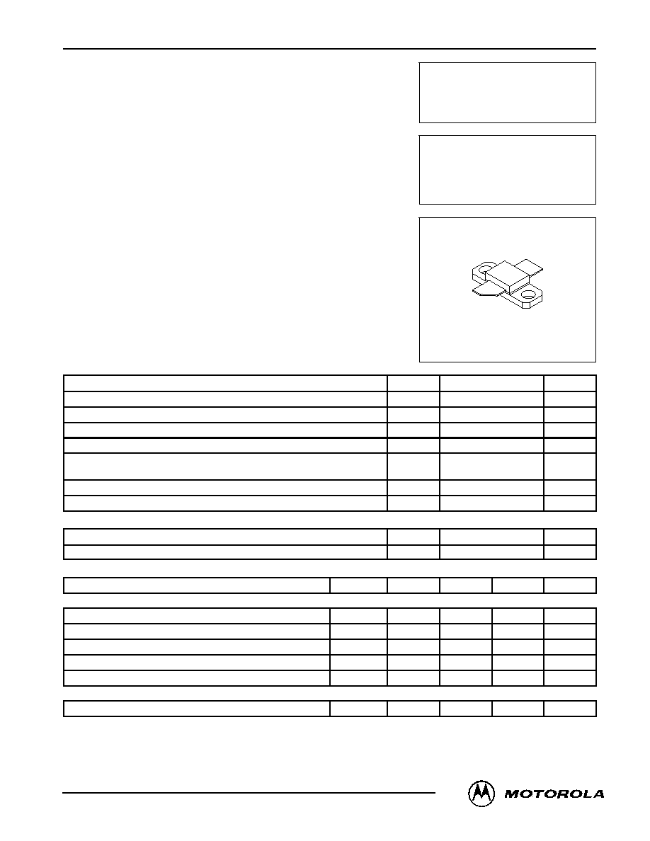
CASE 395C¡01, STYLE 1
®
Motorola, Inc. 1996
REV 2

MRF6404 MRF6404K
2
MOTOROLA RF DEVICE DATA
ELECTRICAL CHARACTERISTICS -- continued
(TC = 25
░
C unless otherwise noted)
Characteristic
Symbol
Min
Typ
Max
Unit
DYNAMIC CHARACTERISTICS
Output Capacitance
(VCB = 26 V, IE = 0, f = 1 MHz)
For information only. This part is collector matched.
Cob
30
38
--
pF
FUNCTIONAL TESTS
Common¡Emitter Amplifier Power Gain
(VCC = 26 V, Pout = 30 W, ICQ = 150 mA, f = 1.88 GHz)
Gpe
7.5
8.5
--
dB
Common¡Emitter Amplifier Power Gain
(VCC = 26 V, Pout = 28 W, ICQ = 150 mA)
(f = 1.99 GHz)
Gpe
7
8
--
dB
Collector Efficiency
(VCC = 26 V, Pout = 30 W, f = 1.88 GHz)
(VCC = 26 V, Pout = 28 W, f = 1.99 GHz)
38
35
43
40
--
--
%
Output Power at 1 dBc
(VCC = 26 V, f = 1.88 GHz)
(VCC = 26 V, f = 1.99 GHz)
P1dBc
30
28
35
33
--
--
Watts
Output Mismatch Stress: VSWR = 3:1 (all phase angles)
(VCC = 26 Vdc, Pout = 25 W, ICQ = 150 mA, f = 1.88 GHz)
No Degradation in Output Power
f
(GHz)
Zin
(
)
ZOL*
(
)
1.8
1.85
1.9
4.3 + j6.1
4.8 + j5.0
4.6 + j5.3
2.7 ¡ j1.0
2.9 + j0.3
3.0 + j1.2
ZOL*: Conjugate of optimum load impedance into
which the device operates at a given output
power, voltage, current and frequency.
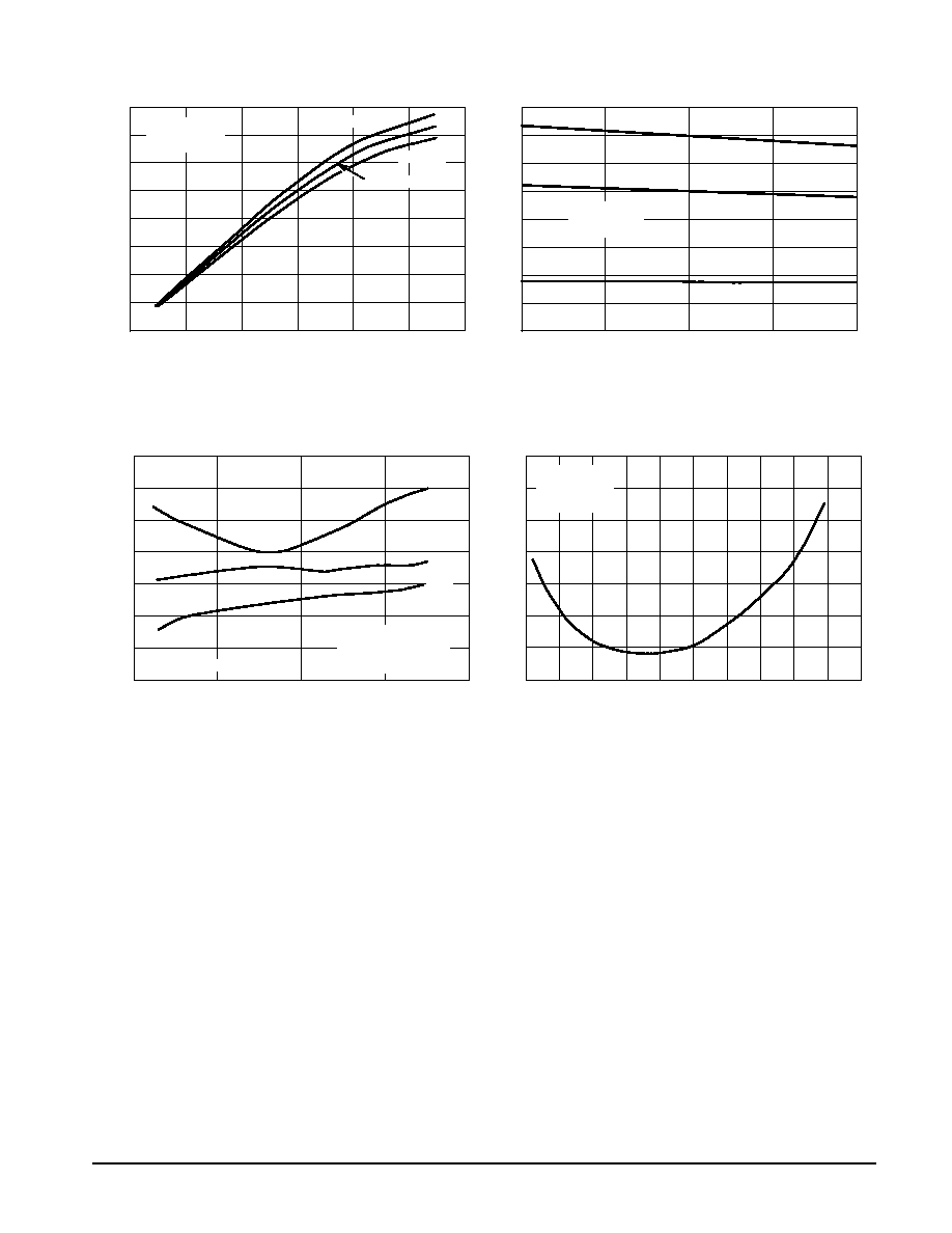
Figure 1. Input and Output Impedances with Circuit Tuned for Maximum Gain
@ VCC = 26 V, ICQ = 150 mA, Pout = 30 W
f = 1.8 GHz
1.9 GHz
ZOL*
Zin
f = 1.8 GHz
Zo = 20
1.9 GHz
DCS EVALUATION
3
MRF6404 MRF6404K
MOTOROLA RF DEVICE DATA
TYPICAL CHARACTERISTICS
1.9 GHz
1.8 GHz
f = 1.7 GHz
1 W
3 W
Pin = 5 W
7th
5th
3rd Order
PHASE (DEGREE)
Figure 2. Output Power versus Input Power
40
Pin, INPUT POWER (WATTS)
5
0
2
10
30
20
Figure 3. Output Power versus Frequency
1.80
f, FREQUENCY (GHz)
1.90
1
3
5
P out
, OUTPUT
POWER (W
A
TTS)
Figure 4. Intermodulation versus Output Power
Pout, OUTPUT POWER (WATTS) PEP
Figure 5. AM/PM Conversion
12
Pout, OUTPUT POWER (WATTS)
8
20
6
0
12
16
1.70
4
0
¡ 9
¡ 6
¡ 3
P out
, OUTPUT
POWER (W
A
TTS)
IMD, INTERMODULA
TION
DIST
OR
TION
(dBc)
4
6
1.85
1.75
¡ 60
20
40
¡ 35
¡ 45
¡ 25
0
¡ 55
¡ 40
¡ 50
¡ 30
30
10
36
28
35
25
15
40
5
0
10
30
20
35
25
15
9
3
32
24
40
0
VCC = 26 V
ICQ = 150 mA
VCC = 26 V
ICQ = 150 mA
f = 1.88 GHz
VCC = 26 V
ICQ = 150 mA
VCC = 26 V
ICQ= 150 mA
f = 1.88 & 1.8801 GHz
MRF6404 MRF6404K
4
MOTOROLA RF DEVICE DATA
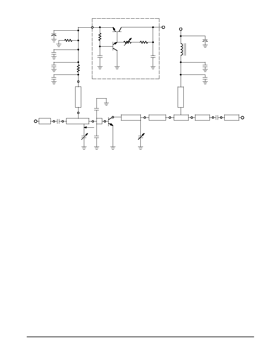
All Electrical Lengths Are Referenced from
g @ f = 1.9 GHz
Z1 : 50
1 : 10
░
Z2 : 50
2 : 74.5
░
B : 16.5
░
Z4 : 74
4 : 68
░
Z5 : 12.8
5 : 21
░
Z6 : 10.4
6 : 49.5
░
Z7 : 18
7 : 36.5
░
Z8 : 45
8 : 20
░
Z10 : 50
10 : 10
░
Z11 : 74
11 : 74.5
░
Z12 : 50
12 : 10
░
Figure 6. 1.80 ¡ 1.88 GHz Test Circuit Electrical Schematic and Components List
Base Bias Circuit
C12, C13
15 nF, Chip Capacitor, Vitramon (0805 A153 JXB)
P1
1 K
, Trimmer
R3
47
, Chip Resistor, 0805
R4
330
, Chip Resistor, 0805
T1,T2
Motorola MJD 31C
Decoupling Base Bias Circuit
C4
68 pF, Chip Capacitor, ATC 100A
C5, C9
330 pF, Chip Capacitor, Vitramon (0805 A331 JXB)
C7, C11
4.7
Á
F, 63 V, Electrolytic Capacitor
C8
68 pF, Chip Capacitor, ATC 100A
C10
15 nF, Chip Capacitor, Vitramon (0805 A153 JXB)
R1
1.5
, Chip Resistor, 0805
R2
56
, Chip Resistor, 1206
RF Circuit
C1, C2
68 pF, Chip Capacitor, ATC 100A
C20, C21
1.3 pF, Chip Capacitor, ATC 100A
CT2
Trimmer Capacitor, Gigatrim, Ref 37281
CT3
Trimmer Capacitor, Gigatrim, Ref 37291
TRF1
MRF6404
PC Board Material:
r = 2.55, H = 0.508 mm, T = 0.035 mm
L1
C4
C5
C7
VCC
RF
OUTPUT
C2
Z12,
12
Z10,
10
Z8,
8
RF CIRCUIT
Z7,
7
CT3
Z6,
6
TRF1
Z5,
5
C20
C21
CT2
B
Z2,
2
C1
RF
INPUT
Z1,
1
R1
C8
C9
C10
R2
C11
BASE BIAS CIRCUIT
T1
C12
R3
P1
C13
VBB
R4
T2
Z4
,
4
Z1
1
,
11
+
+
5
MRF6404 MRF6404K
MOTOROLA RF DEVICE DATA
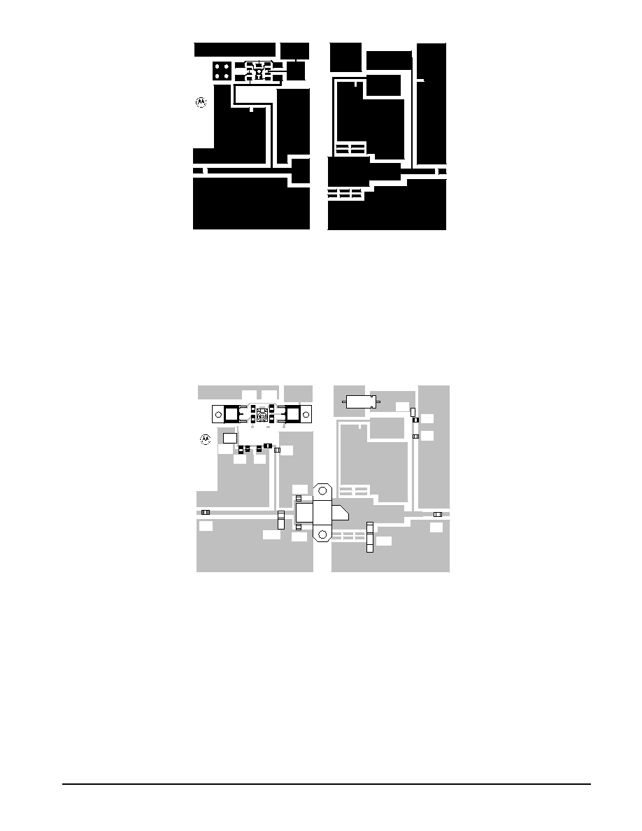
Figure 7. 1.80 ¡ 1.88 GHz PCN Test Circuit Photomaster
Teflon
«
Glass 0.5 mm ¡ Double Side 35
Á
m Cu.
(Not to Scale)
Figure 8. 1.80 ¡ 1.88 GHz PCN Test Circuit Components Layout
R1
C10
+VCC
RF INPUT
RF OUTPUT
T1
VBB
┬
┬
┬
┬
┬
┬
┬
C7
M
C13
C12
P1 R4
R3
R2
CT2
C1
C20
C8
C9
C21
C4
C5
C2
CT3
┬
┬
L1
C11
T1
T2