
1
MRF21120
MOTOROLA RF DEVICE DATA
The RF SubMicron MOSFET Line
RF Power Field Effect Transistor
NChannel EnhancementMode Lateral MOSFET
Designed for WCDMA base station applications with frequencies from 2110
to 2170 MHz. Suitable for FM, TDMA, CDMA and multicarrier amplifier
applications. To be used in Class AB for PCNPCS/cellular radio and WLL
applications.
· WCDMA Performance @ 45 dBc, 5 MHz Offset, 15 DTCH, 1 Perch
Output Power -- 14 Watts (Avg.)
Power Gain -- 11.5 dB
Efficiency -- 16%
· Internally Matched, Controlled Q, for Ease of Use
· High Gain, High Efficiency and High Linearity
· Integrated ESD Protection
· Designed for Maximum Gain and Insertion Phase Flatness
· Capable of Handling 10:1 VSWR, @ 28 Vdc, 2170 MHz, 120 Watts (CW)
Output Power
· Excellent Thermal Stability
· Characterized with Series Equivalent LargeSignal Impedance Parameters
MAXIMUM RATINGS
Rating
Symbol
Value
Unit
DrainSource Voltage
V
DSS
65
Vdc
GateSource Voltage
V
GS
0.5, +15
Vdc
Total Device Dissipation @ T
C
= 25
°C
Derate above 25
°C
P
D
389
2.22
Watts
W/
°C
Storage Temperature Range
T
stg
65 to +150
°C
Operating Junction Temperature
T
J
200
°C
ESD PROTECTION CHARACTERISTICS
Test Conditions
Class
Human Body Model
1 (Minimum)
Machine Model
M3 (Minimum)
THERMAL CHARACTERISTICS
Characteristic
Symbol
Max
Unit
Thermal Resistance, Junction to Case
R
JC
0.45
°C/W
NOTE CAUTION MOS devices are susceptible to damage from electrostatic charge. Reasonable precautions in handling and
packaging MOS devices should be observed.
Order this document
by MRF21120/D
MOTOROLA
SEMICONDUCTOR TECHNICAL DATA
MRF21120
2170 MHz, 120 W, 28 V
LATERAL NCHANNEL
RF POWER MOSFET
CASE 375D04, STYLE 1
NI1230
Motorola, Inc. 2002
REV 7

MRF21120
2
MOTOROLA RF DEVICE DATA
ELECTRICAL CHARACTERISTICS
(T
C
= 25
°C unless otherwise noted)
Characteristic
Symbol
Min
Typ
Max
Unit
OFF CHARACTERISTICS (1)
DrainSource Breakdown Voltage
(V
GS
= 0 Vdc, I
D
= 20
µAdc)
V
(BR)DSS
65
--
--
Vdc
GateSource Leakage Current
(V
GS
= 5 Vdc, V
DS
= 0 Vdc )
I
GSS
--
--
1
µAdc
Zero Gate Voltage Drain Leakage Current
(V
DS
= 28 Vdc, V
GS
= 0 Vdc)
I
DSS
--
--
10
µAdc
ON CHARACTERISTICS (1)
Forward Transconductance
(V
DS
= 10 Vdc, I
D
= 2 Adc)
g
fs
--
4.8
--
S
Gate Threshold Voltage
(V
DS
= 10 V, I
D
= 200
µA)
V
GS(th)
2.5
3
3.8
Vdc
Gate Quiescent Voltage
(V
DS
= 28 V, I
D
= 500 mA)
V
GS(Q)
3
3.9
5
Vdc
DrainSource OnVoltage
(V
GS
= 10 V, I
D
= 2 A)
V
DS(on)
--
0.38
0.5
Vdc
DYNAMIC CHARACTERISTICS (1)
Reverse Transfer Capacitance
(V
DS
= 28 Vdc, V
GS
= 0, f = 1 MHz)
C
rss
--
2.8
--
pF
FUNCTIONAL TESTS (In Motorola Test Fixture, 50 ohm system) (2)
CommonSource Amplifier Power Gain
(V
DD
= 28 Vdc, P
out
= 120 W PEP, I
DQ
= 2
500 mA,
f1 = 2170.0 MHz, f2 = 2170.1 MHz)
G
ps
10.5
11.4
--
dB
Drain Efficiency
(V
DD
= 28 Vdc, P
out
= 120 W PEP, I
DQ
= 2
500 mA,
f1 = 2170.0 MHz, f2 = 2170.1 MHz)
30
34.5
--
%
Intermodulation Distortion
(V
DD
= 28 Vdc, P
out
= 120 W PEP, I
DQ
= 2
500 mA,
f1 = 2170.0 MHz, f2 = 2170.1 MHz)
IMD
--
31
28
dB
Input Return Loss
(V
DD
= 28 Vdc, P
out
= 120 W PEP, I
DQ
= 2
500 mA,
f1 = 2170.0 MHz, f2 = 2170.1 MHz)
IRL
--
12
9
dB
CommonSource Amplifier Power Gain
(V
DD
= 28 Vdc, P
out
= 120 W PEP, I
DQ
= 2
500 mA,
f1 = 2140.0 MHz, f2 = 2140.1 MHz)
G
ps
--
11.5
--
dB
CommonSource Amplifier Power Gain
(V
DD
= 28 Vdc, P
out
= 120 W PEP, I
DQ
= 2
500 mA,
f1 = 2110.0 MHz, f2 = 2110.1 MHz)
G
ps
--
11.5
--
dB
Drain Efficiency
(V
DD
= 28 Vdc, P
out
= 120 W PEP, I
DQ
= 2
500 mA,
f1 = 2110.0 MHz, f2 = 2110.1 MHz)
--
34.5
--
%
Intermodulation Distortion
(V
DD
= 28 Vdc, P
out
= 120 W PEP, I
DQ
= 2
500 mA,
f1 = 2110.0 MHz, f2 = 2110.1 MHz)
IMD
--
31
--
dB
Input Return Loss
(V
DD
= 28 Vdc, P
out
= 120 W PEP, I
DQ
= 2
500 mA,
f1 = 2110.0 MHz, f2 = 2110.1 MHz)
IRL
--
12
--
dB
Power Output, 1 dB Compression Point
(V
DD
= 28 Vdc, CW, I
DQ
= 2
500 mA, f1 = 2170.0 MHz)
P1dB
--
120
--
Watts
(1) Each side of device measured separately.
(2) Device measured in pushpull configuration.

3
MRF21120
MOTOROLA RF DEVICE DATA
ELECTRICAL CHARACTERISTICS -- continued
(T
C
= 25
°C unless otherwise noted)
Characteristic
Symbol
Min
Typ
Max
Unit
FUNCTIONAL TESTS (In Motorola Test Fixture, 50 ohm system) (2) (continued)
CommonSource Amplifier Power Gain
(V
DD
= 28 Vdc, P
out
= 120 W CW, I
DQ
= 2
500 mA,
f1 = 2170.0 MHz)
G
ps
--
10.5
--
dB
Drain Efficiency
(V
DD
= 28 Vdc, P
out
= 120 W CW, I
DQ
= 2
500 mA,
f1 = 2170.0 MHz)
--
42
--
%
Output Mismatch Stress
(V
DD
= 28 Vdc, P
out
= 120 W CW, I
DQ
= 2
500 mA,
f = 2.17 GHz, VSWR = 10:1, All Phase Angles at Frequency of Tests)
No Degradation In Output Power
Before and After Test
(2) Device measured in pushpull configuration.
MRF21120
4
MOTOROLA RF DEVICE DATA
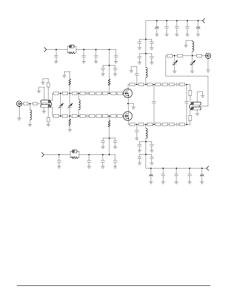
Figure 1. 2.1 2.2 GHz Broadband Test Circuit Schematic
V
GG
C19
C17
B1
C16
C14
+
V
DD
C33
+
C32
R3
C34
C35
+
Z1
Z10 Z12
Z14
Z18
Z20
DUT
C2
Z22
RF
INPUT
C3
COAX1
RF
OUTPUT
Z26
C9
Z28 Z30
Z34
C7
Z36
Z24
C8
COAX2
V
GG
C25
C24
C23
C21
+
COAX3
C6
V
DD
C42
C41
C40
+
C43
C44
+
COAX4
B1, B2
Ferrite Beads, Fair Rite
C1, C2, C12
0.6 4.5 pF Variable Capacitors, Johanson Gigatrim
C3, C4, C9, C10
10 pF Chip Capacitors, B Case, ATC
C5
0.4 2.5 pF Variable Capacitor, Johanson Gigatrim
C6, C7
2.0 pF Chip Capacitors, B Case, ATC
C8
0.5 pF Chip Capacitor, B Case, ATC
C11
0.2 pF Chip Capacitor, B Case, ATC
C13, C20, C29, C37
5.1 pF Chip Capacitors, B Case, ATC
C14, C21, C28, C38
91 pF Chip Capacitors, B Case, ATC
C15, C22, C27, C34, C36, C42 22
µF, 35 V Tantalum Surface Mount Chip Capacitors, Kemet
C16, C23, C33, C43
0.039
µF Chip Capacitors, B Case, ATC
C17, C24, C32, C41
1000 pF Chip Capacitors, B Case, ATC
C19, C25
0.022
µF Chip Capacitors, B Case, ATC
C30, C39
1.0
µF, 35 V Tantalum Surface Mount Chip Capacitors, Kemet
C31, C40
100
µF, 50 V Electrolytic Capacitors, Sprague
C35, C44
470
µF, 63 V Electrolytic Capacitors, Sprague
Coax1, Coax2
25
Semi Rigid Coax, 70 mil OD, 1.05 Long
Coax3, Coax4
50
Semi Rigid Coax, 85 mil OD, 1.05 Long
L1, L5
5.0 nH Minispring Inductors, Coilcraft
L2
8.0 nH Minispring Inductor, Coilcraft
L3, L4
7.15 nH Microspring Inductors, Coilcraft
R1, R2
1 k
, 1/4 W Fixed Metal Film Resistors, Dale
R3, R4
270
, 1/8 W Fixed Film Chip Resistors, Dale
R5, R6
1.2 k
, 1/8 W Fixed Film Chip Resistors, Dale
Z1
0.150
x 0.080 Microstrip
Z2
0.320
x 0.080 Microstrip
Z4, Z5
1.050
x 0.080 Microstrip
Z6, Z7
0.120
x 0.080 Microstrip
Z8, Z9
0.140
x 0.080 Microstrip
Z10, Z11
0.610
x 0.080 Microstrip
Z12, Z13
0.135
x 0.080 Microstrip
Z14, Z15
0.130
x 0.080 Microstrip
Z16, Z17
0.300
x 0.350 Microstrip
Z18, Z19
0.150
x 0.500 Microstrip
Z20, Z21
0.075
x 0.500 Microstrip
Z22, Z23
0.330
x 0.500 Microstrip
Z24, Z25
0.100
x 0.550 Microstrip
Z26, Z27
0.175
x 0.550 Microstrip
Z28, Z29
0.045
x 0.550 Microstrip
Z30, Z31
0.190
x 0.325 Microstrip
Z32, Z33
0.080
x 0.325 Microstrip
Z34, Z35
0.515
x 0.080 Microstrip
Z36, Z37
0.020
x 0.080 Microstrip
Z38, Z39
0.565
x 0.080 Microstrip
Z40
0.100
x 0.080 Microstrip
Z41
0.470
x 0.080 Microstrip
Z42
0.100
x 0.080 Microstrip
Board Material
0.03
Teflon
,
r
= 2.55 Copper
Clad, 2 oz. Cu
Connectors
NType Panel Mount, Stripline
C13
C15
R5
L2
Z8
C1
Z6
Z2
Z4
Z5
L1
Z16
Z11 Z13
Z15
Z19
Z21 Z23
C4
Z9
Z7
Z17
R6
C20
C22
B2
R4
C31
C27
C29
C28
C30
Z32
C11
Z38
Z39
L4
Z27
C10
Z29 Z31
Z35
Z37
Z25
Z33
C36
C37
C38
C39
Z42
L5
Z41
C12
Z40
+
+
L3
R1
R2
C5
+
+
+
+
+
+
+
+

5
MRF21120
MOTOROLA RF DEVICE DATA
Figure 2. 2.1 2.2 GHz Broadband Test Circuit Component Layout
L1
R1
C19
B1
R3
R5
C1 C2
R2
L2
C3
C4
R6
R4
B2
C25
V
GG
C24
C23
C22
C21
C20
C17
C16
C15
C14
C13
C30
C29
C7
L3
L4
C8
C6
C37
C39
C38
C36
C40
C42
C44
V
DD
C41 C43
C9
C10
C11
C12
C5
L5
C27
C32 C33
V
DD
V
GG
C31
C34
C35
226
35K
649
226
35K
649
226
35K
649
226
35K
649
226 35K 649
640
50K
105
226 35K 649
C28
640
50K
105