1
MRF19045R3 MRF19045SR3
MOTOROLA RF DEVICE DATA
The RF MOSFET Line
RF Power Field Effect Transistors
NChannel EnhancementMode Lateral MOSFETs
Designed for PCN and PCS base station applications with frequencies from
1 . 9 t o 2 . 0 G H z . S u i t a b l e f o r T D M A , C D M A a n d m u l t i c a r r i e r a m p l i f i e r
applications.
· Typical CDMA Performance @ 1960 MHz, 26 Volts, I
DQ
= 550 mA
Multicarrier CDMA Pilot, Sync, Paging, Traffic Codes 8 Through 13
Output Power -- 9.5 Watts Avg.
Power Gain -- 14.9 dB
Efficiency -- 23.5%
Adjacent Channel Power --
885 kHz: 50 dBc @ 30 kHz BW
IM3 -- 37 dBc
· 100% Tested Under 2Carrier NCDMA
· Internally Matched, Controlled Q, for Ease of Use
· High Gain, High Efficiency and High Linearity
· Integrated ESD Protection
· Designed for Maximum Gain and Insertion Phase Flatness
· Capable of Handling 5:1 VSWR, @ 26 Vdc, 1.93 GHz, 45 Watts CW
Output Power
· Excellent Thermal Stability
· Characterized with Series Equivalent LargeSignal Impedance Parameters
· In Tape and Reel. R3 Suffix = 250 Units per 32 mm, 13 Inch Reel.
MAXIMUM RATINGS
Rating
Symbol
Value
Unit
DrainSource Voltage
V
DSS
65
Vdc
GateSource Voltage
V
GS
0.5, +15
Vdc
Total Device Dissipation @ T
C
= 25
°C
Derate above 25
°C
P
D
105
0.60
Watts
W/
°C
Storage Temperature Range
T
stg
65 to +200
°C
Operating Junction Temperature
T
J
200
°C
ESD PROTECTION CHARACTERISTICS
Test Conditions
Class
Human Body Model
2 (Minimum)
Machine Model
M3 (Minimum)
THERMAL CHARACTERISTICS
Characteristic
Symbol
Max
Unit
Thermal Resistance, Junction to Case
R
JC
1.65
°C/W
NOTE CAUTION MOS devices are susceptible to damage from electrostatic charge. Reasonable precautions in handling and
packaging MOS devices should be observed.
Order this document
by MRF19045/D
MOTOROLA
SEMICONDUCTOR TECHNICAL DATA
MRF19045R3
MRF19045SR3
1990 MHz, 45 W, 26 V
LATERAL NCHANNEL
RF POWER MOSFETs
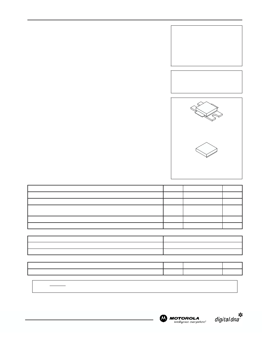
CASE 465E03, STYLE 1
NI400
MRF19045R3
CASE 465F03, STYLE 1
NI400S
MRF19045SR3
Motorola, Inc. 2002
REV 3
MRF19045R3 MRF19045SR3
2
MOTOROLA RF DEVICE DATA
ELECTRICAL CHARACTERISTICS
(T
C
= 25
°C unless otherwise noted)
Characteristic
Symbol
Min
Typ
Max
Unit
OFF CHARACTERISTICS
DrainSource Breakdown Voltage
(V
GS
= 0 Vdc, I
D
= 100
µAdc)
V
(BR)DSS
65
--
--
Vdc
Zero Gate Voltage Drain Current
(V
DS
= 26 Vdc, V
GS
= 0 Vdc)
I
DSS
--
--
10
µAdc
GateSource Leakage Current
(V
GS
= 5 Vdc, V
DS
= 0 Vdc)
I
GSS
--
--
1
µAdc
ON CHARACTERISTICS (DC)
Gate Threshold Voltage
(V
DS
= 10 Vdc, I
D
= 100
µAdc)
V
GS(th)
2
--
4
Vdc
Gate Quiescent Voltage
(V
DS
= 26 Vdc, I
D
= 550 mAdc)
V
GS(Q)
3
3.8
5
Vdc
DrainSource OnVoltage
(V
GS
= 10 Vdc, I
D
= 1 Adc)
V
DS(on)
--
0.19
0.21
Vdc
Forward Transconductance
(V
DS
= 10 Vdc, I
D
= 2 Adc)
g
fs
--
4.2
--
S
DYNAMIC CHARACTERISTICS
Reverse Transfer Capacitance (1)
(V
DS
= 26 Vdc, V
GS
= 0, f = 1.0 MHz)
C
rss
--
1.8
--
pF
FUNCTIONAL TESTS (In Motorola Test Fixture, 50 ohm system) 2carrier NCDMA, 1.2288 MHz Channel Bandwidth, IM3 measured in
1.2288 MHz Integrated Bandwidth. ACPR measured in 30 kHz Integrated Bandwidth.
CommonSource Amplifier Power Gain
(V
DD
= 26 Vdc, P
out
= 9.5 W Avg, 2Carrier NCDMA,
I
DQ
= 550 mA, f1 = 1930 MHz, f2 = 1932.5 MHz and f1 =1987.5 MHz,
f2 = 1990 MHz)
G
ps
13
14.5
--
dB
Drain Efficiency
(V
DD
= 26 Vdc, P
out
= 9.5 W Avg, 2Carrier NCDMA,
I
DQ
= 550 mA, f1 = 1930 MHz, f2 = 1932.5 MHz and f1 =1987.5 MHz,
f2 = 1990 MHz)
21
23.5
--
%
3rd Order Intermodulation Distortion
(V
DD
= 26 Vdc, P
out
= 9.5 W Avg, 2Carrier NCDMA,
I
DQ
= 550 mA, f1 = 1930 MHz, f2 = 1932.5 MHz and f1 =1987.5 MHz,
f2 = 1990 MHz; IM3 Measured in a 1.2288 MHz Integrated Bandwidth
Centered at f1 2.5 Mhz and f2 +2.5 MHz, Referenced to the Carrier
Channel Power)
IM3
--
37
35
dBc
Adjacent Channel Power Ratio
(V
DD
= 26 Vdc, P
out
= 9.5 W Avg, 2carrier NCDMA, I
DQ
= 550 mA,
f1 = 1930 MHz, f2 = 1932.5 MHz and f1 = 1987.5 MHz,
f2 = 1990 MHz; ACPR measured in a 30 kHz Integrated Bandwith
Centered at f1 885 kHz and f2 +885 kHz)
ACPR
--
51
45
dBc
Input Return Loss
(V
DD
= 26 Vdc, P
out
= 9.5 W Avg, 2Carrier NCDMA,
I
DQ
= 550 mA, f1 = 1930 MHz, f2 = 1932.5 MHz and f1 =1987.5 MHz,
f2 = 1990 MHz)
IRL
--
16
9
dB
P
out
, 1 dB Compression Point
(V
DD
= 26 Vdc, I
DQ
= 550 mA, f = 1990 MHz)
P1dB
--
45
--
W
Output Mismatch Stress
(V
DD
= 26 Vdc, P
out
= 45 W CW, I
DQ
= 550 mA,
f = 1930 MHz, VSWR = 5:1, All Phase Angles at Frequency of Tests)
No Degradation In Output Power
Before and After Test
(1) Part is internally matched both on input and output.

3
MRF19045R3 MRF19045SR3
MOTOROLA RF DEVICE DATA
Figure 1. 1930 1990 MHz 2-Carrier N-CDMA Test Circuit Schematic
RF
OUTPUT
Z3
Z4
C6
C1
R1
C3
+
C7
C5
C8
C2
Z6
Z7
V
DD
C12
C10
Z11
C9
Z8
C11
+
Z9
0.519
x 0.254 Microstrip
Z10
0.874
x 0.081 Microstrip
Z11
0.645
x 0.081 Microstrip
Board
3
x 5 Copper Clad PCB,
Arlon GX0300-55-22,
r
= 2.55
Printed Circuit
CMR Part Number 19045PC5.SKF
Board
Z1
1.336
x 0.081 Microstrip
Z2
0.693
x 0.081 Microstrip
Z3
1.033
x 0.047 Microstrip
Z4
0.468
x 0.047 Microstrip
Z5
0.271
x 0.460 Microstrip
Z6
0.263
x 0.930 Microstrip
Z7
1.165
x 0.047 Microstrip
Z8
0.216
x 0.047 Microstrip
NOTE: Z3, Z4, Z7, Z8 lengths and component placement tolerances are
±0.050.
Zx lengths are microstrip lengths between components, center-line to center-line.
All component and z-length tolerances are
±0.015, except as noted.
+
+
V
GG
RF
INPUT
Z1
Z2
Z5
W2
R4
+
Z9
Z10
C13
B2
R5
B2
W1
R3
B1
R2
C4
Table 1. 1930 1990 MHz 2-Carrier N-CDMA Test Circuit Component Designations and Values
Designators
Description
B1, B2
0.120
x 0.333 x 0.100, Surface Mount Ferrite Beads, Fair Rite #2743019446
C1, C2
10
mF, 35 V Tantalum Surface Mount Chip Capacitors, Kemet #T495X106K035AS4394
C3, C11
0.1
mF Chip Capacitors, Kemet #CDR33BX104AKWS
C4, C8
24 pF Chip Capacitors, B Case, ATC #100B240JP500X
C5
470 pF Chip Capacitor, B Case, ATC #100B471JP200X
C6, C7
11 pF Chip Capacitors, B Case, ATC #100B110JP500X
C9, C10, C12
22
mF, 35 V Tantalum Surface Mount Chip Capacitors, Kemet #T491X226K035AS4394
C13
8.2 pF Chip Capacitor, B Case, ATC #100B8R2CP500X
R1
560 k
, 1/4 W Chip Resistor (0.08 x 0.13)
R2, R3, R4, R5
8.2
, 1/4 W Chip Resistors (0.08 x 0.13), Garrett Instruments #RM73B2B110JT
W1, W2
Solid Copper Buss Wire, 16 AWG
WS1, WS2
Beryllium Copper Wear Blocks (0.005
x 0.150 x 0.350) Nominal
Brass Banana Jack and Nut
Red Banana Jack and Nut
Green Banana Jack and Nut
Type "N" Jack Connectors, Omni-Spectra #3052-1648-10
4-40 Ph Head Screws, 0.125
long
4-40 Ph Head Screws, 0.312
long
4-40 Ph Head Screws, 0.625
long
4-40 Ph Rec. Hd. Screws, 0.625
long

MRF19045R3 MRF19045SR3
4
MOTOROLA RF DEVICE DATA
Figure 2. 1930 1990 MHz 2-Carrier N-CDMA Test Circuit Component Layout
C1
C13
C12
W1
WS1
W2
B1
R1
R2
R3
R4
R5
B2
C2
C3
C4
C5
C6
C7 C8
C9 C10
MRF19045/S
Rev0
C11
WS2
5
MRF19045R3 MRF19045SR3
MOTOROLA RF DEVICE DATA
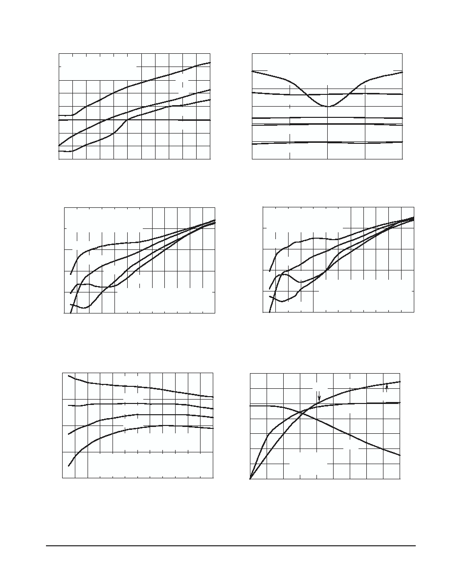
TYPICAL CHARACTERISTICS
5
10
15
20
25
30
35
1900
1930
1960
1990
2020
-60
-50
-40
-30
-20
-10
0
Figure 3. 2-Carrier NCDMA ACPR, IM3, Power Gain
and Drain Efficiency versus Output Power
Figure 4. 2-Carrier N-CDMA ACPR, IM3, Power Gain, IRL
and Drain Efficiency versus Output Power
Figure 5. 2-Carrier N-CDMA IM3
versus Output Power
P
out
, OUTPUT POWER (WATTS) (Avg. 2 Carrier N CDMA)
Figure 6. 2-Carrier N-CDMA ACPR
versus Output Power
13.5
ACPR,
ADJACENT
CHANNEL
POWER RA
TIO (dBc)
G
ps
, POWER GAIN (dB)
IM3,
THIRD ORDER
INTERMODULA
TION DIST
OR
TION (dBc)
, DRAIN EFFICIENCY
(%),
G
ps
, POWER GAIN (dB)
P
out
, OUTPUT POWER (WATTS) (Avg. 2 Carrier N CDMA)
IM3 (dBc),
ACPR (dBc)
0
5
10
15
20
25
30
35
40
1
2
3
4
5
6
7
8
9
10
11
12
-70
-65
-60
-55
-50
-45
-40
-35
-30
G
ps
ACPR
IM3
G
ps
ACPR
IM3
IRL
f, FREQUENCY (MHz)
IM3 (dBc),
ACPR (dBc),
IRL
(dB)
, DRAIN EFFICIENCY
(%),
G
ps
, POWER GAIN (dB)
-55
-50
-45
-40
-35
-30
0
1
9
10 11 12
350 mA
450 mA
700 mA
550 mA
V
DD
= 26 Vdc
I
DQ
= 550 mA
f1 = 1960 MHz, f2 = 1962.5 MHz
2
3
4
5
6
7
8
P
out
, OUTPUT POWER (WATTS) (Avg. 2 Carrier N CDMA)
0
1
9
10 11 12
2
3
4
5
6
7
8
-70
-55
-65
-60
-50
-45
Figure 7. 2-Carrier N-CDMA Power Gain
versus Output Power
P
out
, OUTPUT POWER (WATTS) (Avg. 2 Carrier N CDMA)
350 mA
450 mA
700 mA
550 mA
0
1
9
10 11 12
2
3
4
5
6
7
8
350 mA
450 mA
700 mA
550 mA
14.0
14.5
15.0
15.5
V
DD
= 26 Vdc
I
DQ
= 450 mA
f1 = 1960 MHz, f2 = 1960.1 MHz
1.2288 MHz Source Channel Bandwidth,
9 CH FWD Carrier
(9.8 dB Peak/Avg. Ratio @ 0.01%)
V
DD
= 26 Vdc, I
DQ
= 550 mA 2.5 MHz Carrier Spacing
9 CH FWD Carrier (9.8 dB Peak/Avg. Ratio @ 0.01%)
1.2288 MHz Source Channel Bandwidth
V
DD
= 26 Vdc
I
DQ
= 550 mA
f1 = 1960 MHz, f2 = 1962.5 MHz
1.2288 MHz Source Channel Bandwidth,
9 CH FWD Carrier
(9.8 dB Peak/Avg. Ratio @ 0.01%
Probability) (CCDF)
V
DD
= 26 Vdc, I
DQ
= 550 mA
f1 = 1960 MHz, f2 = 1962.5 MHz
1.2288 MHz Source Channel Bandwidth,
9 CH FWD Carrier
(9.8 dB Peak/Avg. Ratio @ 0.01% Probability) (CCDF)
Figure 8. CW Output Power, Power Gain and Drain
Efficiency versus Input Power
0
10
20
30
40
50
60
70
0.0
0.5
1.0
1.5
2.0
2.5
3.0
3.5
4.0
4.5
10
11
12
13
14
15
16
17
Gps
Pout
P1dB
P3dB
P
in
, INPUT POWER (WATTS CW)
, DRAIN EFFICIENCY
(%),
P
, OUTPUT
POWER (W
A
TTS CW)
out
G
ps
, POWER GAIN (dB)
V
DD
= 26 Vdc
I
DQ
= 550 mA
f = 1960 MHz