MRF18085AR3 MRF18085ALSR3
5 - 1
RF Device Data
Freescale Semiconductor
RF Power Field Effect Transistors
N - Channel Enhancement - Mode Lateral MOSFETs
D e s i g n e d f o r G S M a n d G S M E D G E b a s e s t a t i o n a p p l i c a t i o n s w i t h
f r e q u e n c i e s f r o m 1 8 0 0 t o 2 0 0 0 M H z . S u i t a b l e f o r T D M A , C D M A a n d
multicarrier amplifier applications. To be used in Class AB for PCN - PCS/
c e l l u l a r r a d i o a n d W L L a p p l i c a t i o n s . S p e c i f i e d f o r G S M - G S M E D G E
1805 - 1880 MHz.
· GSM and GSM EDGE Performance, Full Frequency Band
(1805 - 1880 MHz)
Power Gain - 15 dB (Typ) @ 85 Watts CW
Efficiency - 52% (Typ) @ 85 Watts CW
· Internally Matched, Controlled Q, for Ease of Use
· High Gain, High Efficiency and High Linearity
· Integrated ESD Protection
· Designed for Maximum Gain and Insertion Phase Flatness
· Capable of Handling 5:1 VSWR, @ 26 Vdc, @ P1dB Output Power,
@ f = 1805 MHz
· Excellent Thermal Stability
· Characterized with Series Equivalent Large-Signal Impedance Parameters
· Available with Low Gold Plating Thickness on Leads. L Suffix Indicates
40
µ Nominal.
· In Tape and Reel. R3 Suffix = 250 Units per 56 mm, 13 inch Reel.
Table 1. Maximum Ratings
Rating
Symbol
Value
Unit
Drain - Source Voltage
V
DSS
- 0.5, +65
Vdc
Gate - Source Voltage
V
GS
- 0.5, +15
Vdc
Total Device Dissipation @ T
C
= 25
°C
Derate above 25
°C
P
D
273
1.56
W
W/
°C
Storage Temperature Range
T
stg
- 65 to +150
°C
Operating Junction Temperature
T
J
200
°C
Table 2. Thermal Characteristics
Characteristic
Symbol
Value
(1)
Unit
Thermal Resistance, Junction to Case
R
JC
0.79
°C/W
Table 3. ESD Protection Characteristics
Test Conditions
Class
Human Body Model
1 (Minimum)
Machine Model
M3 (Minimum)
1. Refer to AN1955/D, Thermal Measurement Methodology of RF Power Amplifiers. Go to http://www.freescale.com/rf.
Select Documentation/Application Notes - AN1955.
NOTE - CAUTION - MOS devices are susceptible to damage from electrostatic charge. Reasonable precautions in handling and
packaging MOS devices should be observed.
MRF18085A
Rev. 4, 12/2004
Freescale Semiconductor
Technical Data
MRF18085AR3
MRF18085ALSR3
1800 - 1880 MHz, 85 W, 26 V
GSM/GSM EDGE
LATERAL N - CHANNEL
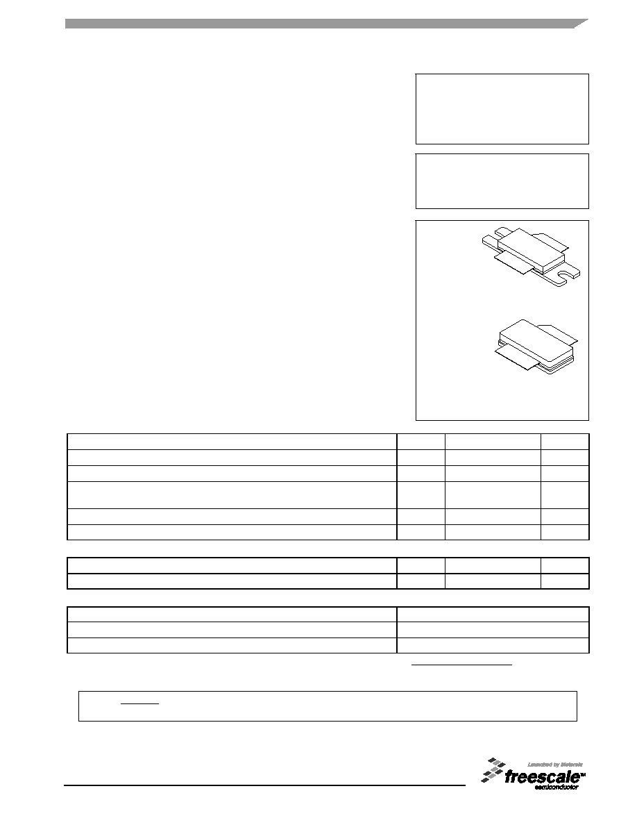
RF POWER MOSFETs
CASE 465 - 06, STYLE 1
NI - 780
MRF18085AR3
CASE 465A - 06, STYLE 1
NI - 780S
MRF18085ALSR3
Freescale Semiconductor, Inc., 2004. All rights reserved.

5 - 2
RF Device Data
Freescale Semiconductor
MRF18085AR3 MRF18085ALSR3
Table 4. Electrical Characteristics
(T
C
= 25
°C unless otherwise noted)
Characteristic
Symbol
Min
Typ
Max
Unit
Off Characteristics
Drain - Source Breakdown Voltage
(V
GS
= 0 Vdc, I
D
= 100
µAdc)
V
(BR)DSS
65
--
--
Vdc
Zero Gate Voltage Drain Current
(V
DS
= 26 Vdc, V
GS
= 0 Vdc)
I
DSS
--
--
10
µAdc
Gate - Source Leakage Current
(V
GS
= 5 Vdc, V
DS
= 0 Vdc)
I
GSS
--
--
1
µAdc
On Characteristics
Gate Threshold Voltage
(V
DS
= 10 Vdc, I
D
= 200
µAdc)
V
GS(th)
2
--
4
Vdc
Gate Quiescent Voltage
(V
DS
= 26 Vdc, I
D
= 600 mAdc)
V
GS(Q)
2.5
3.9
4.5
Vdc
Drain - Source On - Voltage
(V
GS
= 10 Vdc, I
D
= 2 Adc)
V
DS(on)
--
0.15
--
Vdc
Forward Transconductance
(V
DS
= 10 Vdc, I
D
= 2 Adc)
g
fs
--
6.0
--
S
Dynamic Characteristics
Reverse Transfer Capacitance
(1)
(V
DS
= 26 Vdc, V
GS
= 0, f = 1 MHz)
C
rss
--
3.6
--
pF
Functional Tests (In Freescale Test Fixture, 50 ohm system)
Common- Source Amplifier Power Gain @ 85 W
(2)
(V
DD
= 26 Vdc, I
DQ
= 800 mA, f = 1805 - 1880 MHz)
G
ps
13.5
15
--
dB
Drain Efficiency @ 85 W
(2)
(V
DD
= 26 Vdc, I
DQ
= 800 mA, f = 1805 - 1880 MHz)
48
52
--
%
Input Return Loss @ 85 W
(2)
(V
DD
= 26 Vdc, I
DQ
= 800 mA, f = 1805 - 1880 MHz)
IRL
--
- 12
- 9
dB
Power Output, 1 dB Compression Point
(V
DD
= 26 Vdc, I
DQ
= 800 mA, f = 1805 - 1880 MHz)
P1dB
83
90
--
Watts
Output Mismatch Stress @ P1dB
(V
DD
= 26 Vdc, I
DQ
= 800 mA, f = 1805 MHz,
VSWR = 5:1, All Phase Angles at Frequency of Tests)
No Degradation In Output Power
Before and After Test
1. Part is internally matched both on input and output.
2. To meet application requirements, Freescale test fixtures have been designed to cover the full GSM1800 band, ensuring
batch - to - batch consistency.

MRF18085AR3 MRF18085ALSR3
5 - 3
RF Device Data
Freescale Semiconductor
V
BIAS
C1, C3, C6, C7
10 pF Chip Capacitors, ATC
C2
1.8 pF Chip Capacitor, ATC
C4
10
mF, 35 V Tantalum Capacitor, AVX
C5, C8
1 nF Chip Capacitors, ATC
C9
220
mF, 63 V Electrolytic Capacitor, Radial, Philips
C10
0.3 pF Chip Capacitor, ATC
R1, R2
10 k
W, 1/4 W Chip Resistors (1206)
R3
1.0 k
W, 1/4 W Chip Resistor (1206)
Z1
0.671
x 0.087 Microstrip
Z2
0.568
x 0.087 Microstrip
Z3
0.500
x 0.098 Microstrip Shorted Stub
Z4
0.610
x 00.118 Microstrip
Z5
0.331
x 1.153 Microstrip
Z6
0.063
x 1.153 Microstrip
Z7
0.122
x 0.925 Microstrip
Z8
0.547
x 0.925 Microstrip
Z9
0.394
x 0.177 Microstrip
Z10
0.180
x 0.087 Microstrip
Z11
0.686
x 0.087 Microstrip
Z12
0.294
x 0.087 Microstrip
PCB
Taconic TLX8, 30 mils,
r
= 2.55
Figure 1. 1800 - 1880 MHz Test Fixture Schematic
RF
INPUT
RF
OUTPUT
Z1
C1
C3
C5
Z5
DUT
Z9
Z10
Z12
C6
R3
C9
+
Z4
R1
C4
C8
V
SUPPLY
R2
+
C2
Z8
C7
Z3
Z2
C10
Z6
Z7
Z11
Figure 2. 1800 - 1880 MHz Test Fixture Component Layout
MRF18085A
C - PP - 02 - 01 - 2 - Rev0
CUT
OUT
AREA
C9
Strap
C4
R1
R2
C5 C6
R3
C2
C1
C3
C7
C8
C10
Freescale has begun the transition of marking Printed Circuit Boards (PCBs) with the Freescale Semiconductor
signature/logo. PCBs may have either Motorola or Freescale markings during the transition period. These changes will have
no impact on form, fit or function of the current product.

5 - 4
RF Device Data
Freescale Semiconductor
MRF18085AR3 MRF18085ALSR3
TYPICAL CHARACTERISTICS
1000
10
17
0
P
out
, OUTPUT POWER (WATTS)
Figure 3. Power Gain versus Output Power
G
ps
, POWER GAIN (dB)
16
15
14
13
12
11
1
10
100
P
out
, OUTPUT POWER (WATTS)
Figure 4. Power Gain versus Output Power
G
ps
, POWER GAIN (dB)
1000
9
17
1
T
C
= 25
_C
50
_C
P
out
, OUTPUT POWER (WATTS)
Figure 5. Power Gain versus Output Power
G
ps
, POWER GAIN (dB)
V
DD
= 26 Vdc
I
DQ
= 800 mA
f = 1840 MHz
100
10
16
15
14
13
12
11
10
85
_C
1900
0
120
1800
P
in
= 8 W
f, FREQUENCY (MHz)
Figure 6. Output Power versus Frequency
P
out
, OUTPUT
POWER (W
A
TTS)
V
DD
= 26 Vdc
I
DQ
= 800 mA
T
C
= 25
_C
4 W
1 W
0.5 W
100
80
60
40
20
1820
1840
1860
1880
1950
10
17
1750
-28
0
G
ps
@ 30 W
f, FREQUENCY (MHz)
Figure 7. Power Gain versus Frequency
G
ps
, POWER GAIN (dB)
INPUT
RETURN LOSS (dB)
IRL,
V
DD
= 26 Vdc
I
DQ
= 800 mA
T
C
= 25
_C
G
ps
@ 80 W
IRL @ 80 W
IRL @ 30 W
16
-4
15
-8
14
-12
13
-16
12
-20
11
-24
1800
1850
1900
1000
10
16
0.1
0
60
G
ps
P
out
, OUTPUT POWER (WATTS)
Figure 8. Power Gain and Efficiency versus
Output Power
G
ps
, POWER GAIN (dB)
, DRAIN EFFICIENCY
(%)
V
DD
= 26 Vdc
I
DQ
= 800 mA
f = 1840 MHz
T
C
= 25
_C
15
50
14
40
13
30
12
20
11
10
1
10
100
1000
8
17
0.1
24 V
I
DQ
= 800 mA
f = 1840 MHz
T
C
= 25
_C
16
15
14
13
12
11
10
9
1
10
100
V
DD
= 20 V
28 V
32 V
I
DQ
= 1000 mA
V
DD
= 26 Vdc
f = 1840 MHz
T
C
= 25
_C
800 mA
600 mA
400 mA

MRF18085AR3 MRF18085ALSR3
5 - 5
RF Device Data
Freescale Semiconductor
Figure 9. Series Equivalent Source and Load Impedance
f
MHz
Z
source
Z
load
1710
1785
1.13 - j3.62
1.69 - j4.34
1.61 - j4.23
1.79 - j2.88
1.82 - j3.15
1.90 - j2.66
V
DD
= 26 V, I
DQ
= 800 mA, P
out
= 85
W CW
Z
o
= 10
f = 1990 MHz
f = 1990 MHz
f = 1710 MHz
f = 1710 MHz
1805
1880
2.83 - j5.25
2.09 - j2.77
1930
4.39 - j4.97
3.00 - j5.18
2.01 - j2.44
2.01 - j2.57
1960
1990
6.59 - j4.74
1.79 - j2.37
Z
source
Z
source
= Test circuit impedance as measured from
gate to ground.
Z
load
= Test circuit impedance as measured
from drain to ground.
Z source
Z load
Input
Matching
Network
Device
Under Test
Output
Matching
Network
Z
load