1
MRF141G
MOTOROLA RF DEVICE DATA
The RF MOSFET Line
RF Power Field-Effect Transistor
N¡Channel Enhancement¡Mode MOSFET
Designed for broadband commercial and military applications at frequencies
to 175 MHz. The high power, high gain and broadband performance of this
device makes possible solid state transmitters for FM broadcast or TV channel
frequency bands.
À
Guaranteed Performance at 175 MHz, 28 V:
Output Power -- 300 W
Gain -- 12 dB (14 dB Typ)
Efficiency -- 50%
À
Low Thermal Resistance -- 0.35
░
C/W
À
Ruggedness Tested at Rated Output Power
À
Nitride Passivated Die for Enhanced Reliability
MAXIMUM RATINGS
Rating
Symbol
Value
Unit
Drain¡Source Voltage
VDSS
65
Vdc
Drain¡Gate Voltage
VDGO
65
Vdc
Gate¡Source Voltage
VGS
▒
40
Vdc
Drain Current -- Continuous
ID
32
Adc
Total Device Dissipation @ TC = 25
░
C
Derate above 25
░
C
PD
500
2.85
Watts
W/
░
C
Storage Temperature Range
Tstg
¡ 65 to +150
░
C
Operating Junction Temperature
TJ
200
░
C
THERMAL CHARACTERISTICS
Characteristic
Symbol
Max
Unit
Thermal Resistance, Junction to Case
R
JC
0.35
░
C/W
NOTE -- CAUTION -- MOS devices are susceptible to damage from electrostatic charge. Reasonable precautions in handling and
packaging MOS devices should be observed.
Order this document
by MRF141G/D
MOTOROLA
SEMICONDUCTOR TECHNICAL DATA
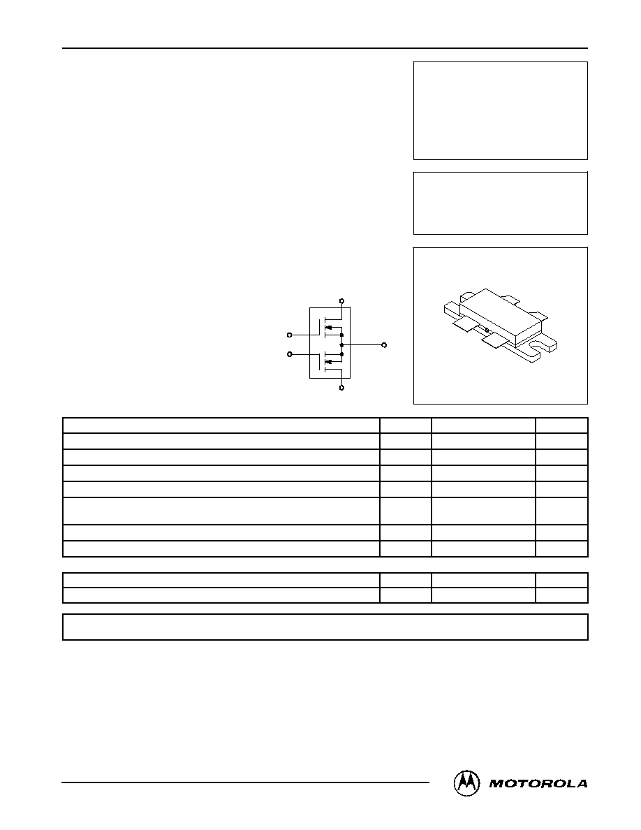
MRF141G
300 W, 28 V, 175 MHz
N¡CHANNEL
BROADBAND
RF POWER MOSFET
CASE 375¡04, STYLE 2
®
Motorola, Inc. 1997
D
G
S
(FLANGE)
D
G
REV 2

MRF141G
2
MOTOROLA RF DEVICE DATA
ELECTRICAL CHARACTERISTICS
(TC = 25
░
C unless otherwise noted)
Characteristic
Symbol
Min
Typ
Max
Unit
OFF CHARACTERISTICS (1)
Drain¡Source Breakdown Voltage
(VGS = 0, ID = 100 mA)
V(BR)DSS
65
--
--
Vdc
Zero Gate Voltage Drain Current
(VDS = 28 V, VGS = 0)
IDSS
--
--
5.0
mAdc
Gate¡Body Leakage Current
(VGS = 20 V, VDS = 0)
IGSS
--
--
1.0
Á
Adc
ON CHARACTERISTICS (1)
Gate Threshold Voltage
(VDS = 10 V, ID = 100 mA)
VGS(th)
1.0
3.0
5.0
Vdc
Drain¡Source On¡Voltage
(VGS = 10 V, ID = 10 A)
VDS(on)
0.1
0.9
1.5
Vdc
Forward Transconductance
(VDS = 10 V, ID = 5.0 A)
gfs
5.0
7.0
--
mhos
DYNAMIC CHARACTERISTICS (1)
Input Capacitance
(VDS = 28 V, VGS = 0, f = 1.0 MHz)
Ciss
--
350
--
pF
Output Capacitance
(VDS = 28 V, VGS = 0, f = 1.0 MHz)
Coss
--
420
--
pF
Reverse Transfer Capacitance
(VDS = 28 V, VGS = 0, f = 1.0 MHz)
Crss
--
35
--
pF
FUNCTIONAL TESTS (2)
Common Source Amplifier Power Gain
(VDD = 28 V, Pout = 300 W, IDQ = 500 mA, f = 175 MHz)
Gps
12
14
--
dB
Drain Efficiency
(VDD = 28 V, Pout = 300 W, f = 175 MHz, ID (Max) = 21.4 A)
45
55
--
%
Load Mismatch
(VDD = 28 V, Pout = 300 W, IDQ = 500 mA, f = 175 MHz,
VSWR 5:1 at all Phase Angles)
No Degradation in Output Power
NOTES:
1. Each side measured separately.
2. Measured in push¡pull configuration.
3
MRF141G
MOTOROLA RF DEVICE DATA
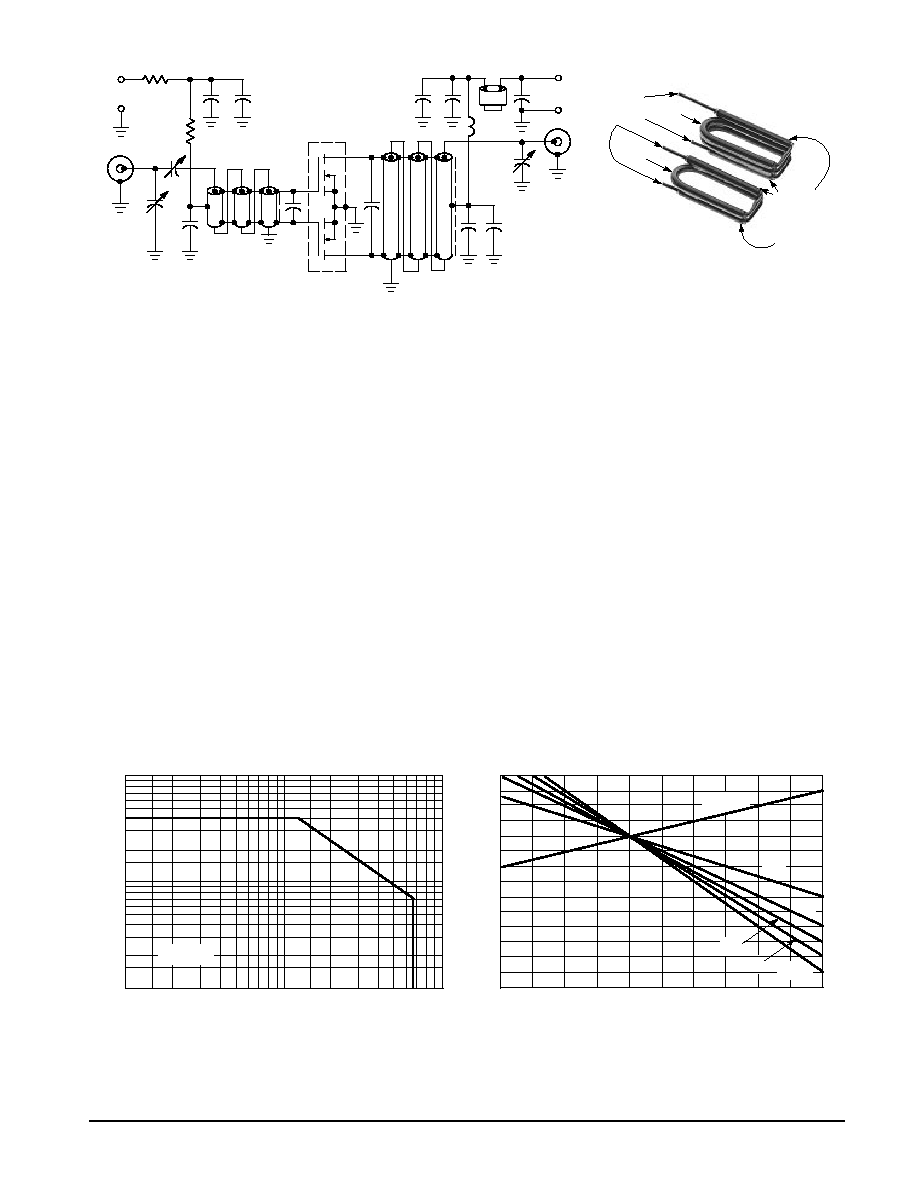
Figure 1. 175 MHz Test Circuit
C1 -- Arco 402, 1.5 ¡ 20 pF
C2 -- Arco 406, 15 ¡ 115 pF
C3, C4, C8, C9, C10 -- 1000 pF Chip
C5, C11 -- 0.1
Á
F Chip
C6 -- 330 pF Chip
C7 -- 200 pF and 180 pF Chips in Parallel
C12 -- 0.47
Á
F Ceramic Chip, Kemet 1215 or Equivalent
C13 -- Arco 403, 3.0 ¡ 35 pF
L1 -- 10 Turns AWG #16 Enameled Wire,
L1 --
Close Wound, 1/4
I.D.
L2 -- Ferrite Beads of Suitable Material for
L2 --
1.5 ¡ 2.0
Á
H Total Inductance
R1 -- 100 Ohms, 1/2 W
R2 -- 1.0 kOhm, 1/2 W
Unless Otherwise Noted, All Chip Capacitors are ATC Type 100 or Equivalent.
T1 -- 9:1 RF Transformer. Can be made of 15 ¡ 18 Ohms
T1 --
Semirigid Co¡Ax, 62 ¡ 90 Mils O.D.
T2 -- 1:9 RF Transformer. Can be made of 15 ¡ 18 Ohms
T2 --
Semirigid Co¡Ax, 70 ¡ 90 Mils O.D.
Board Material -- 0.062
Fiberglass (G10),
1 oz. Copper Clad, 2 Sides,
r = 5
NOTE: For stability, the input transformer T1 must be loaded
NOTE:
with ferrite toroids or beads to increase the common
NOTE:
mode inductance. For operation below 100 MHz. The
NOTE:
same is required for the output transformer.
See pictures for construction details.
Figure 2. DC Safe Operating Area
Figure 3. Gate¡Source Voltage versus
Case Temperature
TYPICAL CHARACTERISTICS
R1
C4
C5
+
¡
BIAS 0 ¡ 6 V
C2
INPUT
C1
C3
T1
C6
C7
T2
C8
C9
L1
C10
C11
L2
C12
+
¡
28 V
OUTPUT
C13
100
10
1
1
10
100
VDS, DRAIN¡TO¡SOURCE VOLTAGE (VOLTS)
I D
, DRAIN CURRENT
(AMPS)
TC = 25
░
C
V
GS
, GA
TE-SOURCE
VOL
T
AGE
(NORMALIZED)
1.04
¡ 25
TC, CASE TEMPERATURE (
░
C)
1.03
1.02
1.01
1
0.99
0.98
0.97
0.96
0.95
0.94
0.93
0.92
0.91
0.9
0
25
50
75
100
ID = 5 A
4 A
2 A
1 A
0.5 A
0.25 A
DUT
HIGH
IMPEDANCE
WINDINGS
CENTER
TAP
4:1
IMPEDANCE
RATIO
9:1
IMPEDANCE
RATIO
CONNECTIONS
TO LOW
IMPEDANCE
WINDINGS
CENTER
TAP

MRF141G
4
MOTOROLA RF DEVICE DATA
Figure 4. Common Source Unity Gain Frequency
versus Drain Current
Figure 5. Capacitance versus
Drain¡Source Voltage
Figure 6. Power Gain versus Frequency
TYPICAL CHARACTERISTICS
Figure 7. Output Power versus Supply Voltage
2000
0
ID, DRAIN CURRENT (AMPS)
2
4
6
8
10
12
14
16
18
20
0
10
20
5
15
25
1000
0
2000
200
20
VDS, DRAIN¡TO¡SOURCE VOLTAGE (VOLTS)
VDS = 20 V
10 V
NOTE: Data shown applies to each half of MRF141G.
f
,
UNITY
GAIN FREQUENCY
(MHz)
T
C, CAP
ACIT
ANCE
(pF)
NOTE: Data shown applies to each half of MRF141G.
Coss
Ciss
Crss
G
PS
, POWER GAIN (dB)
30
f, FREQUENCY (MHz)
2
25
20
15
10
5
5
10
30
100
200
VDD = 28 V
IDQ = 2 x 250 mA
Pout = 300 W
400
SUPPLY VOLTAGE (VOLTS)
12
P
, OUTPUT
POWER
(W
A
TTS)
out
350
300
250
200
150
100
50
0
14
16
18
20
22
24
26
28
Figure 8. Input and Output Impedances
f = 175 MHz
IDQ = 250 mA x 2
Pin = 30 W
20 W
10 W
Zo = 10
f = 175 MHz
INPUT, Zin
(GATE TO GATE)
30
100
150
125
30
f = 175 MHz
150
125
100
OUTPUT, ZOL*
(DRAIN TO DRAIN)
ZOL* = Conjugate of the optimum load impedance
ZOL* =
into which the device output operates at a
ZOL* =
given output power, voltage and frequency.
5
MRF141G
MOTOROLA RF DEVICE DATA
RF POWER MOSFET CONSIDERATIONS
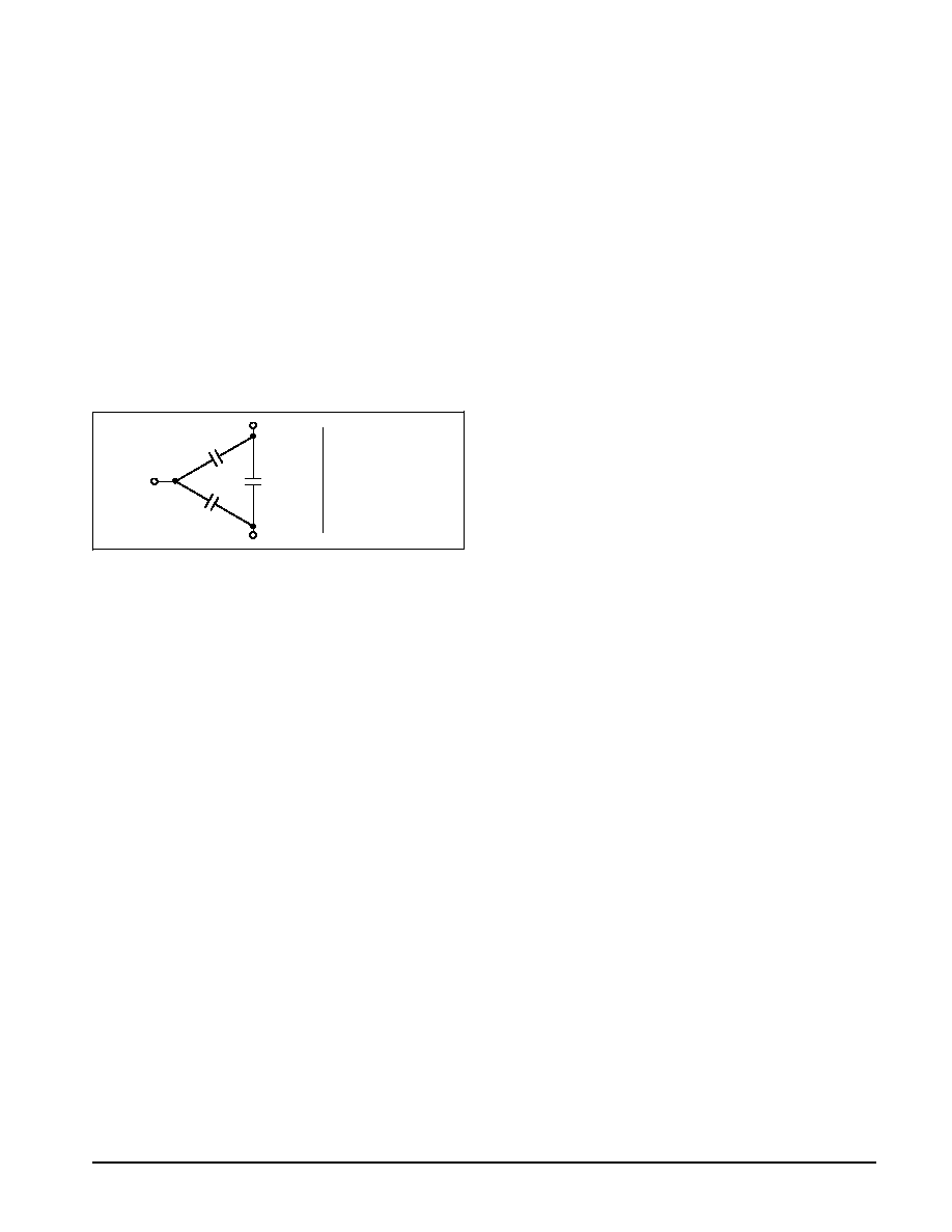
MOSFET CAPACITANCES
The physical structure of a MOSFET results in capacitors
between the terminals. The metal anode gate structure de-
termines the capacitors from gate¡to¡drain (Cgd), and gate¡
to¡source (Cgs). The PN junction formed during the
fabrication of the MOSFET results in a junction capacitance
from drain¡to¡source (Cds).
These capacitances are characterized as input (Ciss), out-
put (Coss) and reverse transfer (Crss) capacitances on data
sheets. The relationships between the inter¡terminal capaci-
tances and those given on data sheets are shown below. The
Ciss can be specified in two ways:
1. Drain shorted to source and positive voltage at the gate.
2. Positive voltage of the drain in respect to source and zero
volts at the gate. In the latter case the numbers are lower.
However, neither method represents the actual operat-
ing conditions in RF applications.
Cgd
GATE
SOURCE
Cgs
DRAIN
Cds
Ciss = Cgd = Cgs
Coss = Cgd = Cds
Crss = Cgd
LINEARITY AND GAIN CHARACTERISTICS
In addition to the typical IMD and power gain data pres-
ented, Figure 4 may give the designer additional information
on the capabilities of this device. The graph represents the
small signal unity current gain frequency at a given drain cur-
rent level. This is equivalent to fT for bipolar transistors.
Since this test is performed at a fast sweep speed, heating of
the device does not occur. Thus, in normal use, the higher
temperatures may degrade these characteristics to some ex-
tent.
DRAIN CHARACTERISTICS
One figure of merit for a FET is its static resistance in the
full¡on condition. This on¡resistance, VDS(on), occurs in the
linear region of the output characteristic and is specified un-
der specific test conditions for gate¡source voltage and drain
current. For MOSFETs, VDS(on) has a positive temperature
coefficient and constitutes an important design consideration
at high temperatures, because it contributes to the power
dissipation within the device.
GATE CHARACTERISTICS
The gate of the MOSFET is a polysilicon material, and is
electrically isolated from the source by a layer of oxide. The
input resistance is very high -- on the order of 109 ohms --
resulting in a leakage current of a few nanoamperes.
Gate control is achieved by applying a positive voltage
slightly in excess of the gate¡to¡source threshold voltage,
VGS(th).
Gate Voltage Rating -- Never exceed the gate voltage
rating. Exceeding the rated VGS can result in permanent
damage to the oxide layer in the gate region.
Gate Termination -- The gate of this device is essentially
capacitor. Circuits that leave the gate open¡circuited or float-
ing should be avoided. These conditions can result in turn¡
on of the device due to voltage build¡up on the input
capacitor due to leakage currents or pickup.
Gate Protection -- This device does not have an internal
monolithic zener diode from gate¡to¡source. If gate protec-
tion is required, an external zener diode is recommended.
Using a resistor to keep the gate¡to¡source impedance
low also helps damp transients and serves another important
function. Voltage transients on the drain can be coupled to
the gate through the parasitic gate¡drain capacitance. If the
gate¡to¡source impedance and the rate of voltage change
on the drain are both high, then the signal coupled to the gate
may be large enough to exceed the gate¡threshold voltage
and turn the device on.
HANDLING CONSIDERATIONS
When shipping, the devices should be transported only in
antistatic bags or conductive foam. Upon removal from the
packaging, careful handling procedures should be adhered
to. Those handling the devices should wear grounding straps
and devices not in the antistatic packaging should be kept in
metal tote bins. MOSFETs should be handled by the case
and not by the leads, and when testing the device, all leads
should make good electrical contact before voltage is ap-
plied. As a final note, when placing the FET into the system it
is designed for, soldering should be done with a grounded
iron.
DESIGN CONSIDERATIONS
The MRF141G is an RF Power, MOS, N¡channel en-
hancement mode field¡effect transistor (FET) designed for
HF and VHF power amplifier applications.
Motorola Application Note AN211A, FETs in Theory and
Practice, is suggested reading for those not familiar with the
construction and characteristics of FETs.
The major advantages of RF power MOSFETs include
high gain, low noise, simple bias systems, relative immunity
from thermal runaway, and the ability to withstand severely
mismatched loads without suffering damage. Power output
can be varied over a wide range with a low power dc control
signal.
DC BIAS
The MRF141G is an enhancement mode FET and, there-
fore, does not conduct when drain voltage is applied. Drain
current flows when a positive voltage is applied to the gate.
RF power FETs require forward bias for optimum perfor-
mance. The value of quiescent drain current (IDQ) is not criti-
cal for many applications. The MRF141G was characterized
at IDQ = 250 mA, each side, which is the suggested minimum
value of IDQ. For special applications such as linear amplifi-
cation, IDQ may have to be selected to optimize the critical
parameters.
The gate is a dc open circuit and draws no current. There-
fore, the gate bias circuit may be just a simple resistive divid-
er network. Some applications may require a more elaborate
bias sytem.
GAIN CONTROL
Power output of the MRF141G may be controlled from its
rated value down to zero (negative gain) by varying the dc
gate voltage. This feature facilitates the design of manual
gain control, AGC/ALC and modulation systems.