
1
Motorola Optoelectronics Device Data
Small Outline Optoisolators
Transistor Output (Low Input Current)
These devices consist of a gallium arsenide infrared emitting diode optically
coupled to a monolithic silicon phototransistor detector, in a surface mountable,
small outline, plastic package. They are ideally suited for high density
applications, and eliminate the need for throughÙtheÙboard mounting.
ñ
Convenient Plastic SOICÙ8 Surface Mountable Package Style
ñ
Low LED Input Current Required, for Easier Logic Interfacing
ñ
Standard SOICÙ8 Footprint, with 0.050
Lead Spacing
ñ
Shipped in Tape and Reel, which Conforms to EIA Standard RS481A
ñ
Compatible with Dual Wave, Vapor Phase and IR Reflow Soldering
ñ
High InputÙOutput Isolation of 3000 Vac (rms) Guaranteed
ñ
UL Recognized
File #E54915
Ordering Information:
ñ
To obtain MOC215, 216, 217 in Tape and Reel, add R2 suffix to device numbers:
R2 = 2500 units on 13
reel
ñ
To obtain MOC215, 216, 217 in quantities of 50 (shipped in sleeves) -- No Suffix
Marking Information:
ñ
MOC215 = 215
ñ
MOC216 = 216
ñ
MOC217 = 217
Applications:
ñ
Low power Logic Circuits
ñ
Interfacing and coupling systems of different potentials and impedances
ñ
Telecommunications equipment
ñ
Portable electronics
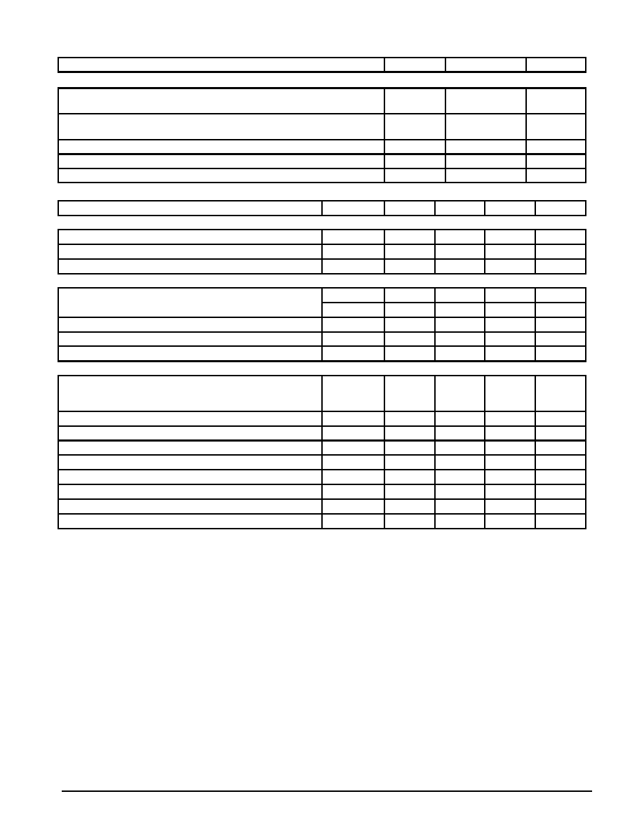
MAXIMUM RATINGS
(TA = 25
¯
C unless otherwise noted)
Rating
Symbol
Value
Unit
INPUT LED
Forward Current -- Continuous
IF
60
mA
Forward Current -- Peak (PW = 100
ç
s, 120 pps)
IF(pk)
1.0
A
Reverse Voltage
VR
6.0
V
LED Power Dissipation @ TA = 25
¯
C
Derate above 25
¯
C
PD
90
0.8
mW
mW/
¯
C
OUTPUT TRANSISTOR
CollectorÙEmitter Voltage
VCEO
30
V
CollectorÙBase Voltage
VCBO
70
V
EmitterÙCollector Voltage
VECO
7.0
V
Collector Current -- Continuous
IC
150
mA
Detector Power Dissipation @ TA = 25
¯
C
Derate above 25
¯
C
PD
150
1.76
mW
mW/
¯
C
NOTE: Thickness through insulation between input and output is
0.5 mm.
Preferred devices are Motorola recommended choices for future use and best overall value.
Order this document
by MOC215/D
MOTOROLA
SEMICONDUCTOR TECHNICAL DATA
ˋ
Motorola, Inc. 1995
MOC215
MOC216
MOC217
Motorola Preferred Devices
[CTR = 20% Min]
[CTR = 50% Min]
[CTR = 100% Min]
SMALL OUTLINE
OPTOISOLATORS
TRANSISTOR OUTPUT
CASE 846Ù01, STYLE 1
PLASTIC
SCHEMATIC
1. LED ANODE
2. LED CATHODE
3. NO CONNECTION
4. NO CONNECTION
5. EMITTER
6. COLLECTOR
7. BASE
8. NO CONNECTION
1
2
3
8
6
5
4
7
REV 1
MOC215 MOC216 MOC217
2
Motorola Optoelectronics Device Data
MAXIMUM RATINGS -- continued
(TA = 25
¯
C unless otherwise noted)
Rating
Symbol
Value
Unit
TOTAL DEVICE
InputÙOutput Isolation Voltage(1,2)
(60 Hz, 1.0 sec. duration)
VISO
3000
Vac(rms)
Total Device Power Dissipation @ TA = 25
¯
C
Derate above 25
¯
C
PD
250
2.94
mW
mW/
¯
C
Ambient Operating Temperature Range(3)
TA
Ù55 to +100
¯
C
Storage Temperature Range(3)
Tstg
Ù55 to +150
¯
C
Lead Soldering Temperature (1/16
from case, 10 sec. duration)
--
260
¯
C
ELECTRICAL CHARACTERISTICS
(TA = 25
¯
C unless otherwise noted)(4)
Characteristic
Symbol
Min
Typ(4)
Max
Unit
INPUT LED
Forward Voltage (IF = 1.0 mA)
VF
--
1.05
1.3
V
Reverse Leakage Current (VR = 6.0 V)
IR
--
0.1
100
m
A
Capacitance
C
--
18
--
pF
OUTPUT TRANSISTOR
CollectorÙEmitter Dark Current
(VCE = 5.0 V, TA = 25
¯
C)
ICEO1
--
1.0
50
nA
(VCE = 5.0 V, TA = 100
¯
C)
ICEO2
--
1.0
--
ç
A
CollectorÙEmitter Breakdown Voltage (IC = 100
ç
A)
V(BR)CEO
30
90
--
V
EmitterÙCollector Breakdown Voltage (IE = 100
ç
A)
V(BR)ECO
7.0
7.8
--
V
CollectorÙEmitter Capacitance (f = 1.0 MHz, VCE = 0)
CCE
--
7.0
--
pF
COUPLED
Output Collector Current
MOC215
(IF = 1.0 mA, VCE = 5.0 V)
MOC216
MOC217
IC (CTR)(5)
200 (20)
500 (50)
1.0 (100)
500(50)
800 (80)
1.3 (130)
--
--
--
ç
A (%)
ç
A (%)
mA (%)
CollectorÙEmitter Saturation Voltage (IC = 100
ç
A, IF = 1.0 mA)
VCE(sat)
--
0.35
0.4
V
TurnÙOn Time (IC = 2.0 mA, VCC = 10 V, RL = 100
)
ton
--
7.5
--
ç
s
TurnÙOff Time (IC = 2.0 mA, VCC = 10 V, RL = 100
)
toff
--
5.7
--
ç
s
Rise Time (IC = 2.0 mA, VCC = 10 V, RL = 100
)
tr
--
3.2
--
ç
s
Fall Time (IC = 2.0 mA, VCC = 10 V, RL = 100
)
tf
--
4.7
--
ç
s
InputÙOutput Isolation Voltage (f = 60 Hz, t = 1.0 sec.)(1,2)
VISO
3000
--
--
Vac(rms)
Isolation Resistance (VIÙO = 500 V)(2)
RISO
1011
--
--
Isolation Capacitance (VIÙO = 0, f = 1.0 MHz)(2)
CISO
--
0.2
--
pF
1. InputÙOutput Isolation Voltage, VISO, is an internal device dielectric breakdown rating.
2. For this test, pins 1 and 2 are common, and pins 5, 6 and 7 are common.
3. Refer to Quality and Reliability Section in Opto Data Book for information on test conditions.
4. Always design to the specified minimum/maximum electrical limits (where applicable).
5. Current Transfer Ratio (CTR) = IC/IF x 100%.
MOC215 MOC216 MOC217
3
Motorola Optoelectronics Device Data
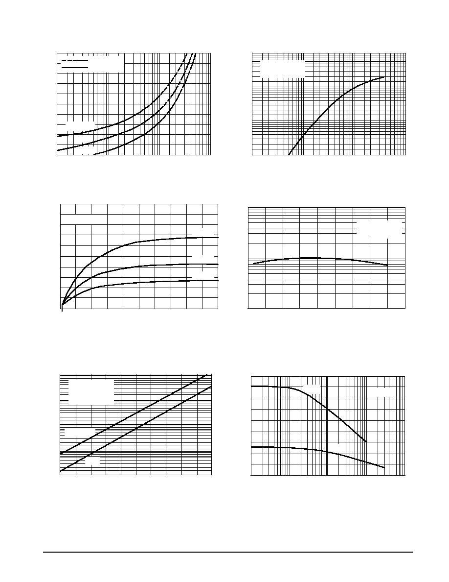
C
IF, LED INPUT CURRENT (mA)
5
2
1
0.5
0.2
0.1
0.05
0.1
1
10
Figure 1. LED Forward Voltage versus Forward Current
IF, LED FORWARD CURRENT (mA)
10
1
2
0.001
1000
100
1
1.2
1.4
1.6
1.8
Figure 2. Output Current versus Input Current
V
F
, FOR
W
ARD VOL
T
AGE (VOL
TS)
I
, OUTPUT
COLLECT
OR CURRENT
(NORMALIZED)
PULSE ONLY
PULSE OR DC
TYPICAL CHARACTERISTICS
NORMALIZED TO:
IF = 1 mA
TA = Ù 55
¯
C
25
¯
C
100
¯
C
100
10
1
0.1
0.01
20
TA, AMBIENT TEMPERATURE (
¯
C)
120
100
80
60
40
20
0
Ù20
Ù40
Ù60
0.1
1
10
Figure 3. Output Current versus
CollectorÙEmitter Voltage
18
16
14
12
10
8
6
4
V, VOLTAGE (VOLTS)
2
I C
, OUTPUT
COLLECT
OR CURRENT
(NORMALIZED)
C, CAP
ACIT
ANCE (pF)
1
10
100
0.1
0
20
40
60
80
100
TA, AMBIENT TEMPERATURE (
¯
C)
I CEO
, COLLECT
ORÙEMITTER DARK CURRENT
(NORMALIZED)
Figure 4. Output Current versus
Ambient Temperature
Figure 5. Dark Current versus Ambient Temperature
Figure 6. Capacitance versus Voltage
2
1.8
1.6
1.4
1.2
1
0.8
0.6
0
VCE, COLLECTORÙEMITTER VOLTAGE (VOLTS)
10
9
8
0
1
2
3
4
5
6
7
0.4
0.2
I C
, OUTPUT
COLLECT
OR CURRENT
(mA)
NORMALIZED TO:
TA = 25
¯
C
IF = 1 mA
MOC216
MOC215
MOC217
NORMALIZED TO:
VCE = 10 V
TA = 25
¯
C
VCE = 30 V
10 V
CLED
CCE
f = 1 MHz
MOC215 MOC216 MOC217
4
Motorola Optoelectronics Device Data
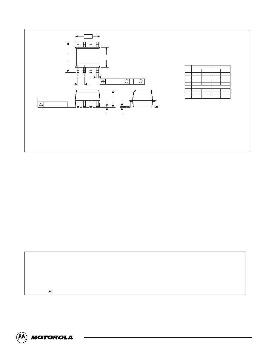
PACKAGE DIMENSIONS
STYLE 1:
PIN 1. ANODE
2. CATHODE
3. NC
4. NC
5. EMITTER
6. COLLECTOR
7. BASE
8. NC
DIM
A
MIN
MAX
MIN
MAX
MILLIMETERS
0.182
0.202
4.63
5.13
INCHES
B
0.144
0.164
3.66
4.16
C
0.123
0.143
3.13
3.63
D
0.011
0.021
0.28
0.53
G
0.050 BSC
1.27 BSC
H
0.003
0.008
0.08
0.20
J
0.006
0.010
0.16
0.25
K
0.224
0.244
5.69
6.19
NOTES:
1. DIMENSIONING AND TOLERANCING PER ANSI
Y14.5M, 1982.
2. CONTROLLING DIMENSION: INCH.
B
K
D
G
8 PL
0.13 (0.005)
M
T A
M
J
H
C
SEATING
PLANE
0.038 (0.0015)
CASE 846Ù01
1
8
5
4
ÙAÙ
ÙTÙ
ISSUE B
Motorola reserves the right to make changes without further notice to any products herein. Motorola makes no warranty, representation or guarantee regarding
the suitability of its products for any particular purpose, nor does Motorola assume any liability arising out of the application or use of any product or circuit,
and specifically disclaims any and all liability, including without limitation consequential or incidental damages. "Typical" parameters can and do vary in different
applications. All operating parameters, including "Typicals" must be validated for each customer application by customer's technical experts. Motorola does
not convey any license under its patent rights nor the rights of others. Motorola products are not designed, intended, or authorized for use as components in
systems intended for surgical implant into the body, or other applications intended to support or sustain life, or for any other application in which the failure of
the Motorola product could create a situation where personal injury or death may occur. Should Buyer purchase or use Motorola products for any such
unintended or unauthorized application, Buyer shall indemnify and hold Motorola and its officers, employees, subsidiaries, affiliates, and distributors harmless
against all claims, costs, damages, and expenses, and reasonable attorney fees arising out of, directly or indirectly, any claim of personal injury or death
associated with such unintended or unauthorized use, even if such claim alleges that Motorola was negligent regarding the design or manufacture of the part.
Motorola and
are registered trademarks of Motorola, Inc. Motorola, Inc. is an Equal Opportunity/Affirmative Action Employer.
How to reach us:
USA / EUROPE: Motorola Literature Distribution;
JAPAN: Nippon Motorola Ltd.; TatsumiÙSPDÙJLDC, Toshikatsu Otsuki,
P.O. Box 20912; Phoenix, Arizona 85036. 1Ù800Ù441Ù2447
6F SeibuÙButsuryuÙCenter, 3Ù14Ù2 Tatsumi KotoÙKu, Tokyo 135, Japan. 03Ù3521Ù8315
MFAX: RMFAX0@email.sps.mot.com Ù TOUCHTONE (602) 244Ù6609
HONG KONG: Motorola Semiconductors H.K. Ltd.; 8B Tai Ping Industrial Park,
INTERNET: http://DesignÙNET.com
51 Ting Kok Road, Tai Po, N.T., Hong Kong. 852Ù26629298
MOC215/D
*MOC215/D*