MOTOROLA
SEMICONDUCTOR
TECHNICAL DATA
Motorola TVS/Zener Device Data
7-1
500 mW Leadless (SOD-123) Data Sheet
Designer's
TM
Data Sheet
Surface Mount Silicon Zener Diodes
Plastic SOD 123 Package
Three complete series of Zener Diodes are offered in the convenient, surface mount
plastic SOD-123 package. These devices provide a convenient alternative to the leadless
34 package style.
À
500 mW Rating on FR-4 or FR-5 Board
À
Package Designed for Optimal Automated Board Assembly
À
Corrosion Resistant Finish, Easily Solderable
À
ESD Rating of Class 3 (exceeding 16 kV) per the Human Body Model
À
Small Package Size for High Density Applications
À
Available in 8 mm Tape and Reel
Add "T1" to the device number to order the 7 inch / 3000 unit reel.
Add "T3" to the device number to order the 13 inch / 10,000 unit reel.
À
Wafer Fab Location: Phoenix, Arizona
Assembly/Test Location: Seremban, Malaysia
MMSZ2V4T1 thru MMSZ75T1
À
Specified Similar to European BZV55C Series
À
Wide Voltage Range -- 2.4 to 75 Volts
DEVICE RATING
(TA = 25
░
C unless otherwise noted)
Rating
Symbol
Value
Unit
Power Dissipation on FR-4 or FR-5 Board [1]
Derate above TL = 75
░
C
PD
--
500
6.7
mW
mW/
░
C
Thermal Resistance Junction to Lead [2]
Thermal Resistance Junction to Ambient [2]
R
JL
R
JA
150
340
░
C/W
Junction Temperature Range
TJ
¡55 to +150
░
C
Storage Temperature Range
Tstg
¡55 to +150
░
C
Lead Solder Temperature ¡ Maximum (10 sec. duration)
--
260
░
C
[1] FR-4 or FR-5 = 3.5 x 1.5 inches, using the Motorola minimum recommended footprint as shown in Figure 11.
[2] Thermal Resistance measurement obtained via Infrared Scan Method
Designer's Data for "Worst Case'' Conditions -- The Designer's Data Sheet permits the design of most circuits entirely from the information presented. Limit curves -- representing
boundaries on device characteristics -- are given to facilitate "worst case'' design.
Designer's is a trademark of Motorola, Inc.
Thermal Clad is a trademark of the Bergquist Company.
Preferred devices are Motorola recommended choices for future use and best overall value.
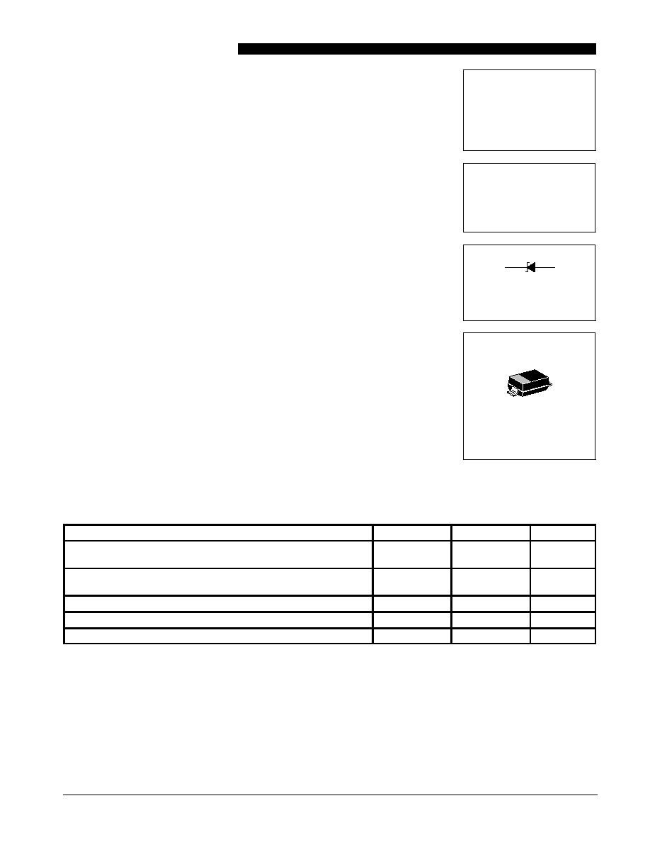
MMSZ2V4T1
SERIES
PLASTIC SURFACE
MOUNT
ZENER DIODES
500 MILLIWATTS
1.8 ¡ 91 VOLTS
CASE 425, STYLE 1
PLASTIC
1: CATHODE
2: ANODE
1
2

MMSZ2V4T1 Series
Motorola TVS/Zener Device Data
7-2
500 mW Leadless (SOD-123) Data Sheet
ELECTRICAL CHARACTERISTICS
(TA = 25
░
C unless otherwise noted), (VF = 0.9 V Max. @ IF = 10 mA for all types)
T
M
ki
Zener Voltage
VZ1 (Volts)
@ IZT1 = 5 mA
[1][2]
Max Zener
Impedance
ZZT1
@ IZT1 = 5 mA
Max
Reverse
Leakage
Current
Zener Voltage
VZ2 (Volts)
@ IZT2 = 1 mA
[1]
Max Zener
Impedance
ZZT2
@ IZT1 = 1 mA
Type
Number
Marking
Nom
Min
Max
@ IZT1 = 5 mA
[3]
IR @ VR
Á
A Volts
Min
Max
@ IZT1 = 1 mA
[3]
MMSZ2V4T1
T1
2.4
2.28
2.52
100
50
1
1.7
2.1
600
MMSZ2V7T1
T2
2.7
2.57
2.84
100
20
1
1.9
2.4
600
MMSZ3V0T1
T3
3.0
2.85
3.15
95
10
1
2.1
2.7
600
MMSZ3V3T1
T4
3.3
3.14
3.47
95
5
1
2.3
2.9
600
MMSZ3V6T1
T5
3.6
3.42
3.78
90
5
1
2.7
3.3
600
MMSZ3V9T1
U1
3.9
3.71
4.10
90
3
1
2.9
3.5
600
MMSZ4V3T1
U2
4.3
4.09
4.52
90
3
1
3.3
4.0
600
MMSZ4V7T1
U3
4.7
4.47
4.94
80
3
2
3.7
4.7
500
MMSZ5V1T1
U4
5.1
4.85
5.36
60
2
2
4.2
5.3
480
MMSZ5V6T1
U5
5.6
5.32
5.88
40
1
2
4.8
6.0
400
MMSZ6V2T1
V1
6.2
5.89
6.51
10
3
4
5.6
6.6
150
MMSZ6V8T1
V2
6.8
6.46
7.14
15
2
4
6.3
7.2
80
MMSZ7V5T1
V3
7.5
7.13
7.88
15
1
5
6.9
7.9
80
MMSZ8V2T1
V4
8.2
7.79
8.61
15
0.7
5
7.6
8.7
80
MMSZ9V1T1
V5
9.1
8.65
9.56
15
0.5
6
8.4
9.6
100
MMSZ10T1
A1
10
9.50
10.50
20
0.2
7
9.3
10.6
150
MMSZ11T1
A2
11
10.45
11.55
20
0.1
8
10.2
11.6
150
MMSZ12T1
A3
12
11.40
12.60
25
0.1
8
11.2
12.7
150
MMSZ13T1
A4
13
12.35
13.65
30
0.1
8
12.3
14.0
170
MMSZ15T1
A5
15
14.25
15.75
30
0.05
10.5
13.7
15.5
200
MMSZ16T1
X1
16
15.20
16.80
40
0.05
11.2
15.2
17.0
200
MMSZ18T1
X2
18
17.10
18.90
45
0.05
12.6
16.7
19.0
225
MMSZ20T1
X3
20
19.00
21.00
55
0.05
14
18.7
21.1
225
MMSZ22T1
X4
22
20.80
23.10
55
0.05
15.4
20.7
23.2
250
MMSZ24T1
X5
24
22.80
25.20
70
0.05
16.8
22.7
25.5
250
MMSZ27T1
Y1
27
25.65
28.35
80
0.05
18.9
25
28.9
300
MMSZ30T1
Y2
30
28.50
31.50
80
0.05
21
27.8
32
300
MMSZ33T1
Y3
33
31.35
34.65
80
0.05
23.1
30.8
35
325
MMSZ36T1
Y4
36
34.20
37.80
90
0.05
25.2
33.8
38
350
MMSZ39T1
Y5
39
37.05
40.95
130
0.05
27.3
36.7
41
350
MMSZ43T1
Z1
43
40.85
45.15
150
0.05
30.1
39.7
46
375
MMSZ47T1
Z2
47
44.65
49.35
170
0.05
32.9
43.7
50
375
MMSZ51T1
Z3
51
48.45
53.55
180
0.05
35.7
47.6
54
400
MMSZ56T1
Z4
56
53.20
58.80
200
0.05
39.2
51.5
60
425
MMSZ62T1
Z5
62
58.90
65.10
215
0.05
43.4
57.4
66
450
MMSZ68T1
Z6
68
64.60
71.40
240
0.05
47.6
63.4
72
475
MMSZ75T1
Z7
75
71.25
78.75
255
0.05
52.5
69.4
79
500
[1] Zener voltage is measured with the zener current applied for PW = 1.0 ms.
[2] All part numbers shown indicate a V
Z tolerance of
▒
5%.
[3] Z
ZT1 and ZZT2 are measured by dividing the AC voltage drop across the device by the AC current applied. The specified limits are for IZ(AC) = 0.1 IZ(DC),
[3]
with the AC frequency = 1 kHz.
[4] The zener impedance, Z
ZT2, for the 27 through 75 volt types is tested at 0.5 mA rather than the test current of 0.1 mA used for VZ2.

MMSZ2V4T1 Series
Motorola TVS/Zener Device Data
7-3
500 mW Leadless (SOD-123) Data Sheet
TYPICAL CHARACTERISTICS
VZ
, TEMPERA
TURE COEFFICIENT
(mV/
C)
░
VZ, NOMINAL ZENER VOLTAGE (V)
¡ 3
¡ 2
¡1
0
1
2
3
4
5
6
7
8
12
11
10
9
8
7
6
5
4
3
2
Figure 1. Temperature Coefficients
(Temperature Range ¡ 55
░
C to +150
░
C)
TYPICAL TC VALUES
FOR MMSZ5221BT1 SERIES
VZ @ IZT
VZ
, TEMPERA
TURE COEFFICIENT
(mV/
C)
░
100
10
1
10
100
VZ, NOMINAL ZENER VOLTAGE (V)
Figure 2. Temperature Coefficients
(Temperature Range ¡ 55
░
C to +150
░
C)
VZ @ IZT
P
D
, POWER DISSIP
A
TION (W
A
TTS)
1.2
1.0
0.8
0.6
0.4
0.2
0
150
125
100
75
50
25
0
T, TEMPERATURE (
░
C)
Figure 3. Steady State Power Derating
PD versus TA
PD versus TL
P
pk
, PEAK SURGE POWER (W
A
TTS)
0.1
PW, PULSE WIDTH (ms)
Figure 4. Maximum Nonrepetitive Surge Power
1
10
100
1000
1000
100
10
1
RECTANGULAR
WAVEFORM, TA = 25
░
C
100
VZ, NOMINAL ZENER VOLTAGE
Figure 5. Effect of Zener Voltage on
Zener Impedance
10
1
Z
ZT
, DYNAMIC IMPEDANCE (
)
1000
100
10
1
TJ = 25
░
C
IZ(AC) = 0.1 IZ(DC)
f = 1 kHz
IZ = 1 mA
5 mA
20 mA
VF, FORWARD VOLTAGE (V)
Figure 6. Typical Forward Voltage
1.2
1.1
1.0
0.9
0.8
0.7
0.6
0.5
0.4
I F
, FOR
W
ARD
CURRENT
(mA)
1000
100
10
1
75 V (MMSZ5267BT1)
91 V (MMSZ5270BT1)
150
░
C
75
░
C 25
░
C
0
░
C
TYPICAL TC VALUES
FOR MMSZ5221BT1 SERIES

MMSZ2V4T1 Series
Motorola TVS/Zener Device Data
7-4
500 mW Leadless (SOD-123) Data Sheet
TYPICAL CHARACTERISTICS
C, CAP
ACIT
ANCE
(pF)
100
VZ, NOMINAL ZENER VOLTAGE (V)
Figure 7. Typical Capacitance
1000
100
10
1
10
1
BIAS AT
50% OF VZ NOM
TA = 25
░
C
0 V BIAS
1 V BIAS
12
VZ, ZENER VOLTAGE (V)
Figure 9. Zener Voltage versus Zener Current
(VZ Up to 12 V)
100
10
1
0.1
0.01
10
8
6
4
2
0
TA = 25
░
C
I Z
, ZENER CURRENT
(mA)
VZ, ZENER VOLTAGE (V)
Figure 10. Zener Voltage versus Zener Current
(12 V to 91 V)
100
10
1
0.1
0.01
10
30
50
70
90
TA = 25
░
C
I R
, LEAKAGE CURRENT
(
A
)
Á
90
VZ, NOMINAL ZENER VOLTAGE (V)
Figure 8. Typical Leakage Current
1000
100
10
1
0.1
0.01
0.001
0.0001
0.00001
80
70
60
50
40
30
20
10
0
+150
░
C
+ 25
░
C
¡ 55
░
C
I Z
, ZENER CURRENT
(mA)
MMSZ2V4T1 Series
Motorola TVS/Zener Device Data
7-5
500 mW Leadless (SOD-123) Data Sheet
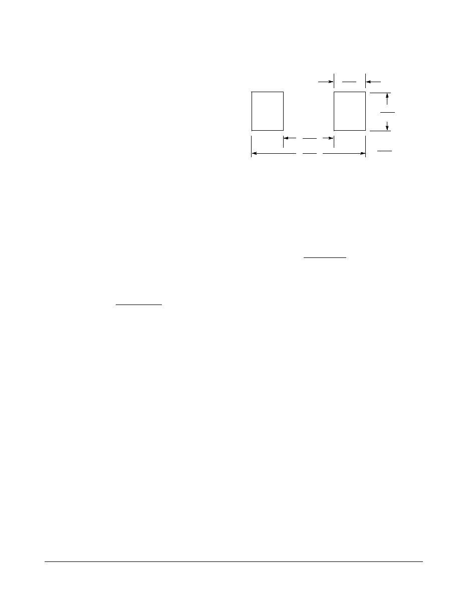
INFORMATION FOR USING THE SOD-123 SURFACE MOUNT PACKAGE
MINIMUM RECOMMENDED FOOTPRINTS FOR
SURFACE MOUNT APPLICATIONS
Surface mount board layout is a critical portion of the total
design. The footprint for the semiconductor packages must be
the correct size to ensure proper solder connection interface
between the board and the package.
The minimum recommended footprint for the SOD-123 is
shown at the right.
The SOD-123 package can be used on existing surface
mount boards which have been designed for the leadless 34
package style. The footprint compatibility makes conversion
from leadless 34 to SOD-123 straightforward.
╔╔╔╔
╔╔╔╔
╔╔╔╔
╔╔╔╔
╔╔╔╔
mm
inches
0.91
0.036
1.22
0.048
2.36
0.093
4.19
0.165
Figure 11. Minimum Recommended Footprint
SOD-123 POWER DISSIPATION
The power dissipation of the SOD-123 is a function of the
pad size. This can vary from the minimum pad size for
soldering to a pad size given for maximum power dissipation.
Power dissipation for a surface mount device is determined by
TJ(max), the maximum rated junction temperature of the die,
R
JA, the thermal resistance from the device junction to
ambient; and the operating temperature, TA. Using the values
provided on the data sheet for the SOD-123 package, PD can
be calculated as follows:
PD =
TJ(max) ¡ TA
R
JA
The values for the equation are found in the maximum
ratings table on the data sheet. Substituting these values into
the equation for an ambient temperature TA of 25
░
C, one can
calculate the power dissipation of the device which in this case
is 0.37 watts.
PD =
150
░
C ¡ 25
░
C
340
░
C/W
= 0.37 watts
The 340
░
C/W for the SOD-123 package assumes using
recommended footprint shown on FR-4 glass epoxy printed
circuit board. Another alternative is to use a ceramic substrate
or an aluminum core board such as Thermal Clad
TM
. By using
an aluminum core board material such as Thermal Clad, the
power dissipation can be doubled using the same footprint.
GENERAL SOLDERING PRECAUTIONS
The melting temperature of solder is higher than the rated
temperature of the device. When the entire device is heated
to a high temperature, failure to complete soldering within a
short time could result in device failure. Therefore, the
following items should always be observed in order to
minimize the thermal stress to which the devices are
subjected.
À
Always preheat the device.
À
The delta temperature between the preheat and soldering
should be 100
░
C or less.*
À
When preheating and soldering, the temperature of the
leads and the case must not exceed the maximum
temperature ratings as shown on the data sheet. When
using infrared heating with the reflow soldering method,
the difference shall be a maximum of 10
░
C.
À
The soldering temperature and time shall not exceed
260
░
C for more than 10 seconds.
À
When shifting from preheating to soldering, the maximum
temperature gradient shall be 5
░
C or less.
À
After soldering has been completed, the device should be
allowed to cool naturally for at least three minutes.
Gradual cooling should be used as the use of forced
cooling will increase the temperature gradient and result
in latent failure due to mechanical stress.
À
Mechanical stress or shock should not be applied during
cooling
* Soldering a device without preheating can cause excessive
thermal shock and stress which can result in damage to the
device.