Äîêóìåíòàöèÿ è îïèñàíèÿ www.docs.chipfind.ru
MOTOROLA
SEMICONDUCTOR TECHNICAL DATA
31
REV 6
©
Motorola, Inc. 1995
10/95
Octal 3-State
Noninverting D Flip-Flop
HighPerformance SiliconGate CMOS
The MC54/74HC374A is identical in pinout to the LS374. The device
inputs are compatible with standard CMOS outputs; with pullup resistors,
they are compatible with LSTTL outputs.
Data meeting the setup time is clocked to the outputs with the rising edge
of the clock. The Output Enable input does not affect the states of the
flipflops, but when Output Enable is high, the outputs are forced to the
highimpedance state; thus, data may be stored even when the outputs are
not enabled.
The HC374A is identical in function to the HC574A which has the input
pins on the opposite side of the package from the output. This device is
similar in function to the HC534A which has inverting outputs.
·
Output Drive Capability: 15 LSTTL Loads
·
Outputs Directly Interface to CMOS, NMOS, and TTL
·
Operating Voltage Range: 2.0 to 6.0 V
·
Low Input Current: 1.0
µ
A
·
High Noise Immunity Characteristic of CMOS Devices
·
In Compliance with the Requirements Defined by JEDEC Standard
No. 7A
·
Chip Complexity: 266 FETs or 66.5 Equivalent Gates
LOGIC DIAGRAM
DATA
INPUTS
D0
11
CLOCK
D1
D2
D3
D4
D5
D6
D7
18
17
14
13
8
7
4
3
1
OUTPUT ENABLE
19
Q0
Q1
Q2
Q3
Q4
Q5
Q6
Q7
16
15
12
9
6
5
2
PIN 20 = VCC
PIN 10 = GND
NONINVERTING
OUTPUTS
FUNCTION TABLE
Inputs
Output
Output
Enable
Clock
D
Q
L
H
H
L
L
L
L
L,H,
X
No Change
H
X
X
Z
X = don't care
Z = high impedance
MC54/74HC374A
PIN ASSIGNMENT
Q2
D1
D0
Q0
OUTPUT
ENABLE
GND
Q3
D3
D2
Q1
5
4
3
2
1
10
9
8
7
6
14
15
16
17
18
19
20
11
12
13
Q6
D6
D7
Q7
VCC
CLOCK
Q4
D4
D5
Q5
DW SUFFIX
SOIC PACKAGE
CASE 751D04
N SUFFIX
PLASTIC PACKAGE
CASE 73803
ORDERING INFORMATION
MC54HCXXXAJ
MC74HCXXXAN
MC74HCXXXADW
MC74HCXXXASD
MC74HCXXXADT
Ceramic
Plastic
SOIC
SSOP
TSSOP
DT SUFFIX
TSSOP PACKAGE
CASE 948E02
J SUFFIX
CERAMIC PACKAGE
CASE 73203
1
20
1
20
SD SUFFIX
SSOP PACKAGE
CASE 940C03
1
20
1
20
1
20
MC54/74HC374A
MOTOROLA
HighSpeed CMOS Logic Data
DL129 -- Rev 6
32
ÎÎÎÎÎÎÎÎÎÎÎÎÎÎÎÎÎÎÎÎÎÎÎ
ÎÎÎÎÎÎÎÎÎÎÎÎÎÎÎÎÎÎÎÎÎÎÎ
ÎÎÎÎÎÎÎÎÎÎÎÎÎÎÎÎÎÎÎÎÎÎÎ
ÎÎÎÎÎÎÎÎÎÎÎÎÎÎÎÎÎÎÎÎÎÎÎ
MAXIMUM RATINGS*
ÎÎÎ
ÎÎÎ
ÎÎÎ
ÎÎÎ
Symbol
ÎÎÎÎÎÎÎÎÎÎÎÎÎÎ
ÎÎÎÎÎÎÎÎÎÎÎÎÎÎ
ÎÎÎÎÎÎÎÎÎÎÎÎÎÎ
ÎÎÎÎÎÎÎÎÎÎÎÎÎÎ
Parameter
ÎÎÎÎÎÎ
ÎÎÎÎÎÎ
ÎÎÎÎÎÎ
ÎÎÎÎÎÎ
Value
ÎÎÎ
ÎÎÎ
ÎÎÎ
ÎÎÎ
Unit
ÎÎÎ
ÎÎÎ
ÎÎÎ
ÎÎÎ
VCC
ÎÎÎÎÎÎÎÎÎÎÎÎÎÎ
ÎÎÎÎÎÎÎÎÎÎÎÎÎÎ
ÎÎÎÎÎÎÎÎÎÎÎÎÎÎ
ÎÎÎÎÎÎÎÎÎÎÎÎÎÎ
DC Supply Voltage (Referenced to GND)
ÎÎÎÎÎÎ
ÎÎÎÎÎÎ
ÎÎÎÎÎÎ
ÎÎÎÎÎÎ
0.5 to + 7.0
ÎÎÎ
ÎÎÎ
ÎÎÎ
ÎÎÎ
V
ÎÎÎ
ÎÎÎ
ÎÎÎ
ÎÎÎ
Vin
ÎÎÎÎÎÎÎÎÎÎÎÎÎÎ
ÎÎÎÎÎÎÎÎÎÎÎÎÎÎ
ÎÎÎÎÎÎÎÎÎÎÎÎÎÎ
ÎÎÎÎÎÎÎÎÎÎÎÎÎÎ
DC Input Voltage (Referenced to GND)
ÎÎÎÎÎÎ
ÎÎÎÎÎÎ
ÎÎÎÎÎÎ
ÎÎÎÎÎÎ
1.5 to VCC + 1.5
ÎÎÎ
ÎÎÎ
ÎÎÎ
ÎÎÎ
V
ÎÎÎ
ÎÎÎ
ÎÎÎ
ÎÎÎ
Vout
ÎÎÎÎÎÎÎÎÎÎÎÎÎÎ
ÎÎÎÎÎÎÎÎÎÎÎÎÎÎ
ÎÎÎÎÎÎÎÎÎÎÎÎÎÎ
ÎÎÎÎÎÎÎÎÎÎÎÎÎÎ
DC Output Voltage (Referenced to GND)
ÎÎÎÎÎÎ
ÎÎÎÎÎÎ
ÎÎÎÎÎÎ
ÎÎÎÎÎÎ
0.5 to VCC + 0.5
ÎÎÎ
ÎÎÎ
ÎÎÎ
ÎÎÎ
V
ÎÎÎ
ÎÎÎ
ÎÎÎ
ÎÎÎ
Iin
ÎÎÎÎÎÎÎÎÎÎÎÎÎÎ
ÎÎÎÎÎÎÎÎÎÎÎÎÎÎ
ÎÎÎÎÎÎÎÎÎÎÎÎÎÎ
ÎÎÎÎÎÎÎÎÎÎÎÎÎÎ
DC Input Current, per Pin
ÎÎÎÎÎÎ
ÎÎÎÎÎÎ
ÎÎÎÎÎÎ
ÎÎÎÎÎÎ
±
20
ÎÎÎ
ÎÎÎ
ÎÎÎ
ÎÎÎ
mA
ÎÎÎ
ÎÎÎ
ÎÎÎ
ÎÎÎ
Iout
ÎÎÎÎÎÎÎÎÎÎÎÎÎÎ
ÎÎÎÎÎÎÎÎÎÎÎÎÎÎ
ÎÎÎÎÎÎÎÎÎÎÎÎÎÎ
ÎÎÎÎÎÎÎÎÎÎÎÎÎÎ
DC Output Current, per Pin
ÎÎÎÎÎÎ
ÎÎÎÎÎÎ
ÎÎÎÎÎÎ
ÎÎÎÎÎÎ
±
35
ÎÎÎ
ÎÎÎ
ÎÎÎ
ÎÎÎ
mA
ÎÎÎ
ÎÎÎ
ÎÎÎ
ÎÎÎ
ICC
ÎÎÎÎÎÎÎÎÎÎÎÎÎÎ
ÎÎÎÎÎÎÎÎÎÎÎÎÎÎ
ÎÎÎÎÎÎÎÎÎÎÎÎÎÎ
ÎÎÎÎÎÎÎÎÎÎÎÎÎÎ
DC Supply Current, VCC and GND Pins
ÎÎÎÎÎÎ
ÎÎÎÎÎÎ
ÎÎÎÎÎÎ
ÎÎÎÎÎÎ
±
75
ÎÎÎ
ÎÎÎ
ÎÎÎ
ÎÎÎ
mA
ÎÎÎ
ÎÎÎ
ÎÎÎ
ÎÎÎ
ÎÎÎ
PD
ÎÎÎÎÎÎÎÎÎÎÎÎÎÎ
ÎÎÎÎÎÎÎÎÎÎÎÎÎÎ
ÎÎÎÎÎÎÎÎÎÎÎÎÎÎ
ÎÎÎÎÎÎÎÎÎÎÎÎÎÎ
ÎÎÎÎÎÎÎÎÎÎÎÎÎÎ
Power Dissipation in Still Air, Plastic or Ceramic DIP
SOIC Package
SSOP or TSSOP Package
ÎÎÎÎÎÎ
ÎÎÎÎÎÎ
ÎÎÎÎÎÎ
ÎÎÎÎÎÎ
ÎÎÎÎÎÎ
750
500
450
ÎÎÎ
ÎÎÎ
ÎÎÎ
ÎÎÎ
ÎÎÎ
mW
ÎÎÎ
ÎÎÎ
ÎÎÎ
ÎÎÎ
Tstg
ÎÎÎÎÎÎÎÎÎÎÎÎÎÎ
ÎÎÎÎÎÎÎÎÎÎÎÎÎÎ
ÎÎÎÎÎÎÎÎÎÎÎÎÎÎ
ÎÎÎÎÎÎÎÎÎÎÎÎÎÎ
Storage Temperature
ÎÎÎÎÎÎ
ÎÎÎÎÎÎ
ÎÎÎÎÎÎ
ÎÎÎÎÎÎ
65 to + 150
ÎÎÎ
ÎÎÎ
ÎÎÎ
ÎÎÎ
_
C
ÎÎÎ
ÎÎÎ
ÎÎÎ
ÎÎÎ
ÎÎÎ
ÎÎÎ
TL
ÎÎÎÎÎÎÎÎÎÎÎÎÎÎ
ÎÎÎÎÎÎÎÎÎÎÎÎÎÎ
ÎÎÎÎÎÎÎÎÎÎÎÎÎÎ
ÎÎÎÎÎÎÎÎÎÎÎÎÎÎ
ÎÎÎÎÎÎÎÎÎÎÎÎÎÎ
ÎÎÎÎÎÎÎÎÎÎÎÎÎÎ
Lead Temperature, 1 mm from Case for 10 Seconds
(Plastic DIP, SOIC, SSOP or TSSOP Package)
(Ceramic DIP)
ÎÎÎÎÎÎ
ÎÎÎÎÎÎ
ÎÎÎÎÎÎ
ÎÎÎÎÎÎ
ÎÎÎÎÎÎ
ÎÎÎÎÎÎ
260
300
ÎÎÎ
ÎÎÎ
ÎÎÎ
ÎÎÎ
ÎÎÎ
ÎÎÎ
_
C
* Maximum Ratings are those values beyond which damage to the device may occur.
Functional operation should be restricted to the Recommended Operating Conditions.
Derating -- Plastic DIP: 10 mW/
_
C from 65
_
to 125
_
C
Ceramic DIP: 10 mW/
_
C from 100
_
to 125
_
C
SOIC Package: 7 mW/
_
C from 65
_
to 125
_
C
SSOP or TSSOP Package: 6.1 mW/
_
C from 65
_
to 125
_
C
For high frequency or heavy load considerations, see Chapter 2 of the Motorola HighSpeed CMOS Data Book (DL129/D).
RECOMMENDED OPERATING CONDITIONS
ÎÎÎÎ
ÎÎÎÎ
ÎÎÎÎ
ÎÎÎÎ
Symbol
ÎÎÎÎÎÎÎÎÎÎÎÎÎÎ
ÎÎÎÎÎÎÎÎÎÎÎÎÎÎ
ÎÎÎÎÎÎÎÎÎÎÎÎÎÎ
ÎÎÎÎÎÎÎÎÎÎÎÎÎÎ
Parameter
ÎÎÎ
ÎÎÎ
ÎÎÎ
ÎÎÎ
Min
ÎÎÎ
ÎÎÎ
ÎÎÎ
ÎÎÎ
Max
ÎÎÎ
ÎÎÎ
ÎÎÎ
ÎÎÎ
Unit
ÎÎÎÎ
ÎÎÎÎ
ÎÎÎÎ
ÎÎÎÎ
VCC
ÎÎÎÎÎÎÎÎÎÎÎÎÎÎ
ÎÎÎÎÎÎÎÎÎÎÎÎÎÎ
ÎÎÎÎÎÎÎÎÎÎÎÎÎÎ
ÎÎÎÎÎÎÎÎÎÎÎÎÎÎ
DC Supply Voltage (Referenced to GND)
ÎÎÎ
ÎÎÎ
ÎÎÎ
ÎÎÎ
2.0
ÎÎÎ
ÎÎÎ
ÎÎÎ
ÎÎÎ
6.0
ÎÎÎ
ÎÎÎ
ÎÎÎ
ÎÎÎ
V
ÎÎÎÎ
ÎÎÎÎ
ÎÎÎÎ
ÎÎÎÎ
Vin, Vout
ÎÎÎÎÎÎÎÎÎÎÎÎÎÎ
ÎÎÎÎÎÎÎÎÎÎÎÎÎÎ
ÎÎÎÎÎÎÎÎÎÎÎÎÎÎ
ÎÎÎÎÎÎÎÎÎÎÎÎÎÎ
DC Input Voltage, Output Voltage (Referenced to GND)
ÎÎÎ
ÎÎÎ
ÎÎÎ
ÎÎÎ
0
ÎÎÎ
ÎÎÎ
ÎÎÎ
ÎÎÎ
VCC
ÎÎÎ
ÎÎÎ
ÎÎÎ
ÎÎÎ
V
ÎÎÎÎ
ÎÎÎÎ
ÎÎÎÎ
ÎÎÎÎ
TA
ÎÎÎÎÎÎÎÎÎÎÎÎÎÎ
ÎÎÎÎÎÎÎÎÎÎÎÎÎÎ
ÎÎÎÎÎÎÎÎÎÎÎÎÎÎ
ÎÎÎÎÎÎÎÎÎÎÎÎÎÎ
Operating Temperature, All Package Types
ÎÎÎ
ÎÎÎ
ÎÎÎ
ÎÎÎ
55
ÎÎÎ
ÎÎÎ
ÎÎÎ
ÎÎÎ
+ 125
ÎÎÎ
ÎÎÎ
ÎÎÎ
ÎÎÎ
_
C
ÎÎÎÎ
ÎÎÎÎ
ÎÎÎÎ
ÎÎÎÎ
ÎÎÎÎ
tr, tf
ÎÎÎÎÎÎÎÎÎÎÎÎÎÎ
ÎÎÎÎÎÎÎÎÎÎÎÎÎÎ
ÎÎÎÎÎÎÎÎÎÎÎÎÎÎ
ÎÎÎÎÎÎÎÎÎÎÎÎÎÎ
ÎÎÎÎÎÎÎÎÎÎÎÎÎÎ
Input Rise and Fall Time
VCC = 2.0 V
(Figure 1)
VCC = 4.5 V
VCC = 6.0 V
ÎÎÎ
ÎÎÎ
ÎÎÎ
ÎÎÎ
ÎÎÎ
0
0
0
ÎÎÎ
ÎÎÎ
ÎÎÎ
ÎÎÎ
ÎÎÎ
1000
500
400
ÎÎÎ
ÎÎÎ
ÎÎÎ
ÎÎÎ
ÎÎÎ
ns
DC ELECTRICAL CHARACTERISTICS
(Voltages Referenced to GND)
ÎÎÎÎ
ÎÎÎÎ
ÎÎÎÎ
ÎÎÎÎ
Symbol
ÎÎÎÎÎÎÎÎÎ
ÎÎÎÎÎÎÎÎÎ
ÎÎÎÎÎÎÎÎÎ
ÎÎÎÎÎÎÎÎÎ
Parameter
ÎÎÎÎÎÎÎÎÎ
ÎÎÎÎÎÎÎÎÎ
ÎÎÎÎÎÎÎÎÎ
ÎÎÎÎÎÎÎÎÎ
Test Conditions
ÎÎÎÎ
ÎÎÎÎ
ÎÎÎÎ
ÎÎÎÎ
VCC
V
ÎÎÎÎÎÎÎÎÎ
ÎÎÎÎÎÎÎÎÎ
ÎÎÎÎÎÎÎÎÎ
ÎÎÎÎÎÎÎÎÎ
Guaranteed Limit
ÎÎÎ
ÎÎÎ
ÎÎÎ
ÎÎÎ
Unit
ÎÎÎÎ
ÎÎÎÎ
ÎÎÎÎ
ÎÎÎÎ
ÎÎÎÎ
Symbol
ÎÎÎÎÎÎÎÎÎ
ÎÎÎÎÎÎÎÎÎ
ÎÎÎÎÎÎÎÎÎ
ÎÎÎÎÎÎÎÎÎ
ÎÎÎÎÎÎÎÎÎ
Parameter
ÎÎÎÎÎÎÎÎÎ
ÎÎÎÎÎÎÎÎÎ
ÎÎÎÎÎÎÎÎÎ
ÎÎÎÎÎÎÎÎÎ
ÎÎÎÎÎÎÎÎÎ
Test Conditions
ÎÎÎÎ
ÎÎÎÎ
ÎÎÎÎ
ÎÎÎÎ
ÎÎÎÎ
VCC
V
ÎÎÎ
ÎÎÎ
ÎÎÎ
ÎÎÎ
ÎÎÎ
55 to
25
_
C
ÎÎÎÎ
ÎÎÎÎ
ÎÎÎÎ
ÎÎÎÎ
ÎÎÎÎ
v
85
_
C
ÎÎÎÎ
ÎÎÎÎ
ÎÎÎÎ
ÎÎÎÎ
ÎÎÎÎ
v
125
_
C
ÎÎÎ
ÎÎÎ
ÎÎÎ
ÎÎÎ
ÎÎÎ
Unit
ÎÎÎÎ
ÎÎÎÎ
ÎÎÎÎ
ÎÎÎÎ
ÎÎÎÎ
VIH
ÎÎÎÎÎÎÎÎÎ
ÎÎÎÎÎÎÎÎÎ
ÎÎÎÎÎÎÎÎÎ
ÎÎÎÎÎÎÎÎÎ
ÎÎÎÎÎÎÎÎÎ
Minimum HighLevel Input
Voltage
ÎÎÎÎÎÎÎÎÎ
ÎÎÎÎÎÎÎÎÎ
ÎÎÎÎÎÎÎÎÎ
ÎÎÎÎÎÎÎÎÎ
ÎÎÎÎÎÎÎÎÎ
Vout = 0.1 V or VCC 0.1 V
|Iout|
v
20
µ
A
ÎÎÎÎ
ÎÎÎÎ
ÎÎÎÎ
ÎÎÎÎ
ÎÎÎÎ
2.0
4.5
6.0
ÎÎÎ
ÎÎÎ
ÎÎÎ
ÎÎÎ
ÎÎÎ
1.50
3.15
4.20
ÎÎÎÎ
ÎÎÎÎ
ÎÎÎÎ
ÎÎÎÎ
ÎÎÎÎ
1.50
3.15
4.20
ÎÎÎÎ
ÎÎÎÎ
ÎÎÎÎ
ÎÎÎÎ
ÎÎÎÎ
1.50
3.15
4.20
ÎÎÎ
ÎÎÎ
ÎÎÎ
ÎÎÎ
ÎÎÎ
V
ÎÎÎÎ
ÎÎÎÎ
ÎÎÎÎ
ÎÎÎÎ
ÎÎÎÎ
VIL
ÎÎÎÎÎÎÎÎÎ
ÎÎÎÎÎÎÎÎÎ
ÎÎÎÎÎÎÎÎÎ
ÎÎÎÎÎÎÎÎÎ
ÎÎÎÎÎÎÎÎÎ
Maximum LowLevel Input
Voltage
ÎÎÎÎÎÎÎÎÎ
ÎÎÎÎÎÎÎÎÎ
ÎÎÎÎÎÎÎÎÎ
ÎÎÎÎÎÎÎÎÎ
ÎÎÎÎÎÎÎÎÎ
Vout = 0.1 V or VCC 0.1 V
|Iout|
v
20
µ
A
ÎÎÎÎ
ÎÎÎÎ
ÎÎÎÎ
ÎÎÎÎ
ÎÎÎÎ
2.0
4.5
6.0
ÎÎÎ
ÎÎÎ
ÎÎÎ
ÎÎÎ
ÎÎÎ
0.50
1.35
1.80
ÎÎÎÎ
ÎÎÎÎ
ÎÎÎÎ
ÎÎÎÎ
ÎÎÎÎ
0.50
1.35
1.80
ÎÎÎÎ
ÎÎÎÎ
ÎÎÎÎ
ÎÎÎÎ
ÎÎÎÎ
0.50
1.35
1.80
ÎÎÎ
ÎÎÎ
ÎÎÎ
ÎÎÎ
ÎÎÎ
V
ÎÎÎÎ
ÎÎÎÎ
ÎÎÎÎ
ÎÎÎÎ
ÎÎÎÎ
ÎÎÎÎ
VOH
ÎÎÎÎÎÎÎÎÎ
ÎÎÎÎÎÎÎÎÎ
ÎÎÎÎÎÎÎÎÎ
ÎÎÎÎÎÎÎÎÎ
ÎÎÎÎÎÎÎÎÎ
ÎÎÎÎÎÎÎÎÎ
Minimum HighLevel Output
Voltage
ÎÎÎÎÎÎÎÎÎ
ÎÎÎÎÎÎÎÎÎ
ÎÎÎÎÎÎÎÎÎ
ÎÎÎÎÎÎÎÎÎ
ÎÎÎÎÎÎÎÎÎ
ÎÎÎÎÎÎÎÎÎ
Vin = VIH or VIL
|Iout|
v
20
µ
A
ÎÎÎÎ
ÎÎÎÎ
ÎÎÎÎ
ÎÎÎÎ
ÎÎÎÎ
ÎÎÎÎ
2.0
4.5
6.0
ÎÎÎ
ÎÎÎ
ÎÎÎ
ÎÎÎ
ÎÎÎ
ÎÎÎ
1.90
4.40
5.90
ÎÎÎÎ
ÎÎÎÎ
ÎÎÎÎ
ÎÎÎÎ
ÎÎÎÎ
ÎÎÎÎ
1.90
4.40
5.90
ÎÎÎÎ
ÎÎÎÎ
ÎÎÎÎ
ÎÎÎÎ
ÎÎÎÎ
ÎÎÎÎ
1.90
4.40
5.90
ÎÎÎ
ÎÎÎ
ÎÎÎ
ÎÎÎ
ÎÎÎ
ÎÎÎ
V
ÎÎÎÎ
ÎÎÎÎ
ÎÎÎÎ
ÎÎÎÎ
ÎÎÎÎ
ÎÎÎÎÎÎÎÎÎ
ÎÎÎÎÎÎÎÎÎ
ÎÎÎÎÎÎÎÎÎ
ÎÎÎÎÎÎÎÎÎ
ÎÎÎÎÎÎÎÎÎ
ÎÎÎÎÎÎÎÎÎ
ÎÎÎÎÎÎÎÎÎ
ÎÎÎÎÎÎÎÎÎ
ÎÎÎÎÎÎÎÎÎ
ÎÎÎÎÎÎÎÎÎ
Vin = VIH or VIL
|Iout|
v
6.0 mA
|Iout|
v
7.8 mA
ÎÎÎÎ
ÎÎÎÎ
ÎÎÎÎ
ÎÎÎÎ
ÎÎÎÎ
4.5
6.0
ÎÎÎ
ÎÎÎ
ÎÎÎ
ÎÎÎ
ÎÎÎ
3.98
5.48
ÎÎÎÎ
ÎÎÎÎ
ÎÎÎÎ
ÎÎÎÎ
ÎÎÎÎ
3.84
5.34
ÎÎÎÎ
ÎÎÎÎ
ÎÎÎÎ
ÎÎÎÎ
ÎÎÎÎ
3.70
5.20
ÎÎÎ
ÎÎÎ
ÎÎÎ
ÎÎÎ
ÎÎÎ
V
This device contains protection
circuitry to guard against damage
due to high static voltages or electric
fields. However, precautions must
be taken to avoid applications of any
voltage higher than maximum rated
voltages to this highimpedance cir-
cuit. For proper operation, Vin and
Vout should be constrained to the
range GND
v
(Vin or Vout)
v
VCC.
Unused inputs must always be
tied to an appropriate logic voltage
level (e.g., either GND or VCC).
Unused outputs must be left open.
MC54/74HC374A
HighSpeed CMOS Logic Data
DL129 -- Rev 6
33
MOTOROLA
DC ELECTRICAL CHARACTERISTICS
(Voltages Referenced to GND)
ÎÎÎ
ÎÎÎ
ÎÎÎ
ÎÎÎ
Unit
ÎÎÎÎÎÎÎÎÎ
ÎÎÎÎÎÎÎÎÎ
ÎÎÎÎÎÎÎÎÎ
ÎÎÎÎÎÎÎÎÎ
Guaranteed Limit
ÎÎÎÎ
ÎÎÎÎ
ÎÎÎÎ
ÎÎÎÎ
VCC
V
ÎÎÎÎÎÎÎÎÎ
ÎÎÎÎÎÎÎÎÎ
ÎÎÎÎÎÎÎÎÎ
ÎÎÎÎÎÎÎÎÎ
Test Conditions
ÎÎÎÎÎÎÎÎÎ
ÎÎÎÎÎÎÎÎÎ
ÎÎÎÎÎÎÎÎÎ
ÎÎÎÎÎÎÎÎÎ
Parameter
ÎÎÎÎ
ÎÎÎÎ
ÎÎÎÎ
ÎÎÎÎ
Symbol
ÎÎÎ
ÎÎÎ
ÎÎÎ
ÎÎÎ
ÎÎÎ
Unit
ÎÎÎÎ
ÎÎÎÎ
ÎÎÎÎ
ÎÎÎÎ
ÎÎÎÎ
v
125
_
C
ÎÎÎÎ
ÎÎÎÎ
ÎÎÎÎ
ÎÎÎÎ
ÎÎÎÎ
v
85
_
C
ÎÎÎ
ÎÎÎ
ÎÎÎ
ÎÎÎ
ÎÎÎ
55 to
25
_
C
ÎÎÎÎ
ÎÎÎÎ
ÎÎÎÎ
ÎÎÎÎ
ÎÎÎÎ
VCC
V
ÎÎÎÎÎÎÎÎÎ
ÎÎÎÎÎÎÎÎÎ
ÎÎÎÎÎÎÎÎÎ
ÎÎÎÎÎÎÎÎÎ
ÎÎÎÎÎÎÎÎÎ
Test Conditions
ÎÎÎÎÎÎÎÎÎ
ÎÎÎÎÎÎÎÎÎ
ÎÎÎÎÎÎÎÎÎ
ÎÎÎÎÎÎÎÎÎ
ÎÎÎÎÎÎÎÎÎ
Parameter
ÎÎÎÎ
ÎÎÎÎ
ÎÎÎÎ
ÎÎÎÎ
ÎÎÎÎ
Symbol
ÎÎÎÎ
ÎÎÎÎ
ÎÎÎÎ
ÎÎÎÎ
ÎÎÎÎ
VOL
ÎÎÎÎÎÎÎÎÎ
ÎÎÎÎÎÎÎÎÎ
ÎÎÎÎÎÎÎÎÎ
ÎÎÎÎÎÎÎÎÎ
ÎÎÎÎÎÎÎÎÎ
Maximum LowLevel Output
Voltage
ÎÎÎÎÎÎÎÎÎ
ÎÎÎÎÎÎÎÎÎ
ÎÎÎÎÎÎÎÎÎ
ÎÎÎÎÎÎÎÎÎ
ÎÎÎÎÎÎÎÎÎ
Vin = VIH or VIL
|Iout|
v
20
µ
A
ÎÎÎÎ
ÎÎÎÎ
ÎÎÎÎ
ÎÎÎÎ
ÎÎÎÎ
2.0
4.5
6.0
ÎÎÎ
ÎÎÎ
ÎÎÎ
ÎÎÎ
ÎÎÎ
0.10
0.10
0.10
ÎÎÎÎ
ÎÎÎÎ
ÎÎÎÎ
ÎÎÎÎ
ÎÎÎÎ
0.10
0.10
0.10
ÎÎÎÎ
ÎÎÎÎ
ÎÎÎÎ
ÎÎÎÎ
ÎÎÎÎ
0.10
0.10
0.10
ÎÎÎ
ÎÎÎ
ÎÎÎ
ÎÎÎ
ÎÎÎ
V
ÎÎÎÎ
ÎÎÎÎ
ÎÎÎÎ
ÎÎÎÎ
ÎÎÎÎ
ÎÎÎÎÎÎÎÎÎ
ÎÎÎÎÎÎÎÎÎ
ÎÎÎÎÎÎÎÎÎ
ÎÎÎÎÎÎÎÎÎ
ÎÎÎÎÎÎÎÎÎ
ÎÎÎÎÎÎÎÎÎ
ÎÎÎÎÎÎÎÎÎ
ÎÎÎÎÎÎÎÎÎ
ÎÎÎÎÎÎÎÎÎ
ÎÎÎÎÎÎÎÎÎ
Vin = VIH or VIL
|Iout|
v
6.0 mA
|Iout|
v
7.8 mA
ÎÎÎÎ
ÎÎÎÎ
ÎÎÎÎ
ÎÎÎÎ
ÎÎÎÎ
4.5
6.0
ÎÎÎ
ÎÎÎ
ÎÎÎ
ÎÎÎ
ÎÎÎ
0.26
0.26
ÎÎÎÎ
ÎÎÎÎ
ÎÎÎÎ
ÎÎÎÎ
ÎÎÎÎ
0.33
0.33
ÎÎÎÎ
ÎÎÎÎ
ÎÎÎÎ
ÎÎÎÎ
ÎÎÎÎ
0.40
0.40
ÎÎÎ
ÎÎÎ
ÎÎÎ
ÎÎÎ
ÎÎÎ
V
ÎÎÎÎ
ÎÎÎÎ
ÎÎÎÎ
ÎÎÎÎ
Iin
ÎÎÎÎÎÎÎÎÎ
ÎÎÎÎÎÎÎÎÎ
ÎÎÎÎÎÎÎÎÎ
ÎÎÎÎÎÎÎÎÎ
Maximum Input Leakage Current
ÎÎÎÎÎÎÎÎÎ
ÎÎÎÎÎÎÎÎÎ
ÎÎÎÎÎÎÎÎÎ
ÎÎÎÎÎÎÎÎÎ
Vin = VCC or GND
ÎÎÎÎ
ÎÎÎÎ
ÎÎÎÎ
ÎÎÎÎ
6.0
ÎÎÎ
ÎÎÎ
ÎÎÎ
ÎÎÎ
±
0.1
ÎÎÎÎ
ÎÎÎÎ
ÎÎÎÎ
ÎÎÎÎ
±
1.0
ÎÎÎÎ
ÎÎÎÎ
ÎÎÎÎ
ÎÎÎÎ
±
1.0
ÎÎÎ
ÎÎÎ
ÎÎÎ
ÎÎÎ
µ
A
ÎÎÎÎ
ÎÎÎÎ
ÎÎÎÎ
ÎÎÎÎ
ÎÎÎÎ
ÎÎÎÎ
IOZ
ÎÎÎÎÎÎÎÎÎ
ÎÎÎÎÎÎÎÎÎ
ÎÎÎÎÎÎÎÎÎ
ÎÎÎÎÎÎÎÎÎ
ÎÎÎÎÎÎÎÎÎ
ÎÎÎÎÎÎÎÎÎ
Maximum ThreeState
Leakage Current
ÎÎÎÎÎÎÎÎÎ
ÎÎÎÎÎÎÎÎÎ
ÎÎÎÎÎÎÎÎÎ
ÎÎÎÎÎÎÎÎÎ
ÎÎÎÎÎÎÎÎÎ
ÎÎÎÎÎÎÎÎÎ
Output in HighImpedance State
Vin = VIL or VIH
Vout = VCC or GND
ÎÎÎÎ
ÎÎÎÎ
ÎÎÎÎ
ÎÎÎÎ
ÎÎÎÎ
ÎÎÎÎ
6.0
ÎÎÎ
ÎÎÎ
ÎÎÎ
ÎÎÎ
ÎÎÎ
ÎÎÎ
±
0.5
ÎÎÎÎ
ÎÎÎÎ
ÎÎÎÎ
ÎÎÎÎ
ÎÎÎÎ
ÎÎÎÎ
±
5.0
ÎÎÎÎ
ÎÎÎÎ
ÎÎÎÎ
ÎÎÎÎ
ÎÎÎÎ
ÎÎÎÎ
±
10
ÎÎÎ
ÎÎÎ
ÎÎÎ
ÎÎÎ
ÎÎÎ
ÎÎÎ
µ
A
ÎÎÎÎ
ÎÎÎÎ
ÎÎÎÎ
ÎÎÎÎ
ICC
ÎÎÎÎÎÎÎÎÎ
ÎÎÎÎÎÎÎÎÎ
ÎÎÎÎÎÎÎÎÎ
ÎÎÎÎÎÎÎÎÎ
Maximum Quiescent Supply
Current (per Package)
ÎÎÎÎÎÎÎÎÎ
ÎÎÎÎÎÎÎÎÎ
ÎÎÎÎÎÎÎÎÎ
ÎÎÎÎÎÎÎÎÎ
Vin = VCC or GND
Iout = 0
µ
A
ÎÎÎÎ
ÎÎÎÎ
ÎÎÎÎ
ÎÎÎÎ
6.0
ÎÎÎ
ÎÎÎ
ÎÎÎ
ÎÎÎ
4
ÎÎÎÎ
ÎÎÎÎ
ÎÎÎÎ
ÎÎÎÎ
40
ÎÎÎÎ
ÎÎÎÎ
ÎÎÎÎ
ÎÎÎÎ
160
ÎÎÎ
ÎÎÎ
ÎÎÎ
ÎÎÎ
µ
A
NOTE: Information on typical parametric values can be found in Chapter 2 of the Motorola HighSpeed CMOS Data Book (DL129/D).
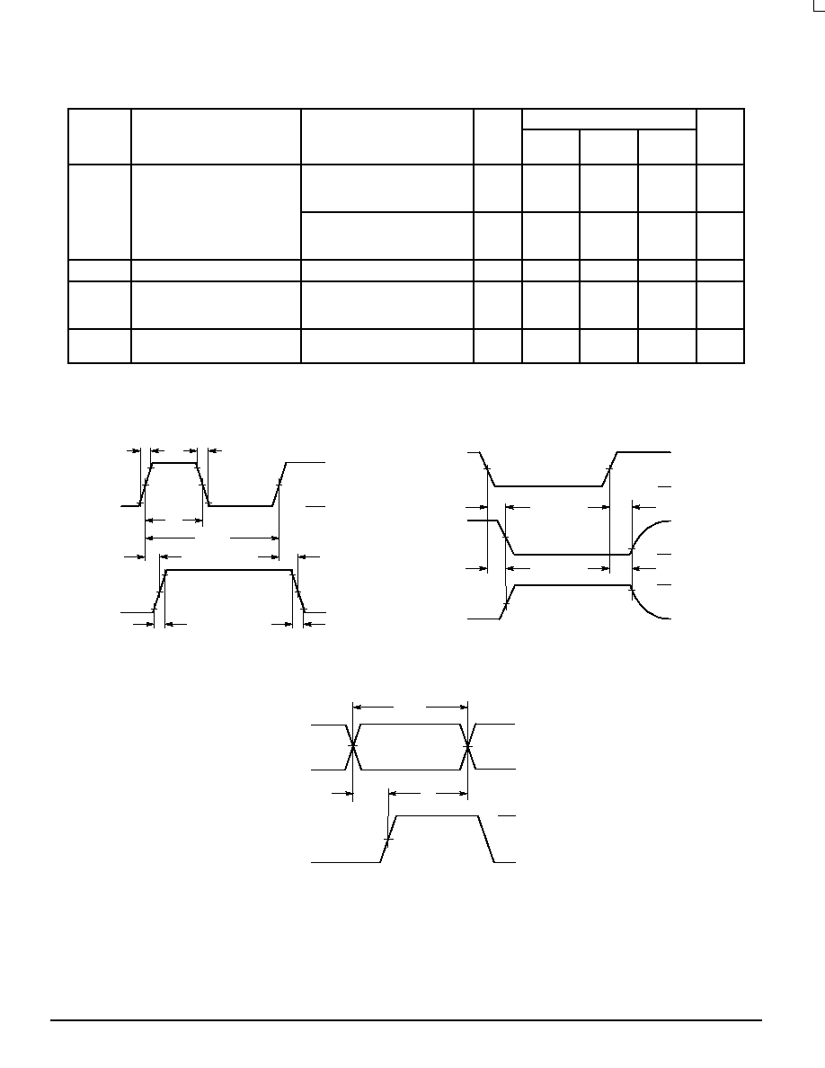
SWITCHING WAVEFORMS
Figure 1.
tr
tf
VCC
GND
tTHL
tTLH
90%
50%
10%
90%
50%
10%
CLOCK
tPLH
tPHL
Q
tW
1/fmax
50%
50%
50%
OUTPUT
ENABLE
Q
tPZL
tPLZ
tPZH tPHZ
10%
90%
VCC
GND
HIGH
IMPEDANCE
VOL
VOH
HIGH
IMPEDANCE
50%
DATA
CLOCK
VCC
VCC
GND
GND
VALID
th
tsu
50%
Q
Figure 2.
Figure 3.
MC54/74HC374A
MOTOROLA
HighSpeed CMOS Logic Data
DL129 -- Rev 6
34
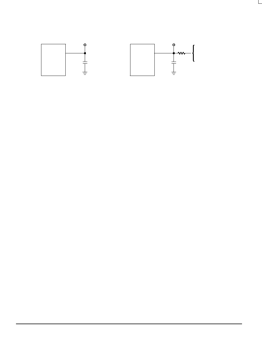
TEST CIRCUITS
Figure 4.
* Includes all probe and jig capacitance
CL*
TEST POINT
DEVICE
UNDER
TEST
OUTPUT
* Includes all probe and jig capacitance
CL*
TEST POINT
DEVICE
UNDER
TEST
OUTPUT
CONNECT TO VCC WHEN
TESTING tPLZ AND tPZL.
CONNECT TO GND WHEN
TESTING tPHZ AND tPZH.
1 k
Figure 5.
MC54/74HC374A
HighSpeed CMOS Logic Data
DL129 -- Rev 6
35
MOTOROLA
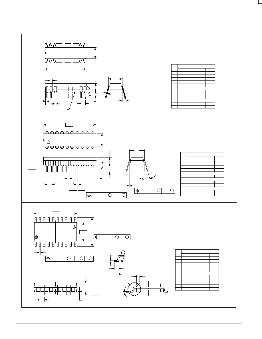
OUTLINE DIMENSIONS
J SUFFIX
CERAMIC PACKAGE
CASE 73203
ISSUE E
N SUFFIX
PLASTIC PACKAGE
CASE 73803
ISSUE E
DW SUFFIX
PLASTIC SOIC PACKAGE
CASE 751D04
ISSUE E
NOTES:
1. LEADS WITHIN 0.25 (0.010) DIAMETER, TRUE
POSITION AT SEATING PLANE, AT MAXIMUM
MATERIAL CONDITION.
2. DIMENSION L TO CENTER OF LEADS WHEN
FORMED PARALLEL.
3. DIMENSIONS A AND B INCLUDE MENISCUS.
DIM
MIN
MAX
MIN
MAX
INCHES
MILLIMETERS
A
23.88
25.15
0.940
0.990
B
6.60
7.49
0.260
0.295
C
3.81
5.08
0.150
0.200
D
0.38
0.56
0.015
0.022
F
1.40
1.65
0.055
0.065
G
2.54 BSC
0.100 BSC
H
0.51
1.27
0.020
0.050
J
0.20
0.30
0.008
0.012
K
3.18
4.06
0.125
0.160
L
7.62 BSC
0.300 BSC
M
0
15
0
15
N
0.25
1.02
0.010
0.040
_
_
_
_
A
20
1
10
11
B
F
C
SEATING
PLANE
D
H
G
K
N
J
M
L
NOTES:
1. DIMENSIONING AND TOLERANCING PER ANSI
Y14.5M, 1982.
2. CONTROLLING DIMENSION: INCH.
3. DIMENSION L TO CENTER OF LEAD WHEN
FORMED PARALLEL.
4. DIMENSION B DOES NOT INCLUDE MOLD
FLASH.
M
L
J
20 PL
M
B
M
0.25 (0.010)
T
DIM
MIN
MAX
MIN
MAX
MILLIMETERS
INCHES
A
25.66
27.17
1.010
1.070
B
6.10
6.60
0.240
0.260
C
3.81
4.57
0.150
0.180
D
0.39
0.55
0.015
0.022
G
2.54 BSC
0.100 BSC
J
0.21
0.38
0.008
0.015
K
2.80
3.55
0.110
0.140
L
7.62 BSC
0.300 BSC
M
0
15
0
15
N
0.51
1.01
0.020
0.040
_
_
_
_
E
1.27
1.77
0.050
0.070
1
11
10
20
A
SEATING
PLANE
K
N
F
G
D
20 PL
T
M
A
M
0.25 (0.010)
T
E
B
C
F
1.27 BSC
0.050 BSC
NOTES:
1. DIMENSIONING AND TOLERANCING PER
ANSI Y14.5M, 1982.
2. CONTROLLING DIMENSION: MILLIMETER.
3. DIMENSIONS A AND B DO NOT INCLUDE
MOLD PROTRUSION.
4. MAXIMUM MOLD PROTRUSION 0.150
(0.006) PER SIDE.
5. DIMENSION D DOES NOT INCLUDE
DAMBAR PROTRUSION. ALLOWABLE
DAMBAR PROTRUSION SHALL BE 0.13
(0.005) TOTAL IN EXCESS OF D DIMENSION
AT MAXIMUM MATERIAL CONDITION.
A
B
20
1
11
10
S
A
M
0.010 (0.25)
B
S
T
D
20X
M
B
M
0.010 (0.25)
P
10X
J
F
G
18X
K
C
T
SEATING
PLANE
M
R
X 45
_
DIM
MIN
MAX
MIN
MAX
INCHES
MILLIMETERS
A
12.65
12.95
0.499
0.510
B
7.40
7.60
0.292
0.299
C
2.35
2.65
0.093
0.104
D
0.35
0.49
0.014
0.019
F
0.50
0.90
0.020
0.035
G
1.27 BSC
0.050 BSC
J
0.25
0.32
0.010
0.012
K
0.10
0.25
0.004
0.009
M
0
7
0
7
P
10.05
10.55
0.395
0.415
R
0.25
0.75
0.010
0.029
_
_
_
_
MC54/74HC374A
MOTOROLA
HighSpeed CMOS Logic Data
DL129 -- Rev 6
36
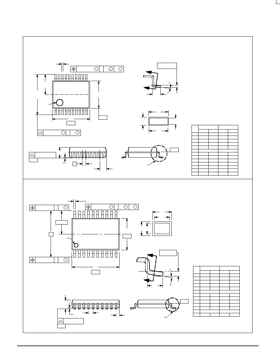
OUTLINE DIMENSIONS
DT SUFFIX
PLASTIC TSSOP PACKAGE
CASE 948E02
ISSUE A
DIM
A
MIN
MAX
MIN
MAX
INCHES
6.60
0.260
MILLIMETERS
B
4.30
4.50
0.169
0.177
C
1.20
0.047
D
0.05
0.15
0.002
0.006
F
0.50
0.75
0.020
0.030
G
0.65 BSC
0.026 BSC
H
0.27
0.37
0.011
0.015
J
0.09
0.20
0.004
0.008
J1
0.09
0.16
0.004
0.006
K
0.19
0.30
0.007
0.012
K1
0.19
0.25
0.007
0.010
L
6.40 BSC
0.252 BSC
M
0
8
0
8
_
_
_
_
NOTES:
1. DIMENSIONING AND TOLERANCING PER ANSI
Y14.5M, 1982.
2. CONTROLLING DIMENSION: MILLIMETER.
3. DIMENSION A DOES NOT INCLUDE MOLD FLASH,
PROTRUSIONS OR GATE BURRS. MOLD FLASH
OR GATE BURRS SHALL NOT EXCEED 0.15
(0.006) PER SIDE.
4. DIMENSION B DOES NOT INCLUDE INTERLEAD
FLASH OR PROTRUSION. INTERLEAD FLASH OR
PROTRUSION SHALL NOT EXCEED 0.25 (0.010)
PER SIDE.
5. DIMENSION K DOES NOT INCLUDE DAMBAR
PROTRUSION. ALLOWABLE DAMBAR
PROTRUSION SHALL BE 0.08 (0.003) TOTAL IN
EXCESS OF THE K DIMENSION AT MAXIMUM
MATERIAL CONDITION.
6. TERMINAL NUMBERS ARE SHOWN FOR
REFERENCE ONLY.
7. DIMENSION A AND B ARE TO BE DETERMINED
AT DATUM PLANE W.
ÍÍÍÍ
ÍÍÍÍ
ÍÍÍÍ
ÍÍÍÍ
1
10
11
20
PIN 1
IDENT
A
B
T
0.100 (0.004)
C
D
G
H
SECTION NN
K
K1
J J1
N
N
M
F
W
SEATING
PLANE
V
U
S
U
M
0.10 (0.004)
V
S
T
20X REF
K
L
L/2
2X
S
U
0.15 (0.006) T
DETAIL E
0.25 (0.010)
DETAIL E
6.40
0.252
S
U
0.15 (0.006) T
SD SUFFIX
PLASTIC SSOP PACKAGE
CASE 940C03
ISSUE B
20
11
10
1
H
A
B
F
M
K
20X REF
S
U
M
0.12 (0.005)
V
S
T
L
L/2
PIN 1
IDENT
S
U
M
0.20 (0.008)
T
V
U
D
C
0.076 (0.003)
G
T
SEATING
PLANE
DETAIL E
N
N
0.25 (0.010)
ÇÇÇ
ÇÇÇ
ÇÇÇ
ÇÇÇ
ÉÉÉ
ÉÉÉ
ÉÉÉ
ÉÉÉ
K
J
J1
K1
SECTION NN
DIM
A
MIN
MAX
MIN
MAX
INCHES
7.07
7.33
0.278
0.288
MILLIMETERS
B
5.20
5.38
0.205
0.212
C
1.73
1.99
0.068
0.078
D
0.05
0.21
0.002
0.008
F
0.63
0.95
0.024
0.037
G
0.65 BSC
0.026 BSC
H
0.59
0.75
0.023
0.030
J
0.09
0.20
0.003
0.008
J1
0.09
0.16
0.003
0.006
K
0.25
0.38
0.010
0.015
K1
0.25
0.33
0.010
0.013
_
_
_
_
NOTES:
1. DIMENSIONING AND TOLERANCING PER ANSI
Y14.5M, 1982.
2. CONTROLLING DIMENSION: MILLIMETER.
3. DIMENSION A DOES NOT INCLUDE MOLD FLASH,
PROTRUSIONS OR GATE BURRS. MOLD FLASH OR
GATE BURRS SHALL NOT EXCEED 0.15 (0.006) PER
SIDE.
4. DIMENSION B DOES NOT INCLUDE INTERLEAD
FLASH OR PROTRUSION. INTERLEAD FLASH OR
PROTRUSION SHALL NOT EXCEED 0.15 (0.006) PER
SIDE.
5. DIMENSION K DOES NOT INCLUDE DAMBAR
PROTRUSION/INTRUSION. ALLOWABLE DAMBAR
PROTRUSION SHALL BE 0.13 (0.005) TOTAL IN
EXCESS OF K DIMENSION AT MAXIMUM MATERIAL
CONDITION. DAMBAR INTRUSION SHALL NOT
REDUCE DIMENSION K BY MORE THAN 0.07 (0.002)
AT LEAST MATERIAL CONDITION.
6. TERMINAL NUMBERS ARE SHOWN FOR REFERENCE
ONLY.
7. DIMENSION A AND B ARE TO BE DETERMINED AT
DATUM PLANE W.
L
7.65
7.90
0.301
0.311
M
0
8
0
8
DETAIL E
W
MC54/74HC374A
HighSpeed CMOS Logic Data
DL129 -- Rev 6
37
MOTOROLA
How to reach us:
USA/EUROPE: Motorola Literature Distribution;
JAPAN: Nippon Motorola Ltd.; TatsumiSPDJLDC, Toshikatsu Otsuki,
P.O. Box 20912; Phoenix, Arizona 85036. 18004412447
6F SeibuButsuryuCenter, 3142 Tatsumi KotoKu, Tokyo 135, Japan. 0335218315
MFAX: RMFAX0@email.sps.mot.com TOUCHTONE (602) 2446609
HONG KONG: Motorola Semiconductors H.K. Ltd.; 8B Tai Ping Industrial Park,
INTERNET: http://DesignNET.com
51 Ting Kok Road, Tai Po, N.T., Hong Kong. 85226629298
Motorola reserves the right to make changes without further notice to any products herein. Motorola makes no warranty, representation or guarantee regarding
the suitability of its products for any particular purpose, nor does Motorola assume any liability arising out of the application or use of any product or circuit,
and specifically disclaims any and all liability, including without limitation consequential or incidental damages. "Typical" parameters can and do vary in different
applications. All operating parameters, including "Typicals" must be validated for each customer application by customer's technical experts. Motorola does
not convey any license under its patent rights nor the rights of others. Motorola products are not designed, intended, or authorized for use as components in
systems intended for surgical implant into the body, or other applications intended to support or sustain life, or for any other application in which the failure of
the Motorola product could create a situation where personal injury or death may occur. Should Buyer purchase or use Motorola products for any such
unintended or unauthorized application, Buyer shall indemnify and hold Motorola and its officers, employees, subsidiaries, affiliates, and distributors harmless
against all claims, costs, damages, and expenses, and reasonable attorney fees arising out of, directly or indirectly, any claim of personal injury or death
associated with such unintended or unauthorized use, even if such claim alleges that Motorola was negligent regarding the design or manufacture of the part.
Motorola and
are registered trademarks of Motorola, Inc. Motorola, Inc. is an Equal Opportunity/Affirmative Action Employer.
MC54/74HC374A/D
*MC54/74HC374A/D*
CODELINE