
5-1
FACT DATA
Octal D Type Flip Flop
with 3 State Outputs
The MC74AC574/74ACT574 is a high-speed, low power octal flip-flop with a
buffered common Clock (CP) and a buffered common Output Enable (OE). The
information presented to the D inputs is stored in the flip-flops on the LOW-to-HIGH
Clock (CP) transition.
The MC74AC574/74ACT574 is functionally identical to the MC74AC374/
74ACT374 except for the pinouts.
·
Inputs and Outputs on Opposite Sides of Package
Allowing Easy Interface with Microprocessors
·
Useful as Input or Output Port for Microprocessors
·
Functionally Identical to MC74AC374/74ACT374
·
3-State Outputs for Bus-Oriented Applications
·
Outputs Source/Sink 24 mA
·
ACT574 Has TTL Compatible Inputs
19
20
18
17
16
15
14
2
1
3
4
5
6
7
VCC
13
8
12
9
11
10
O0
O1
O2
O3
O4
O5
O6
O7
CP
OE
D0
D1
D2
D3
D4
D5
D6
D7
GND
PIN NAMES
D0D7
Data Inputs
CP
Clock Pulse Input
OE
3-State Output Enable Input
O0O7
3-State Outputs
MC74AC57
MC74ACT574
OCTAL D-TYPE
FLIP-FLOP WITH
3-STATE OUTPUTS
N SUFFIX
CASE 738-03
PLASTIC
DW SUFFIX
CASE 751D-04
PLASTIC
LOGIC SYMBOL
O0 O1 O2 O3 O4 O5 O6 O7
D0 D1 D2 D3 D4 D5 D6 D7
CP
OE
MC74AC57 MC74ACT574
5-2
FACT DATA
FUNCTIONAL DESCRIPTION
The MC74AC574/74ACT574 consists of eight edge-
triggered flip-flops with individual D-type inputs and 3-state
true outputs. The buffered clock and buffered Output Enable
are common to all flip-flops. The eight flip-flops will store the
state of their individual D inputs that meet the setup and hold
time requirements on the LOW-to-HIGH Clock (CP) transition.
With the Output Enable (OE) LOW, the contents of the eight
flip-flops are available at the outputs. When OE is HIGH, the
outputs go to the high impedance state. Operation of the OE
input does not affect the state of the flip-flops.
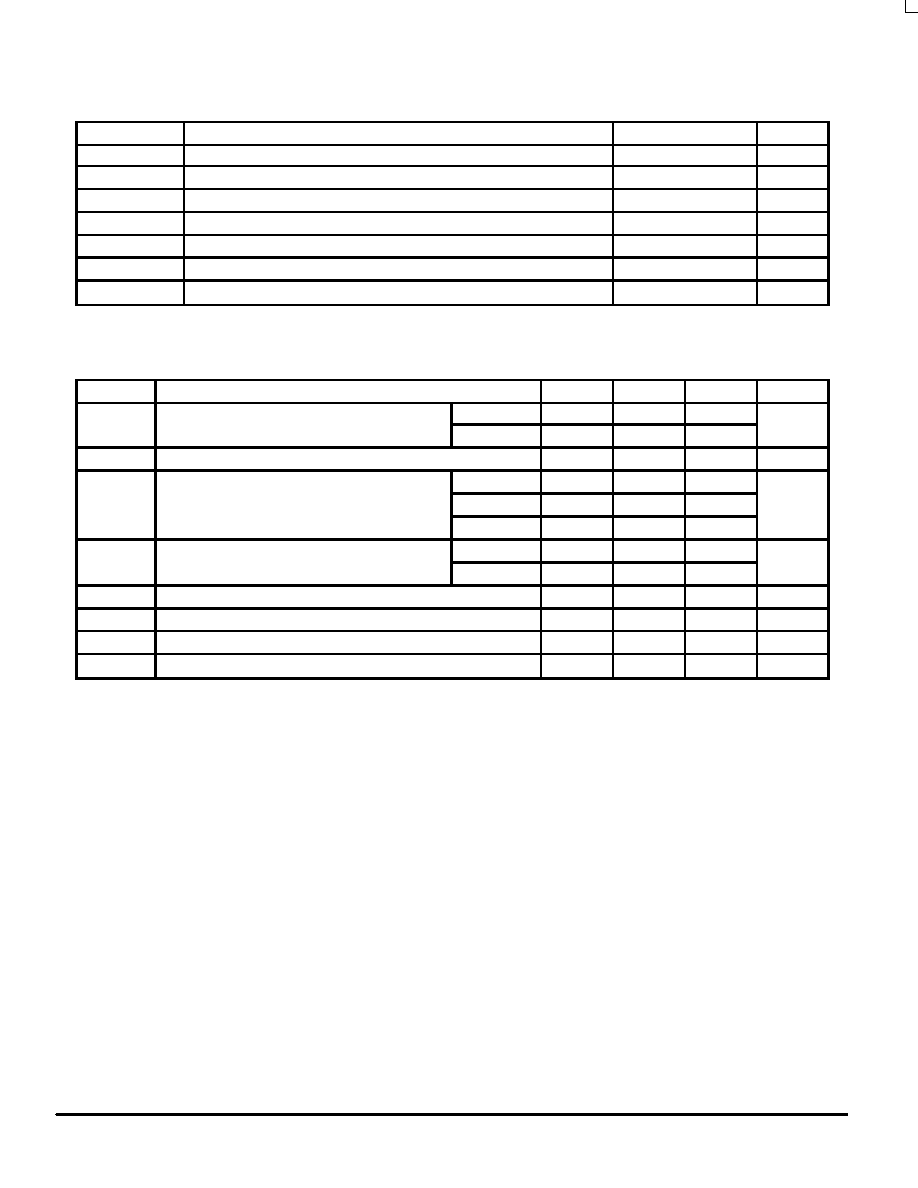
FUNCTION TABLE
Inputs
Internal
Outputs
Function
OE
CP
D
Q
On
Function
H
H
L
NC
Z
Hold
H
H
H
NC
Z
Hold
H
L
L
Z
Load
H
H
H
Z
Load
L
L
L
L
Data Available
L
H
H
H
Data Available
L
H
L
NC
NC
No Change in Data
L
H
H
NC
NC
No Change in Data
H = HIGH Voltage Level
L = LOW Voltage Level
X = Immaterial
Z = High Impedance
= LOW-to-HIGH Clock Transition
NC = No Change
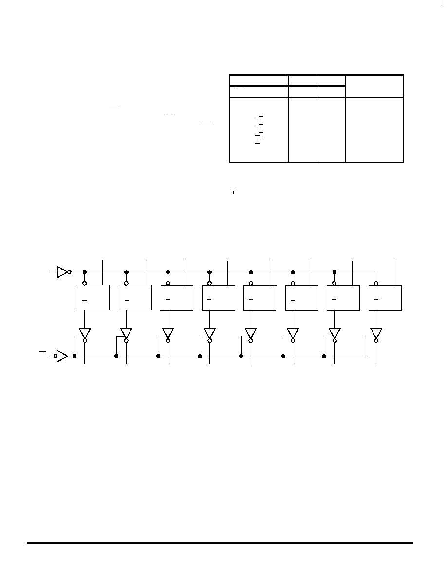
LOGIC DIAGRAM
D0
D1
D2
D3
D4
D5
D6
D7
C
D
Q
O0
O1
O2
O3
O4
O5
O6
O7
OE
CP
C
D
Q
C
D
Q
C
D
Q
C
D
Q
C
D
Q
C
D
Q
C
D
Q
Please note that this diagram is provided only for the understanding of logic
operations and should not be used to estimate propagation delays.
MC74AC57 MC74ACT574
5-3
FACT DATA
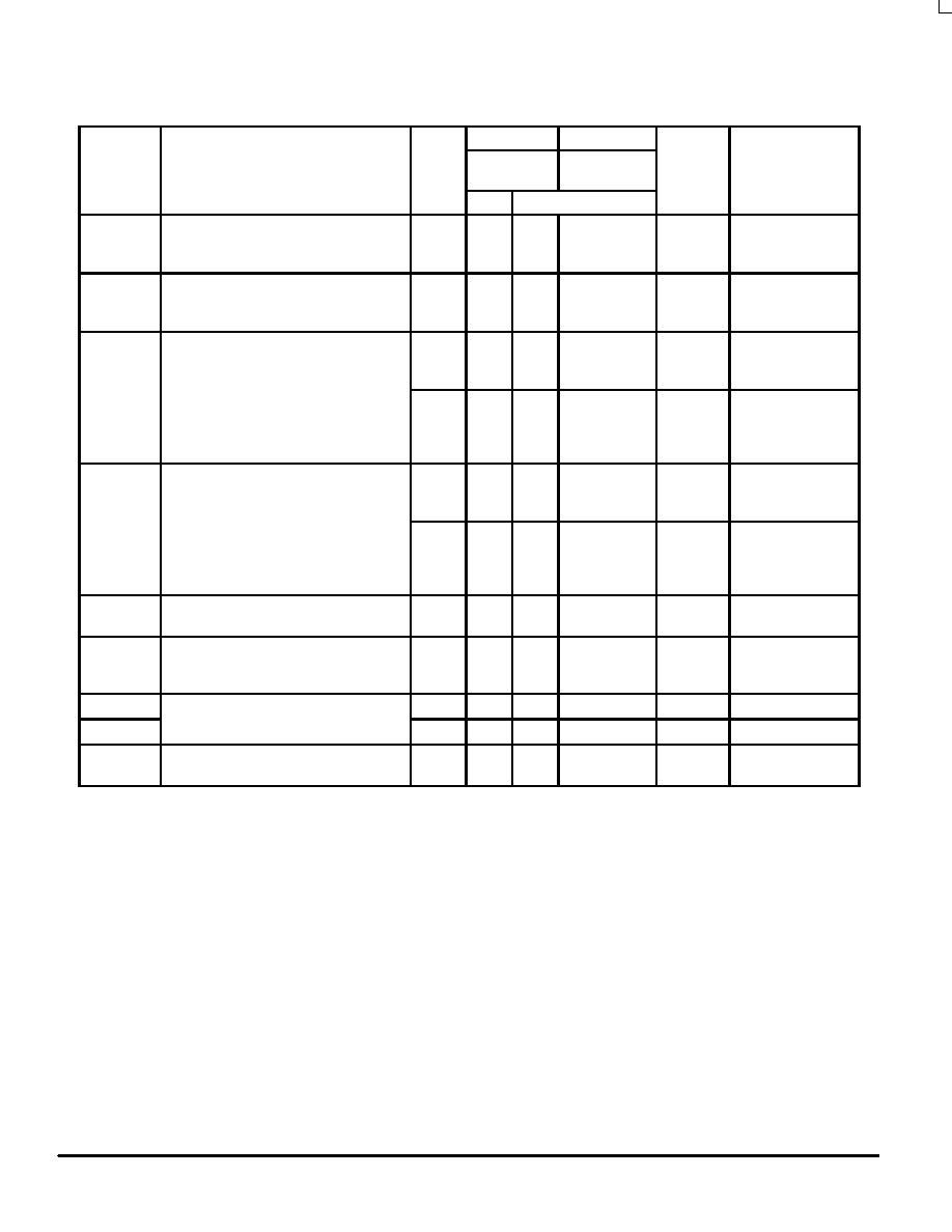
MAXIMUM RATINGS*
Symbol
Parameter
Value
Unit
VCC
DC Supply Voltage (Referenced to GND)
0.5 to +7.0
V
Vin
DC Input Voltage (Referenced to GND)
0.5 to VCC +0.5
V
Vout
DC Output Voltage (Referenced to GND)
0.5 to VCC +0.5
V
Iin
DC Input Current, per Pin
±
20
mA
Iout
DC Output Sink/Source Current, per Pin
±
50
mA
ICC
DC VCC or GND Current per Output Pin
±
50
mA
Tstg
Storage Temperature
65 to +150
°
C
* Maximum Ratings are those values beyond which damage to the device may occur. Functional operation should be restricted to the Recommended
Operating Conditions.
RECOMMENDED OPERATING CONDITIONS
Symbol
Parameter
Min
Typ
Max
Unit
VCC
Supply Voltage
AC
2.0
5.0
6.0
V
VCC
Supply Voltage
ACT
4.5
5.0
5.5
V
Vin, Vout
DC Input Voltage, Output Voltage (Ref. to GND)
0
VCC
V
tr, tf
Input Rise and Fall Time (Note 1)
AC Devices except Schmitt Inputs
VCC @ 3.0 V
150
tr, tf
Input Rise and Fall Time (Note 1)
AC Devices except Schmitt Inputs
VCC @ 4.5 V
40
ns/V
r, tf
AC Devices except Schmitt Inputs
VCC @ 5.5 V
25
tr, tf
Input Rise and Fall Time (Note 2)
ACT Devices except Schmitt Inputs
VCC @ 4.5 V
10
ns/V
tr, tf
Input Rise and Fall Time (Note 2)
ACT Devices except Schmitt Inputs
VCC @ 5.5 V
8.0
ns/V
TJ
Junction Temperature (PDIP)
140
°
C
TA
Operating Ambient Temperature Range
40
25
85
°
C
IOH
Output Current -- High
24
mA
IOL
Output Current -- Low
24
mA
1. Vin from 30% to 70% VCC; see individual Data Sheets for devices that differ from the typical input rise and fall times.
2. Vin from 0.8 V to 2.0 V; see individual Data Sheets for devices that differ from the typical input rise and fall times.
MC74AC57 MC74ACT574
5-4
FACT DATA
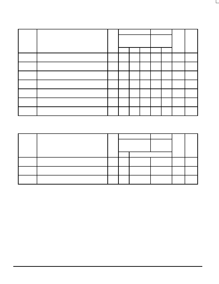
DC CHARACTERISTICS
Symbol
Parameter
VCC
(V)
74AC
74AC
Unit
Conditions
Symbol
Parameter
VCC
(V)
TA = +25
°
C
TA =
40
°
C to +85
°
C
Unit
Conditions
Typ
Guaranteed Limits
VIH
Minimum High Level
Input Voltage
3.0
1.5
2.1
2.1
VOUT = 0.1 V
Input Voltage
4.5
2.25
3.15
3.15
V
or VCC 0.1 V
5.5
2.75
3.85
3.85
VIL
Maximum Low Level
Input Voltage
3.0
1.5
0.9
0.9
VOUT = 0.1 V
Input Voltage
4.5
2.25
1.35
1.35
V
or VCC 0.1 V
5.5
2.75
1.65
1.65
VOH
Minimum High Level
Output Voltage
3.0
2.99
2.9
2.9
IOUT = 50
µ
A
Output Voltage
4.5
4.49
4.4
4.4
V
5.5
5.49
5.4
5.4
V
*VIN = VIL or VIH
3.0
2.56
2.46
V
12 mA
4.5
3.86
3.76
V
IOH
24 mA
5.5
4.86
4.76
24 mA
VOL
Maximum Low Level
Output Voltage
3.0
0.002
0.1
0.1
IOUT = 50
µ
A
Output Voltage
4.5
0.001
0.1
0.1
V
5.5
0.001
0.1
0.1
V
*VIN = VIL or VIH
3.0
0.36
0.44
V
12 mA
4.5
0.36
0.44
V
IOL
24 mA
5.5
0.36
0.44
24 mA
IIN
Maximum Input
Leakage Current
5.5
±
0.1
±
1.0
µ
A
VI = VCC, GND
Leakage Current
5.5
±
0.1
±
1.0
µ
A
VI = VCC, GND
IOZ
Maximum
3-State
Current
VI (OE) = VIL, VIH
3-State
Current
5.5
±
0.5
±
5.0
µ
A
VI = VCC, GND
Current
VO = VCC, GND
IOLD
Minimum Dynamic
Output Current
5.5
75
mA
VOLD = 1.65 V Max
IOHD
Output Current
5.5
75
mA
VOHD = 3.85 V Min
ICC
Maximum Quiescent
Supply Current
5.5
8.0
80
µ
A
VIN = VCC or GND
Supply Current
5.5
8.0
80
µ
A
VIN = VCC or GND
* All outputs loaded; thresholds on input associated with output under test.
Maximum test duration 2.0 ms, one output loaded at a time.
Note: IIN and ICC @ 3.0 V are guaranteed to be less than or equal to the respective limit @ 5.5 V VCC.
MC74AC57 MC74ACT574
5-5
FACT DATA
AC CHARACTERISTICS (For Figures and Waveforms -- See Section 3)
Symbol
Parameter
VCC*
(V)
74AC
74AC
Unit
Fig.
No.
Symbol
Parameter
VCC*
(V)
TA = +25
°
C
CL = 50 pF
TA = 40
°
C
to +85
°
C
CL = 50 pF
Unit
Fig.
No.
Min
Typ
Max
Min
Max
fmax
Maximum Clock
3.3
75
60
MHz
3-3
fmax
Frequency
5.0
95
85
MHz
3-3
tPLH
Propagation Delay
3.3
3.5
13.5
3.5
15
ns
3-6
tPLH
CP to On
5.0
2.0
9.5
2.0
11
ns
3-6
tPHL
Propagation Delay
3.3
3.5
12
3.5
13.5
ns
3-6
tPHL
CP to On
5.0
2.0
8.5
2.0
9.5
ns
3-6
tPZH
Output Enable Time
3.3
2.5
11
2.5
12
ns
3-7
tPZH
Output Enable Time
5.0
2.0
8.5
2.0
9.0
ns
3-7
tPZL
Output Enable Time
3.3
3.0
10.5
3.5
11.5
ns
3-8
tPZL
Output Enable Time
5.0
1.5
8.0
2.0
9.0
ns
3-8
tPHZ
Output Disable Time
3.3
4.0
12
4.5
13
ns
3-7
tPHZ
Output Disable Time
5.0
2.0
9.5
2.0
10.5
ns
3-7
tPLZ
Output Disable Time
3.3
2.0
9.0
2.5
10
ns
3-8
tPLZ
Output Disable Time
5.0
1.5
7.5
1.5
8.5
ns
3-8
* Voltage Range 3.3 V is 3.3 V
±
0.3 V.
Voltage Range 5.0 V is 5.0 V
±
0.5 V.
AC OPERATING REQUIREMENTS
Symbol
Parameter
VCC*
(V)
74AC
74AC
Unit
Fig.
No.
Symbol
Parameter
VCC*
(V)
TA = +25
°
C
CL = 50 pF
TA = 40
°
C
to +85
°
C
CL = 50 pF
Unit
Fig.
No.
Typ
Guaranteed Minimum
ts
Setup Time, HIGH or LOW
3.3
2.5
3.0
ns
3-9
ts
Dn to CP
5.0
1.5
2.0
ns
3-9
th
Hold Time, HIGH or LOW
3.3
1.5
1.5
ns
3-9
th
Dn to CP
5.0
1.5
1.5
ns
3-9
tw
CP Pulse Width
3.3
6.0
7.0
ns
3-6
tw
HIGH or LOW
5.0
4.0
5.0
ns
3-6
* Voltage Range 3.3 V is 3.3 V
±
0.3 V.
Voltage Range 5.0 V is 5.0 V
±
0.5 V.