Äîêóìåíòàöèÿ è îïèñàíèÿ www.docs.chipfind.ru
MC34129
MC33129
SEMICONDUCTOR
TECHNICAL DATA
HIGH PERFORMANCE
CURRENT MODE
CONTROLLERS
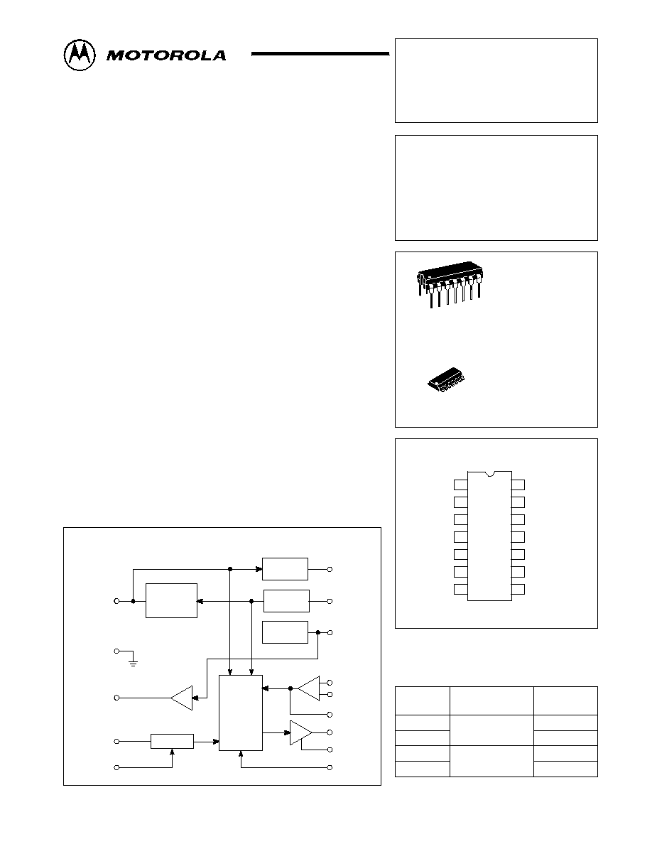
PIN CONNECTIONS
Order this document by MC34129/D
D SUFFIX
PLASTIC PACKAGE
CASE 751A
(SO14)
P SUFFIX
PLASTIC PACKAGE
CASE 646
14
1
14
1
(Top View)
Drive Output
Drive Ground
Ramp Input
Sync/Inhibit
Input
RT/CT
Vref 2.5 V
Gnd
1
2
3
4
5
6
7
8
9
10
11
12
13
14 VCC
Start/Run Output
CSoftStart
Feedback/
PWM Input
Error Amp
Inverting Input
Error Amp
Noninverting Input
Vref 1.25 V
Device
Operating
Temperature Range
Package
ORDERING INFORMATION
MC34129D
MC34129P
TA = 0
°
to +70
°
C
SO14
Plastic DIP
MC33129D
MC33129P
SO14
Plastic DIP
TA = 40
°
to +85
°
C
1
MOTOROLA ANALOG IC DEVICE DATA
High Performance
Current Mode Controllers
The MC34129/MC33129 are high performance current mode switching
regulators specifically designed for use in low power digital telephone
applications. These integrated circuits feature a unique internal fault timer
that provides automatic restart for overload recovery. For enhanced system
efficiency, a start/run comparator is included to implement bootstrapped
operation of VCC. Other functions contained are a temperature compensated
reference, reference amplifier, fully accessible error amplifier, sawtooth
oscillator with sync input, pulse width modulator comparator, and a high
current totem pole driver ideally suited for driving a power MOSFET.
Also included are protective features consisting of softstart,
undervoltage lockout, cyclebycycle current limiting, adjustable deadtime,
and a latch for single pulse metering.
Although these devices are primarily intended for use in digital telephone
systems, they can be used cost effectively in many other applications.
·
Current Mode Operation to 300 kHz
·
Automatic Feed Forward Compensation
·
Latching PWM for CyclebyCycle Current Limiting
·
Continuous Retry after Fault Timeout
·
SoftStart with Maximum Peak Switch Current Clamp
·
Internally Trimmed 2% Bandgap Reference
·
High Current Totem Pole Driver
·
Input Undervoltage Lockout
·
Low Startup and Operating Current
·
Direct Interface with Motorola SENSEFET Products
Simplified Block Diagram
+
SoftStart
and
Fault Timer
Start/Run
Undervoltage
Lockout
1.25V
Reference
Error Amp
Latching
PWM
X2
Oscillator
12
7
6
5
4
CSoftStart
Gnd
Vref 2.5V
RT/CT
Sync/Inhibit
Input
13
14
8
9
10
11
1
2
3
Start/Run
Output
VCC
Vref 1.25V
Noninverting
Input
Inverting
Input
Feedback/
PWM Input
Drive Out
Drive Gnd
Ramp Input
©
Motorola, Inc. 1996
Rev 1
MC34129 MC33129
2
MOTOROLA ANALOG IC DEVICE DATA
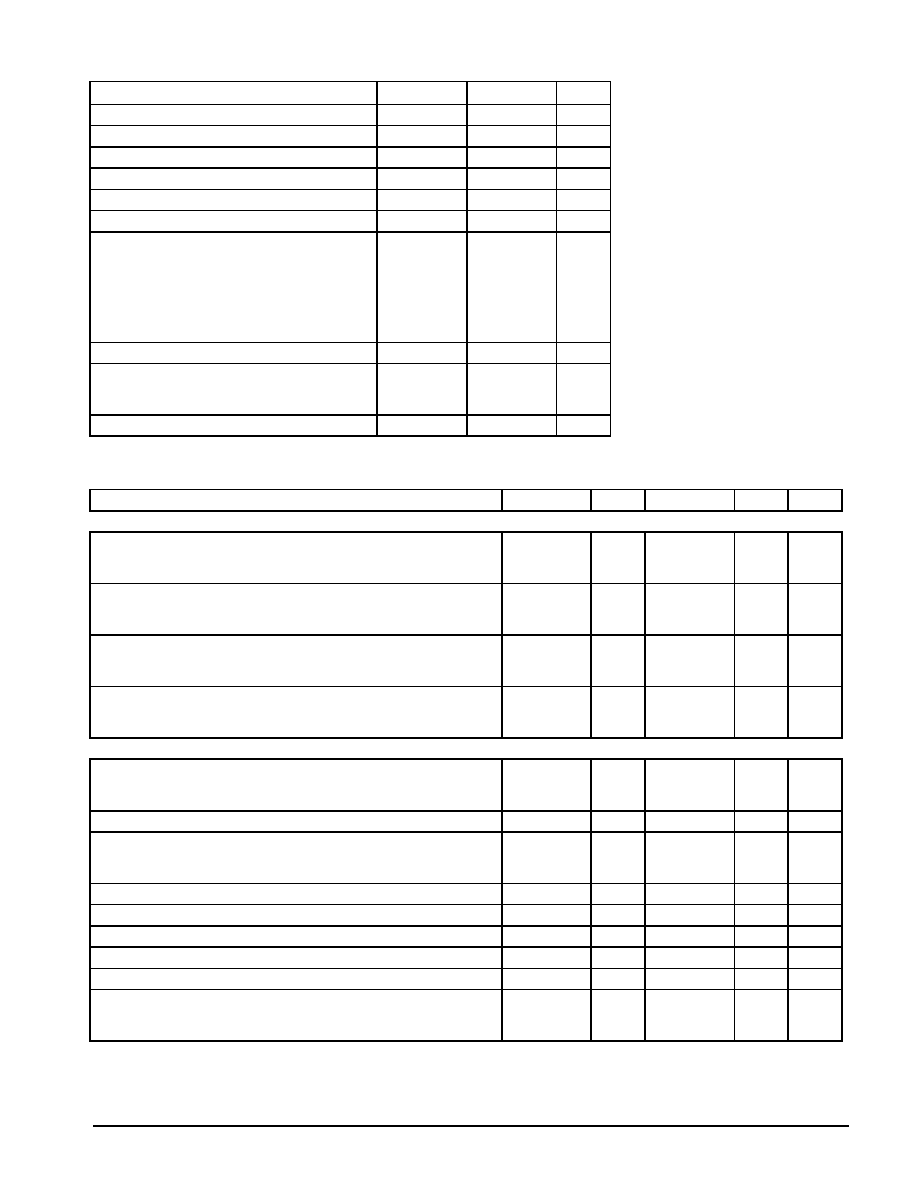
MAXIMUM RATINGS
Rating
Symbol
Value
Unit
VCC Zener Current
IZ(VCC)
50
mA
Start/Run Output Zener Current
IZ(Start/Run)
50
mA
Analog Inputs (Pins 3, 5, 9, 10, 11, 12)
0.3 to 5.5
V
Sync Input Voltage
Vsync
0.3 to VCC
V
Drive Output Current, Source or Sink
IDRV
1.0
A
Current, Reference Outputs (Pins 6, 8)
Iref
20
mA
Power Dissipation and Thermal Characteristics
D Suffix, Plastic Package Case 751A
Maximum Power Dissipation @ TA = 70
°
C
Thermal Resistance, JunctiontoAir
P Suffix, Plastic Package Case 646
Maximum Power Dissipation @ TA = 70
°
C
Thermal Resistance, JunctiontoAir
PD
R
JA
PD
R
JA
552
145
800
100
mW
°
C/W
mW
°
C/W
Operating Junction Temperature
TJ
+150
°
C
Operating Ambient Temperature
MC34129
MC33129
TA
0 to +70
40 to +85
°
C
Storage Temperature Range
Tstg
65 to +150
°
C
ELECTRICAL CHARACTERISTICS
(VCC = 10 V, TA = 25
°
C [Note 1], unless otherwise noted.)
Characteristics
Symbol
Min
Typ
Max
Unit
REFERENCE SECTIONS
Reference Output Voltage, TA = 25
°
C
1.25 V Ref., IL = 0 mA
2.50 V Ref., IL = 1.0 mA
Vref
1.225
2.375
1.250
2.500
1.275
2.625
V
Reference Output Voltage, TA = Tlow to Thigh
1.25 V Ref., IL = 0 mA
2.50 V Ref., IL = 1.0 mA
Vref
1.200
2.250
1.300
2.750
V
Line Regulation (VCC = 4.0 V to 12 V)
1.25 V Ref., IL = 0 mA
2.50 V Ref., IL = 1.0 mA
Regline
2.0
10
12
50
mV
Load Regulation
1.25 V Ref., IL = 10
µ
A to +500
µ
A
2.50 V Ref., IL = 0.1 mA to +1.0 mA
Regload
1.0
3.0
12
25
mV
ERROR AMPLIFIER
Input Offset Voltage (Vin = 1.25 V)
TA = 25
°
C
TA = Tlow to Thigh
VIO
1.5
10
mV
Input Offset Current (Vin = 1.25 V)
IIO
10
nA
Input Bias Current (Vin = 1.25 V)
TA = 25
°
C
TA = Tlow to Thigh
IIB
25
200
nA
Input Common Mode Voltage Range
VICR
0.5 to 5.5
V
Open Loop Voltage Gain (VO = 1.25 V)
AVOL
65
87
dB
Gain Bandwidth Product (VO = 1.25 V, f = 100 kHz)
GBW
500
750
kHz
Power Supply Rejection Ratio (VCC = 5.0 V to 10 V)
PSRR
65
85
dB
Output Source Current (VO = 1.5 V)
ISource
40
80
µ
A
Output Voltage Swing
High State (ISource = 0
µ
A)
Low State (ISink = 500
µ
A)
VOH
VOL
1.75
1.96
0.1
2.25
0.15
V
NOTE:
1. Tlow = 0
°
C for MC34129
Thigh = +70
°
C for MC34129
40
°
C for MC33129
+85
°
C for MC33129
MC34129 MC33129
3
MOTOROLA ANALOG IC DEVICE DATA
ELECTRICAL CHARACTERISTICS
(VCC = 10 V, TA = 25
°
C [Note 1], unless otherwise noted.)
Characteristics
Symbol
Min
Typ
Max
Unit
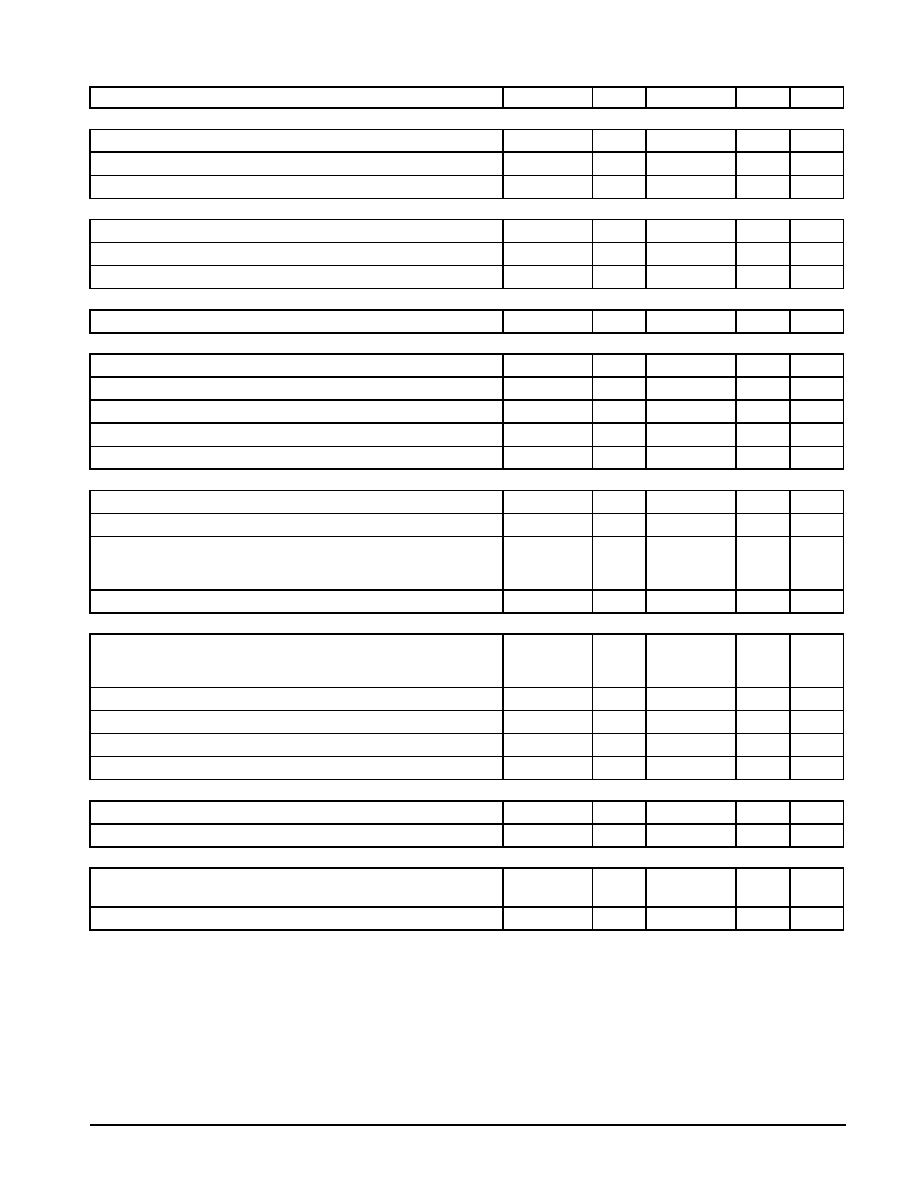
PWM COMPARATOR
Input Offset Voltage (Vin = 1.25 V)
VIO
150
275
400
mV
Input Bias Current
IIB
120
250
µ
A
Propagation Delay, Ramp Input to Drive Output
tPLH(IN/DRV)
250
ns
SOFTSTART
Capacitor Charge Current (Pin 12 = 0 V)
Ichg
0.75
1.2
1.50
µ
A
Buffer Input Offset Voltage (Vin = 1.25 V)
VIO
15
40
mV
Buffer Output Voltage (ISink = 100
µ
A)
VOL
0.15
0.225
V
FAULT TIMER
Restart Delay Time
tDLY
200
400
600
µ
s
START/RUN COMPARATOR
Threshold Voltage (Pin 12)
Vth
2.0
V
Threshold Hysteresis Voltage (Pin 12)
VH
350
mV
Output Voltage (ISink = 500
µ
A)
VOL
9.0
10
10.3
V
Output OffState Leakage Current (VOH = 15 V)
IS/R(leak)
0.4
2.0
µ
A
Output Zener Voltage (IZ = 10 mA)
VZ
(VCC + 7.6)
V
OSCILLATOR
Frequency (RT = 25.5 k
, CT = 390 pF)
fOSC
80
100
120
kHz
Capacitor CT Discharge Current (Pin 5 = 1.2 V)
Idischg
240
350
460
µ
A
Sync Input Current
High State (Vin = 2.0 V)
Low State (Vin = 0.8 V)
IIH
IIL
40
15
125
35
µ
A
Sync Input Resistance
Rin
12.5
32
50
k
DRIVE OUTPUT
Output Voltage
High State (ISource = 200 mA)
Low State (ISource = 200 mA)
VOH
VOL
8.3
8.9
1.4
1.8
V
Low State Holding Current
IH
225
µ
A
Output Voltage Rise Time (CL = 500 pF)
tr
390
ns
Output Voltage Fall Time (CL = 500 pF)
tf
30
ns
Output PullDown Resistance
RPD
100
225
350
k
UNDERVOLTAGE LOCKOUT
Startup Threshold
Vth
3.0
3.6
4.2
V
Hysteresis
VH
5.0
10
15
%
TOTAL DEVICE
Power Supply Current
RT = 25.5 k
, CT = 390 pF, CL = 500 pF
ICC
1.0
2.5
4.0
mA
Power Supply Zener Voltage (IZ = 10 mA)
VZ
12
14.3
V
NOTE:
1. Tlow = 0
°
C for MC34129
Thigh = +70
°
C for MC34129
40
°
C for MC33129
+85
°
C for MC33129
MC34129 MC33129
4
MOTOROLA ANALOG IC DEVICE DATA
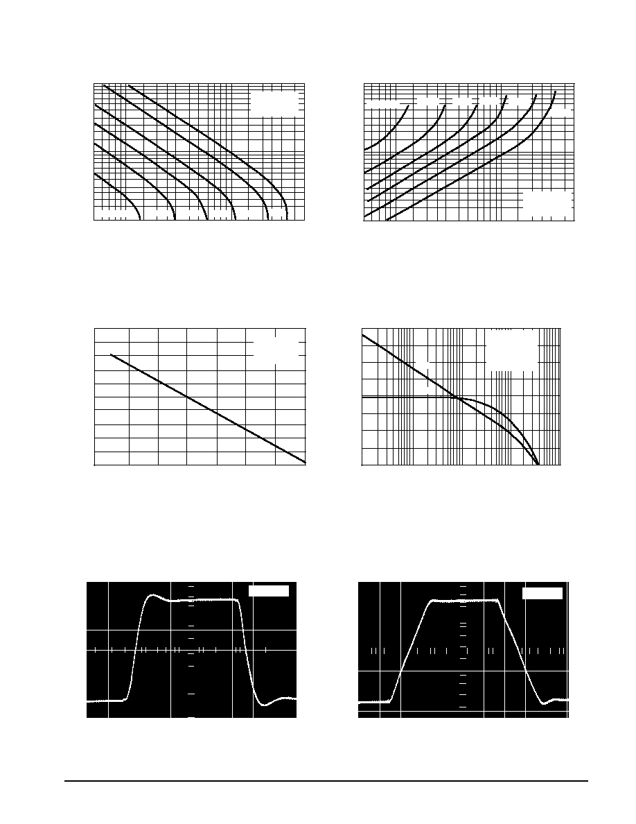
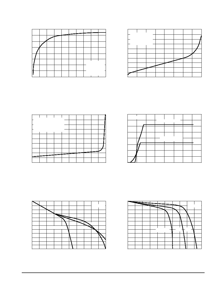
Figure 1. Timing Resistor versus
Oscillator Frequency
Figure 2. Output Deadtime versus
Oscillator Frequency
Figure 3. Oscillator Frequency Change
versus Temperature
Figure 4. Error Amp Open Loop Gain and
Phase versus Frequency
Figure 5. Error Amp SmallSignal
Transient Response
Figure 6. Error Amp LargeSignal
Transient Response
0.5
µ
s/DIV
20 mV/DIV
200 mV/DIV
1.0
µ
s/DIV
TA = 25
°
C
fOSC, OSCILLATOR FREQUENCY (kHz)
R
T
, TIMING RESIST
OR
(
)
CT = 5.0 nF
2.0 nF
1.0 nF
500 pF
200 pF
100pF
f OSC
, OSCILLA
T
OR
FREQUENCY
CHANGE (%)
TA, AMBIENT TEMPERATURE (
°
C)
VCC = 10 V
RT = 25.5 k
CT = 390 pF
fOSC, OSCILLATOR FREQUENCY (kHz)
%DT
, PERCENT
OUTPUT
DEADTIME
CT = 5.0 nF
2.0 nF
1.0 nF
200 pF
100 pF
f, FREQUENCY (Hz)
A
VOL
, OPEN LOOP
VOL
T
AGE GAIN (dB)
0
45
90
135
180
, EXCESS PHASE (DEGREES)
Gain
Phase
TA = 25
°
C
5.0
10
20
50
100
200
500
55
25
0
25
50
75
100
125
5.0
10
20
50
100
200
500
1.0 k
10 k
100 k
1.0 M
10 M
1.05 V
1.0 V
0.95 V
1.5 V
1.0 V
0.5 V
1.0 M
500 k
200 k
100 k
50 k
20 k
10 k
8.0
4.0
0
4.0
8.0
100
50
20
5.0
2.0
1.0
60
40
20
0
20
VCC = 10 V
TA = 25
°
C
VCC = 10 V
TA = 25
°
C
500 pF
VCC = 10 V
VO = 1.25 V
RL =
TA = 25
°
C
MC34129 MC33129
5
MOTOROLA ANALOG IC DEVICE DATA
Figure 7. Error Amp Open Loop DC Gain
versus Load Resistance
Figure 8. Error Amp Output Saturation
versus Sink Current
Figure 9. SoftStart Buffer Output Saturation
versus Sink Current
Figure 10. Reference Output Voltage versus
Supply Voltage
Figure 11. 1.25 V Reference Output Voltage
Change versus Source Current
Figure 12. 2.5 V Reference Output Voltage
Change versus Source Current
RL, OUTPUT LOAD RESISTANCE (k
)
A
VOL
, OPEN LOOP
VOL
T
AGE GAIN (dB)
VCC = 10 V
VO = 1.25 V
RL to 1.25 Vref
TA = 25
°
C
ISink, OUTPUT SINK CURRENT (mA)
V
sat
, OUTPUT
SA
TURA
TION VOL
T
AGE
(V)
VCC = 10 V
Pins 8 to 9, 6 to 10
Pins 2, 5, 7 to Gnd
TA = 25
°
C
V
sat
, OUTPUT
SA
TURA
TION VOL
T
AGE
(V)
ISink, OUTPUT SINK CURRENT (
µ
A)
VCC, SUPPLY VOLTAGE (V)
V
ref
, REFERENCE OUTPUT
VOL
T
AGE (V)
TA = 25
°
C
Vref 2.5 V, RL = 2.5 k
Iref, REFERENCE OUTPUT SOURCE CURRENT (mA)
V
ref
, REFERENCE OUTPUT
VOL
T
AGE CHANGE (mV)
TA = 40
°
C
VCC = 10 V
+85
°
C
+25
°
C
Iref, REFERENCE OUTPUT SOURCE CURRENT (mA)
V
ref
, REFERENCE OUTPUT
VOL
T
AGE CHANGE (mV)
TA = 40
°
C
VCC = 10 V
85
°
C
25
°
C
90
80
70
60
50
1.0
0.8
0.6
0.4
0.2
0
1.0
0.8
0.6
0.4
0.2
0
3.2
2.4
1.6
0.8
0
0
4.0
8.0
12
16
20
24
0
4.0
8.0
12
16
20
24
0
20
40
60
80
100
0
2.0
4.0
6.0
8.0
0
100
200
300
400
500
0
4.0
8.0
12
16
0
2.0
4.0
6.0
8.0
10
0
0.4
0.8
1.2
1.6
2.0
VCC = 10 V
Pins 8 to 9
Pins 2, 5, 7, 10, 12 to Gnd
TA = 25
°
C
Vref 1.25 V, RL =
MC34129 MC33129
6
MOTOROLA ANALOG IC DEVICE DATA
Figure 13. 1.25 V Reference Output Voltage
versus Temperature
Figure 14. 2.5 V Reference Output Voltage
versus Temperature
Figure 15. Drive Output Saturation
versus Load Current
Figure 16. Drive Output Waveform
Figure 17. Supply Current versus Supply Voltage
1.0
µ
s/DIV
2.0 V/DIV
TA, AMBIENT TEMPERATURE (
°
C)
V
ref
, REFERENCE OUTPUT
VOL
T
AGE CHANGE (mV)
VCC = 10 V
RL =
*Vref at TA = 25
°
C
*Vref = 1.225 V
*Vref = 1.250 V
*Vref = 1.275 V
TA, AMBIENT TEMPERATURE (
°
C)
V
ref
, REFERENCE OUTPUT
VOL
T
AGE CHANGE (mV)
VCC = 10 V
RL = 2.5 k
*Vref at TA = 25
°
C
*Vref = 2.375 V
*Vref = 2.500 V
*Vref = 2.625 V
V
sat
, OUTPUT
SA
TURA
TION VOL
T
AGE
(V)
IO, OUTPUT LOAD CURRENT (mA)
VCC
VCC = 10 V
TA = 25
°
C
Source Saturation
(Load to Ground)
Sink Saturation
(Load to VCC)
Gnd
I CC
, SUPPL
Y
CURRENT
(mA)
VCC, SUPPLY VOLTAGE (V)
CL = 500 pF
CL = 15 pF
10
0
0
2.0
4.0
6.0
8.0
10
0
4.0
8.0
12
16
20
0
1.0
2.0
3.0
3.0
2.0
1.0
0
10
8.0
6.0
4.0
2.0
0
55
25
0
25
50
75
100
125
55
25
0
25
50
75
100
125
0
200
400
600
800
0
4.0
8.0
12
16
RT = 25.5 k
CT = 390 pF
TA = 25
°
C
RL =
R
CL = 500 pF
TA = 25
°
C

MC34129 MC33129
7
MOTOROLA ANALOG IC DEVICE DATA
PIN FUNCTION DESCRIPTION
Pin
Function
Description
1
Drive Output
This output directly drives the gate of a power MOSFET. Peak currents up to 1.0 A are
sourced and sinked by this pin.
2
Drive Ground
This pin is a separate power ground return that is connected back to the power source. It is
used to reduce the effects of switching transient noise on the control circuitry.
3
Ramp Input
A voltage proportional to the inductor current is connected to this input. The PWM uses this
information to terminate output switch conduction.
4
Sync/Inhibit Input
A rectangular waveform applied to this input will synchronize the Oscillator and limit the
maximum Drive Output duty cycle. A dc voltage within the range of 2.0 V to VCC will inhibit
the controller.
5
RT/CT
The freerunning Oscillator frequency and maximum Drive Output duty cycle are
programmed by connecting resistor RT to Vref 2.5 V and capacitor CT to Ground. Operation
to 300 kHz is possible.
6
Vref 2.50 V
This output is derived from Vref 1.25 V. It provides charging current for capacitor CT through
resistor RT.
7
Ground
This pin is the control circuitry ground return and is connected back to the source ground.
8
Vref 1.25 V
This output furnishes a voltage reference for the Error Amplifier noninverting input.
9
Error Amp Noninverting Input
This is the noninverting input of the Error Amplifier. It is normally connected to the 1.25 V
reference.
10
Error Amp Inverting Input
This is the inverting input of the Error Amplifier. It is normally connected to the switching
power supply output through a resistor divider.
11
Feedback/PWM Input
This pin is available for loop compensation. It is connected to the Error Amplifier and
SoftStart Buffer outputs, and the Pulse Width Modulator input.
12
CSoftStart
A capacitor CSoftStart is connected from this pin to Ground for a controlled rampup of peak
inductor current during startup.
13
Start/Run Output
This output controls the state of an external bootstrap transistor. During the start mode,
operating bias is supplied by the transistor from Vin. In the run mode, the transistor is
switched off and bias is supplied by an auxiliary power transformer winding.
14
VCC
This pin is the positive supply of the control IC. The controller is functional over a minimum
VCC range of 4.2 V to 12 V.

MC34129 MC33129
8
MOTOROLA ANALOG IC DEVICE DATA
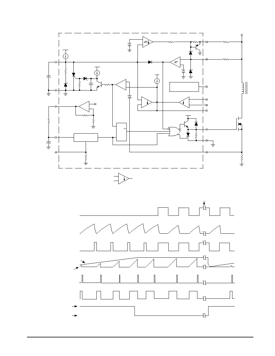
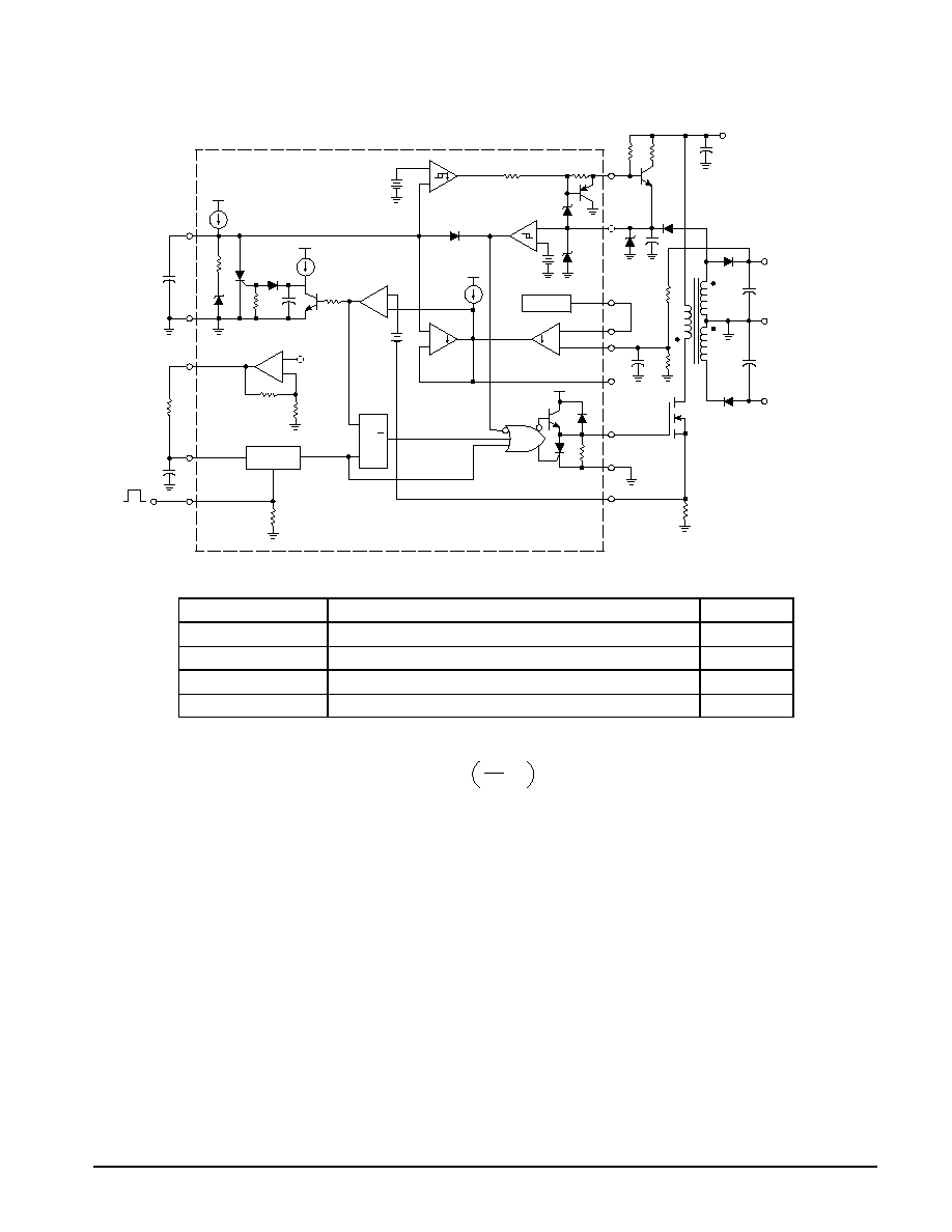
OPERATING DESCRIPTION
The MC34129 series are high performance current mode
switching regulator controllers specifically designed for use in
low power telecommunication applications. Implementation
will allow remote digital telephones and terminals to shed
their power cords and derive operating power directly from
the twisted pair used for data transmission. Although these
devices are primarily intended for use in digital telephone
systems, they can be used cost effectively in a wide range of
converter applications. A representative block diagram is
shown in Figure 18.
Oscillator
The oscillator frequency is programmed by the values
selected for the timing components RT and CT. Capacitor CT
is charged from the 2.5 V reference through resistor RT to
approximately 1.25 V and discharged by an internal current
sink to ground. During the discharge of CT, the oscillator
generates an internal blanking pulse that holds the lower
input of the NOR gate high. This causes the Drive Output to
be in a low state, thus producing a controlled amount of
output deadtime. Figure 1 shows Oscillator Frequency
versus RT and Figure 2 Output Deadtime versus Frequency,
both for given values of CT. Note that many values of RT and
CT will give the same oscillator frequency but only one
combination will yield a specific output deadtime at a give
frequency. In many noise sensitive applications it may be
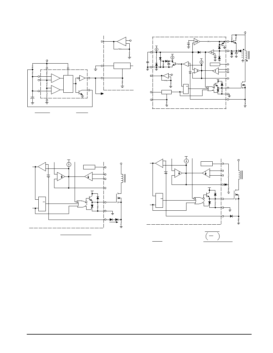
desirable to frequencylock one or more switching regulators
to an external system clock. This can be accomplished by
applying the clock signal to the Synch/Inhibit Input. For
reliable locking, the freerunning oscillator frequency should
be about 10% less than the clock frequency. Referring to the
timing diagram shown Figure 19, the rising edge of the clock
signal applied to the Sync/Inhibit Input, terminates charging
of CT and Drive Output conduction. By tailoring the clock
waveform, accurate duty cycle clamping of the Drive Output
can be achieved. A circuit method is shown in Figure 20. The
Sync/Inhibit Input may also be used as a means for system
shutdown by applying a dc voltage that is within the range of
2.0 V to VCC.
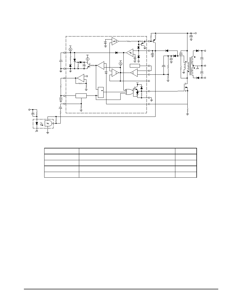
PWM Comparator and Latch
The MC34129 operates as a current mode controller
whereby output switch conduction is initiated by the oscillator
and terminated when the peak inductor current reaches a
threshold level established by the output of the Error Amp or
SoftStart Buffer (Pin 11). Thus the error signal controls the
peak inductor current on a cyclebycycle basis. The PWM
ComparatorLatch configuration used, ensures that only a
single pulse appears at the Drive Output during any given
oscillator cycle. The inductor current is converted to a voltage
by inserting the groundreferenced resistor RS in series with
the source of output switch Q1. The Ramp Input adds an
offset of 275 mV to this voltage to guarantee that no pulses
appear at the Drive Output when Pin 11 is at its lowest state.
This occurs at the beginning of the softstart interval or when
the power supply is operating and the load is removed. The
peak inductor current under normal operating conditions is
controlled by the voltage at Pin 11 where:
Ipk =
V(Pin 11) 0.275 V
RS
Abnormal operating conditions occur when the power
supply output is overloaded or if output voltage sensing is
lost. Under these conditions, the voltage at Pin 11 will be
internally clamped to 1.95 V by the output of the SoftStart
Buffer. Therefore the maximum peak switch current is:
Ipk(max) =
1.95 V 0.275
RS
RS
1.675 V
=
When designing a high power switching regulator it
becomes desirable to reduce the internal clamp voltage in
order to keep the power dissipation of RS to a reasonable
level. A simple method which adjusts this voltage in discrete
increments is shown in Figure 22. This method is possible
because the Ramp Input bias current is always negative
(typically 120
µ
A). A positive temperature coefficient equal
to that of the diode string will be exhibited by Ipk(max). An
adjustable method that is more precise and temperature
stable is shown in Figure 23. Erratic operation due to noise
pickup can result if there is an excessive reduction of the
clamp voltage. In this situation, high frequency circuit layout
techniques are imperative.
A narrow spike on the leading edge of the current
waveform can usually be observed and may cause the power
supply to exhibit an instability when the output is lightly
loaded. This spike is due to the power transformer
interwinding capacitance and output rectifier recovery time.
The addition of an RC filter on the Ramp Input with a time
constant that approximates the spike duration will usually
eliminate the instability; refer to Figure 25.
Error Amp and SoftStart Buffer
A fullycompensated Error Amplifier with access to both
inputs and output is provided for maximum design flexibility.
The Error Amplifier output is common with that of the
SoftStart Buffer. These outputs are opencollector (sink
only) and are ORed together at the inverting input of the PWM
Comparator. With this configuration, the amplifier that
demands lower peak inductor current dominates control of
the loop. SoftStart is mandatory for stable startup when
power is provided through a high source impedance such as
the long twisted pair used in telecommunications. It
effectively removes the load from the output of the switching
power supply upon initial startup. The SoftStart Buffer is
configured as a unity gain follower with the noninverting input
connected to Pin 12. An internal 1.0
µ
A current source
charges the softstart capacitor (CSoftStart) to an internally
clamped level of 1.95 V. The rate of change of peak inductor
current, during startup, is programmed by the capacitor value
selected. Either the Fault Timer or the Undervoltage Lockout
can discharge the softstart capacitor.
MC34129 MC33129
9
MOTOROLA ANALOG IC DEVICE DATA
Figure 18. Representative Block Diagram
Figure 19. Timing Diagram
+
+
+
+
+
+
+
+
+
Start/Run
Output
Vin = 20V
VCC
1.95V
Start/Run
Comparator
7.0V
13
12
1.0
µ
A
Fault Timer
Undervoltage
Lockout
14
VCC
VCC
CSoftStart
PWM
Comparator
VCC
80
µ
A
3.6V
14.3V
8
1.25V
Reference
2.5V Reference
275mV
9 Noninverting
Input
7
6
1.25V
Error Amp
10 Inverting
Input
R
SoftStart
Buffer
VCC
11
Feedback/PWM
Input
RT
R
Latch
Q1
1 Drive Output
5
Oscillator
R
Q
S
2
Drive
Gnd
CT
4
Sync/Inhibit Input
32k
3
Ramp Input
RS
=
Sink Only
Positive True Logic
35k
1.95V
225k
Sync/Inhibit Input
Capacitor CT
Latch
"Set" Input
Feedback/PWM Input
Ramp Input
Latch
"Reset" Input
Drive Output
Start/Run
Output
20 V
14.3 V
600
µ
s Delay

MC34129 MC33129
10
MOTOROLA ANALOG IC DEVICE DATA
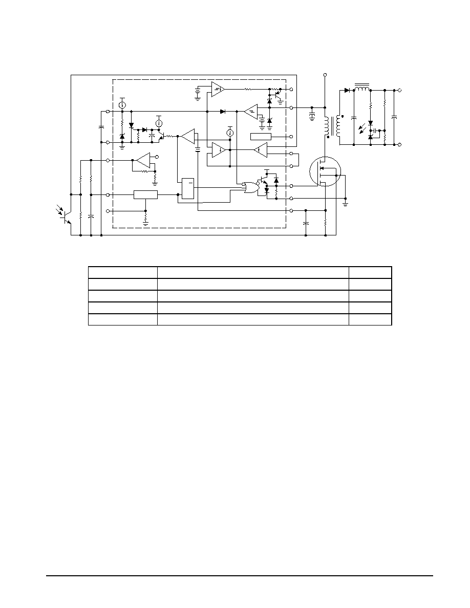
Fault Timer
This unique circuit prevents sustained operating in a
lockout condition. This can occur with conventional switching
control ICs when operating from a power source with a high
series impedance. If the power required by the load is greater
than that available from the source, the input voltage will
collapse, causing the lockout condition. The Fault Timer
provides automatic recovery when this condition is detected.
Under normal operating conditions, the output of the PWM
Comparator will reset the Latch and discharge the internal
Fault Timer capacitor on a cyclebycycle basis. Under
operating conditions where the required power into the load is
greater than that available from the source (Vin), the Ramp
Input voltage (plus offset) will not reach the comparator
threshold level (Pin 11), and the output of the PWM
Comparator will remain low. If this condition persists for more
that 600
µ
s, the Fault Timer will active, discharging CSoftStart
and initiating a softstart cycle. The power supply will operate
in a skip cycle or hiccup mode until either the load power or
source impedance is reduced. The minimum fault timeout is
200
µ
s, which limits the useful switching frequency to a
minimum of 5.0 kHz.
Start/Run Comparator
A bootstrap startup circuit is included to improve system
efficiency when operating from a high input voltage. The
output of the Start/Run Comparator controls the state of an
external transistor. A typical application is shown in Figure 21.
While CSoftStart is charging, startup bias is supplied to VCC
( P i n 1 4 ) f r o m Vin through transistor Q2. When
CSoftStart reaches the 1.95 V clamp level, the StartRun
output switches low (VCC = 50 mV), turning off Q2. Operating
bias is now derived from the auxiliary bootstrap winding of the
transformer, and all drive power is efficiently converted down
from Vin. The start time must be long enough for the power
supply output to reach regulation. This will ensure that there
is sufficient bias voltage at the auxiliary bootstrap winding for
sustained operation.
tStart =
1.95 V CSoftStart
1.0
µ
A
= 1.95 CSoftStart in
µ
F
The Start/Run Comparator has 350 mV of hysteresis. The
output offstate is clamped to VCC + 7.6 V by the internal
zener and PNP transistor baseemitter junction.
Drive Output and Drive Ground
The MC34129 contains a single totempole output stage
that was specifically designed for direct drive of power
MOSFETs. It is capable of up to
±
1.0 A peak drive current and
has a typical fall time of 30 ns with a 500 pF load. The
totempole stage consists of an NPN transistor for turnon
drive and a high speed SCR for turnoff. The SCR design
requires less average supply current (ICC) when compared to
conventional switching control ICs that use an all NPN
totempole. The SCR accomplishes this during turnoff of
the MOSFET, by utilizing the gate charge as regenerative
onbias, whereas the conventional all transistor design
requires continuous base current. Conversion efficiency in
low power applications is greatly enhanced with this
reduction of ICC. The SCR's lowstate holding current (IH) is
typically 225
µ
A. An internal 225 k
pulldown resistor is
included to shunt the Drive Output offstate leakage to
ground when the Undervoltage Lockout is active. A separate
Drive Ground is provided to reduce the effects of switching
transient noise imposed on the Ramp Input. This feature
becomes particularly useful when the Ipk(max) clamp level is
reduced. Figure 24 shows the proper implementation of the
MC34129 with a current sensing power MOSFET.
Undervoltage Lockout
The Undervoltage Lockout comparator holds the Drive
Output and CSoftStart pins in the low state when VCC is less
than 3.6 V. This ensures that the MC34129 is fully functional
before the output stage is enabled and a softstart cycle
begins. A builtin hysteresis of 350 mV prevents erratic
output behavior as VCC crosses the comparator threshold
voltage. A 14.3 V zener is connected as a shunt regulator
from VCC to ground. Its purpose is to protect the MOSFET
gate from excessive drove voltage during system startup. An
external 9.1 V zener is required when driving low threshold
MOSFETs. Refer to Figure 21. The minimum operating
voltage range of the IC is 4.2 V to 12 V.
References
The 1.25 V bandgap reference is trimmed to
±
2.0%
tolerance at TA = 25
°
C. It is intended to be used in
conjunction with the Error Amp. The 2.50 V reference is
derived from the 1.25 V reference by an internal op amp with
a fixed gain of 2.0. It has an output tolerance of
±
5.0% at TA =
25
°
C and its primary purpose is to supply charging current to
the oscillator timing capacitor.
For further information, please refer to AN976.
MC34129 MC33129
11
MOTOROLA ANALOG IC DEVICE DATA
Figure 20. External Duty Cycle Clamp
and MultiUnit Synchronization
Figure 21. Bootstrap Startup
Figure 22. Discrete Step Reduction of Clamp Level
Figure 23. Adjustable Reduction of Clamp Level
The external 9.1 V zener is required when driving low threshold MOSFETs.
CSoftStart
12
7
6
5
4
2.5V
OSC
R
S
Q
1.25V
13
14
9.1
V
8
9
10
11
1
2
3
Q2
Vin
+
+
+
+
+
+
+
Ipk(max) =
1.675 (VF(D1) + VF(D2))
275mV
R
S
Q
1.25V
8
9
10
11
1
2
3
Vin
Q1
RS
D1
D2
120
µ
A
+
+
+
RS
275mV
R
S
Q
1.25V
8
9
10
11
1
2
3
Vin
Q1
RS
R1
R2
+
+
+
If:
1.25 V
R1 + R2
1.0 mA
Then: Ipk(max)
1.25
R2
R1
+ 1
0.275
RS
f =
1.44
(RA + 2RB)C
Dmax =
RB
5.0V
RA
RB
8
6
5
2
C
5.0k
4
R
Q
S
MC1455
3
7
6
5
4
2.5V
OSC
To Additional
MC34129's
+
5.0k
5.0k
1
+
+
RA + 2RB
MC34129 MC33129
12
MOTOROLA ANALOG IC DEVICE DATA
Figure 24. Current Sensing Power MOSFET
Figure 25. Current Waveform Spike Suppression
Figure 26. MOSFET Parasitic Oscillations
Figure 27. Bipolar Transistor Drive
VRS
RS
Ipk
rDS(on)
If: SENSEFET = MTP10N10M
RS = 200
Then: VRS
0.075 Ipk
1.25V
8
9
10
11
1
2
3
Vin
D
SENSEFET
G
M
K
S
Power Ground:
To Input Source
Return
RS
1/4W
Control Circuitry Ground:
To Pin 7
Virtually lossless current sensing can be achieved with the implementation of a
SENSEFET power switch.
+
rDM(on) + rS
The addition of the RC filter will eliminate instability caused by the
leading edge spike on the current waveform.
1
2
3
Vin
Q1
R
C
RS
1
2
3
Vin
Q1
RS
Rg
Series gate resistor Rg will damp any high frequency parasitic
oscillations caused by the MOSFET input capacitance and any
series wiring inductance in the gatesource circuit.
The totempole output can furnish negative base current for enhanced
transistor turnoff, with the addition of capacitor C1.
1
2
3
Vin
Q1
RS
C1
IB
+
0
Base Charge
Removal
t
MC34129 MC33129
13
MOTOROLA ANALOG IC DEVICE DATA
Figure 28. NonIsolated 725 mW Flyback Regulator
T1: Coilcraft #G6807A
Primary = 90T #28 AWG
Secondary
±
5V = 26T #30 AW
Gap = 0.05 n, for Lp of 600
µ
H
Core = Ferroxcube 813E1873C8
Bobbin = Ferroxcube E187PCB18
12
0.1
7
24k
470pF
128kHz
Sync
6
5
4
2.5 V
OSC
R
S
Q
1.25V
220k
13
14
1N958A
8
9
10
500pF
11
1
2
3
2.2k
2N5551
1N4148
+ 10
36k
R2
12k
R1
MTP
2N20L
10
50
T1
1N5819
5V/125mA
100
Gnd
100
5V/20mA
1N5819
Vin = 20V to 48V
+
+
+
+
+
+
+
+
+
Test
Conditions
Results
Line Regulation 5.0 V
Vin = 20 V to 40 V, Iout 5.0 V = 125 mA, Iout 5.0 V = 20 mA
= 1.0 mV
Load Regulation 5.0 V
Vin = 30 V, Iout 5.0 V = 0 mA to 150 mA, Iout 5.0 V = 20 mA
= 2.0 mV
Output Ripple 5.0 V
Vin = 30 V, Iout 5.0 V = 125 mA, Iout 5.0 V = 20 mA
150 mVpp
Efficiency
Vin = 30 V, Iout 5.0 V = 125 mA, Iout 5.0 V = 20 mA
77%
Vout = 1.25
R2
R1
+ 1
MC34129 MC33129
14
MOTOROLA ANALOG IC DEVICE DATA
Figure 29. Isolated 2.0 W Flyback Regulator
T1: Primary = 35T #32 AWG
Feedback = 12T #32 AWG
Secondary
±
5 V = 7T #32 AWG
Gap = 0.004
, for Lp of 180
µ
H
Core = Ferroxcube 813E1873C8
Bobbin = Ferroxcube E187PCB18
12
0.1
7
24k
470pF
6
5
4
2.5V
OSC
R
S
Q
1.25V
220k
13
14
8
9
10
11
1
2
Gnd
5V/20mA
Vin = 20V to 48V
0.1
2.7k
1
2
6
5
4
10k
128kHz
Sync
MOC5007
2.2k
2N5551
100
1N5819
180
pF
2
0.1
140k
330
20k
T1
1N5819
5V/380mA
100
100
1N5819
MTP
2N20
100pF
100
+
+
+
+
+
+
+
1N5819
+
+
+
3
Test
Conditions
Results
Line Regulation 5.0 V
Vin = 20 V to 40 V, Iout 5.0 V = 380 mA, Iout 5.0 V = 20 mA
= 1.0 mV
Load Regulation 5.0 V
Vin = 30 V, Iout 5.0 V = 100 mA to 380 mA, Iout 5.0 V = 20 mA
= 15 mV
Output Ripple 5.0 V
Vin = 30 V, Iout 5.0 V = 380 mA, Iout 5.0 V = 20 mA
150 mVpp
Efficiency
Vin = 30 V, Iout 5.0 V = 380 mA, Iout 5.0 V = 20 mA
73%
MC34129 MC33129
15
MOTOROLA ANALOG IC DEVICE DATA
Figure 30. Isolated 3.0 W Flyback Regulator with Secondary Side Sensing
T1:
L1:
Primary = 22T #18 AWG
Secondary = 22T #18 AWG
Lp = 50
µ
H
Core = Ferroxcube
2616PA1003C8
Bobbin = Ferroxcube 2616F1D
Coilcraft Z7156, 15
µ
H
12
0.1
7
6
5
4
2.5V
OSC
R
S
Q
1.25V
13
14
8
9
10
11
1
2
3
Vin = 12V
D
G
M
K
S
1N5821
L1
5/60mA
470
1/2
4N26
51
100
0.1
Return
TL431A
MTP10N10M
1/2
4N26
+
+
+
+
+
2.2k
15k
510
0.002
+
+
3.9k
3.9k
200
0.001
100
Test
Conditions
Results
Line Regulation
Vin = 8.0 V to 12 V, Iout 600 mA
= 1.0 mV
Load Regulation
Vin = 12 V, Iout = 100 mA to 600 mA
= 8.0 mV
Output Ripple
Vin = 12 V, Iout = 600 mA
20 mVpp
Efficiency
Vin = 12 V, Iout = 600 mA
81%
An economical method of achieving secondary sensing is to combine the TL431A with a 4N26 optocoupler.
MC34129 MC33129
16
MOTOROLA ANALOG IC DEVICE DATA
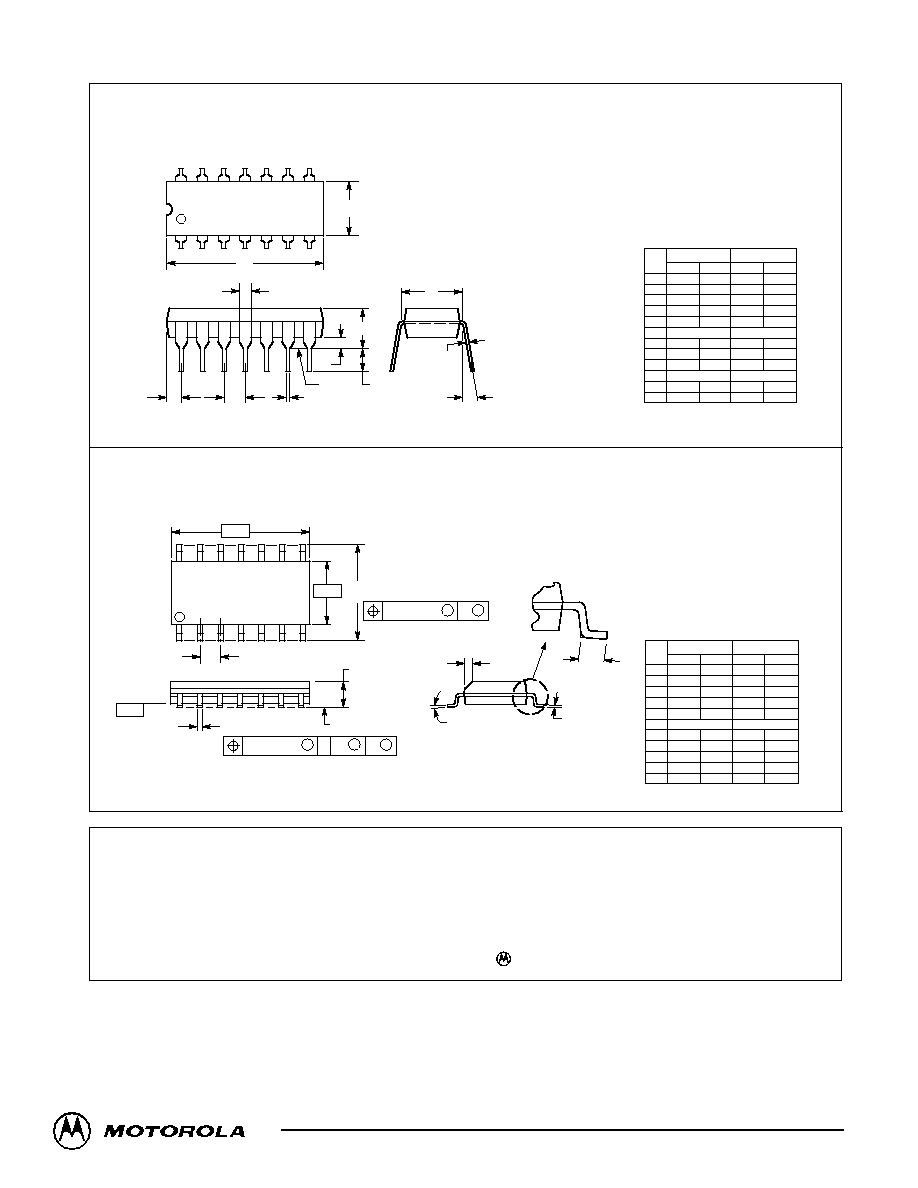
OUTLINE DIMENSIONS
P SUFFIX
PLASTIC PACKAGE
CASE 64606
ISSUE L
D SUFFIX
PLASTIC PACKAGE
CASE 751A03
(SO14)
ISSUE F
NOTES:
1. LEADS WITHIN 0.13 (0.005) RADIUS OF TRUE
POSITION AT SEATING PLANE AT MAXIMUM
MATERIAL CONDITION.
2. DIMENSION L TO CENTER OF LEADS WHEN
FORMED PARALLEL.
3. DIMENSION B DOES NOT INCLUDE MOLD
FLASH.
4. ROUNDED CORNERS OPTIONAL.
1
7
14
8
B
A
F
H
G
D
K
C
N
L
J
M
SEATING
PLANE
DIM
MIN
MAX
MIN
MAX
MILLIMETERS
INCHES
A
0.715
0.770
18.16
19.56
B
0.240
0.260
6.10
6.60
C
0.145
0.185
3.69
4.69
D
0.015
0.021
0.38
0.53
F
0.040
0.070
1.02
1.78
G
0.100 BSC
2.54 BSC
H
0.052
0.095
1.32
2.41
J
0.008
0.015
0.20
0.38
K
0.115
0.135
2.92
3.43
L
0.300 BSC
7.62 BSC
M
0
10 0 10
N
0.015
0.039
0.39
1.01
_
_
_
_
NOTES:
1. DIMENSIONING AND TOLERANCING PER
ANSI Y14.5M, 1982.
2. CONTROLLING DIMENSION: MILLIMETER.
3. DIMENSIONS A AND B DO NOT INCLUDE
MOLD PROTRUSION.
4. MAXIMUM MOLD PROTRUSION 0.15 (0.006)
PER SIDE.
5. DIMENSION D DOES NOT INCLUDE DAMBAR
PROTRUSION. ALLOWABLE DAMBAR
PROTRUSION SHALL BE 0.127 (0.005) TOTAL
IN EXCESS OF THE D DIMENSION AT
MAXIMUM MATERIAL CONDITION.
A
B
G
P
7 PL
14
8
7
1
M
0.25 (0.010)
B
M
S
B
M
0.25 (0.010)
A
S
T
T
F
R
X 45
SEATING
PLANE
D
14 PL
K
C
J
M
_
DIM
MIN
MAX
MIN
MAX
INCHES
MILLIMETERS
A
8.55
8.75
0.337
0.344
B
3.80
4.00
0.150
0.157
C
1.35
1.75
0.054
0.068
D
0.35
0.49
0.014
0.019
F
0.40
1.25
0.016
0.049
G
1.27 BSC
0.050 BSC
J
0.19
0.25
0.008
0.009
K
0.10
0.25
0.004
0.009
M
0
7
0
7
P
5.80
6.20
0.228
0.244
R
0.25
0.50
0.010
0.019
_
_
_
_
Motorola reserves the right to make changes without further notice to any products herein. Motorola makes no warranty, representation or guarantee regarding
the suitability of its products for any particular purpose, nor does Motorola assume any liability arising out of the application or use of any product or circuit, and
specifically disclaims any and all liability, including without limitation consequential or incidental damages. "Typical" parameters which may be provided in Motorola
data sheets and/or specifications can and do vary in different applications and actual performance may vary over time. All operating parameters, including "Typicals"
must be validated for each customer application by customer's technical experts. Motorola does not convey any license under its patent rights nor the rights of
others. Motorola products are not designed, intended, or authorized for use as components in systems intended for surgical implant into the body, or other
applications intended to support or sustain life, or for any other application in which the failure of the Motorola product could create a situation where personal injury
or death may occur. Should Buyer purchase or use Motorola products for any such unintended or unauthorized application, Buyer shall indemnify and hold Motorola
and its officers, employees, subsidiaries, affiliates, and distributors harmless against all claims, costs, damages, and expenses, and reasonable attorney fees
arising out of, directly or indirectly, any claim of personal injury or death associated with such unintended or unauthorized use, even if such claim alleges that Motorola
was negligent regarding the design or manufacture of the part. Motorola and are registered trademarks of Motorola, Inc. Motorola, Inc. is an Equal
Opportunity/Affirmative Action Employer.
How to reach us:
USA / EUROPE / Locations Not Listed: Motorola Literature Distribution;
JAPAN: Nippon Motorola Ltd.; TatsumiSPDJLDC, 6F SeibuButsuryuCenter,
P.O. Box 20912; Phoenix, Arizona 85036. 18004412447 or 6023035454
3142 Tatsumi KotoKu, Tokyo 135, Japan. 038135218315
MFAX: RMFAX0@email.sps.mot.com TOUCHTONE 6022446609
ASIA/PACIFIC: Motorola Semiconductors H.K. Ltd.; 8B Tai Ping Industrial Park,
INTERNET: http://DesignNET.com
51 Ting Kok Road, Tai Po, N.T., Hong Kong. 85226629298
MC34129/D
*MC34129/D*