
Order this document by MC33218A/D
Device
Operating
Temperature Range
Package
MC33218A
SEMICONDUCTOR
TECHNICAL DATA
DW SUFFIX
PLASTIC PACKAGE
CASE 751E
VOICE SWITCHED
SPEAKERPHONE WITH
µ
PROCESSOR INTERFACE
PIN CONNECTIONS
ORDERING INFORMATION
MC33218ADW
MC33218AP
TA = 40
°
to +85
°
C
SO24L
Plastic DIP
24
1
P SUFFIX
PLASTIC PACKAGE
CASE 724
24
1
CP2
1
24
(Top View)
VCC
2
3
4
5
6
7
8
9
10
11
12
23
22
21
20
19
18
17
16
15
14
13
XDI
CPT
TLI
TLO
VB
CT
CD
NC
CPR
RLI
RLO
TAO
MCO
MCI
POR
DR
DATA
CLK
RXI
RXO
RAO
GND
1
MOTOROLA ANALOG IC DEVICE DATA
Advance Information
Voice Switched Speakerphone
with Microprocessor Interface
The Motorola MC33218A Voice Switched Speakerphone Circuit
incorporates the necessary amplifiers, attenuators, level detectors, and
control algorithm to form the heart of a high quality handsfree
speakerphone system. Included are a microphone amplifier with mute,
transmit and receive attenuators, a background monitoring system for both
the transmit and receive paths, and level detectors for each path. An AGC
system reduces the receive gain on long lines where loop current and power
are in short supply. A dial tone detector prevents fading of dial tone. A Chip
Disable pin permits conserving power when the circuit is not in use.
Additionally, the MC33218A has a serial data port which permits
microprocessor control of the receive volume level, microphone mute,
attenuator range, and selection of transmit, receive, idle or normal modes.
The data port can be operated at up to 1.0 MHz.
The MC33218A can be operated from a power supply, or from the
telephone line, requiring typically 4.6 mA. It can be used in conjunction with a
variety of speech networks. Applications include not only speakerphones,
but intercoms and other voice switched devices.
·
Supply Voltage Range: 2.7 to 6.5 V
·
Attenuator Range: 53 or 27 dB (Selectable)
·
2 Point Sensing with Background Noise Monitor in Each Path
·
Microprocessor Port for Control of:
Volume Control (40 dB Range over 16 Levels)
Mute Microphone Amplifier
Force to Receive, Transmit, or Idle Modes
Attenuator Range Selection (27 or 53 dB)
·
Chip Disable Pin Powers Down the Entire IC
·
24 Pin Narrow Body (300 mil) DIP and 24 Pin SOIC
This document contains information on a new product. Specifications and information herein are
subject to change without notice.
©
Motorola, Inc. 1995
Simplified Block Diagram
This device contains 610 active transistors.
Microphone
Transmit
Out
VB
VB
VB
VB
VB
BNM
Reg.
Rx Attenuator
MC33218A
VCC
Tx Attenuator
Attenuator Control
DTD
Speaker
Amplifier
Speaker
CD
Receive
In
BNM
DR
DATA
POR
CLK
Serial
Port

MC33218A
2
MOTOROLA ANALOG IC DEVICE DATA
MAXIMUM RATINGS
Rating
Symbol
Min
Max
Unit
Supply Voltage
VCC
0.5
7.0
Vdc
Any Input
Vin
0.4
VCC + 0.4
Vdc
Maximum Junction Temperature
TJ
+150
°
C
Storage Temperature Range
Tstg
65
+150
°
C
NOTE: Devices should not be operated at or outside these values. The "Recommended Operating Limits"
provide for actual device operation.
RECOMMENDED OPERATING LIMITS
Characteristic
Symbol
Min
Typ
Max
Unit
Supply Voltage (NonAGC Range)
VCC
3.5
6.5
Vdc
(AGC Range)
2.7
3.5
Maximum Attenuator Input Signal
Vin(max)
300
mVrms
Logic Input Voltage (Pins 8, 1719)
VINL
Vdc
Low
0
0.8
High
2.0
VCC
Clock and Data Rate (Serial Port)
FDATA
0
1.0
MHz
VB Output Current
IVB
See
Figure 14
mA
Operating Ambient Temperature Range
TA
40
+85
°
C
ELECTRICAL CHARACTERISTICS
(TA = + 25
°
C, VCC = 5.0 V, CD
0.8 V, unless noted, see Figure 3.)
Characteristic
Symbol
Min
Typ
Max
Unit
POWER SUPPLY
Supply Current (Enabled, CD
0.8, VB Open, See Figure 13)
ICCE
mA
Idle Mode
3.0
4.6
6.0
Tx Mode
4.6
Rx Mode
5.3
Supply Current (Disabled, CD = 2.0 V, VB Open)
ICCD
µ
A
VCC = 3.0 V
67
VCC = 5.0 V
50
110
170
VCC = 6.5 V
150
VB Output Voltage (IVB = 0, CD = 0)
VB
Vdc
VCC = 2.7 V
0.9
VCC = 5.0 V
2.1
2.2
2.3
VCC = 6.5 V
3.0
VB Output Resistance (IVB
1.0 mA)
ROVB
600
PSRR @ VB versus VCC, f = 1.0 KHz, CVB = 100
µ
F
PSRR
57
dB
ATTENUATOR CONTROL
CT Voltage (with Respect to VB)
VCT VB
mV
(Full Range, B5 = 0) Rx Mode (Maximum Volume)
+150
(Full Range, B5 = 0)
Idle Mode
0
(Full Range, B5 = 0)
Tx Mode
100
(Half Range, B5 = 1) Rx Mode (Maximum Volume
+85
(Half Range, B5 = 1)
Idle Mode
0
(Half Range, B5 = 1)
Tx Mode
35
CT Source Current (Switching to Rx Mode)
ICTR
55
42
33
µ
A
CT Sink Current (Switching to Tx Mode)
ICTT
33
42
55
µ
A
CT Idle Current
ICTI
3.0
0
3.0
µ
A
Dial Tone Detector Threshold (with Respect to VB at RXO)
VDT
40
20
8.0
mV

MC33218A
3
MOTOROLA ANALOG IC DEVICE DATA
ELECTRICAL CHARACTERISTICS (continued)
(TA = + 25
°
C, VCC = 5.0 V, CD
0.8 V, unless noted, see Figure 3.)
Characteristic
Unit
Max
Typ
Min
Symbol
ATTENUATORS
Receive Attenuator Gain (f = 1.0 kHz, Maximum Volume)
dB
Full Attenuation Range (B5 = 0)
Rx Mode
GRXF
3.0
6.7
9.0
Tx Mode
GRXTF
49
47
43
Idle Mode
GRXIF
28
25
22
Range (Rx to Tx Mode)
GRXF
50
53
56
Half Attenuation Range (B5 = 1)
Rx Mode
GRXH
10
7.0
4.0
Tx Mode
GRXTH
37
34
31
Idle Mode
GRXIH
28
25
22
Range (Rx to Tx Mode)
GRXH
23
27
29
Volume Control Range
(Rx Mode Only, B3B0 Changed from 0000 to 1111, See Figures 6, 7)
VCR
dB
Full Range
34
40
46
Half Range
25
AGC Attenuation Range
(VCC = 3.5 to 2.7 V, Receive Mode Only, B3B0 = 0000, See Figure 8)
GAGC
dB
Full Range
12
21
28
Half Range
19
Transmit Attenuator Gain (f = 1.0 kHz, Maximum Volume)
dB
Full Attenuation Range (B5 = 0)
Tx Mode
GTXF
3.0
6.7
9.0
Rx Mode
GTXRF
49
47
43
Idle Mode
GTXIF
19
16
13
Range (Tx to Rx Mode)
GTXF
50
53
56
Half Attenuation Range (B5 = 1)
Tx Mode
GTXH
9.0
6.5
3.0
Rx Mode
GTXRH
36
34
30
Idle Mode
GTXIH
19
16
13
Range (Tx to Rx Mode)
GTXH
23
27
29
RAO, TAO Output Current Capability
IOATT
2.0
mA
RAO Offset Voltage with Respect to VB
VRAO
mVdc
Rx Mode
50
Idle Mode
0
Tx Mode
2.0
TAO Offset Voltage with Respect to VB
VTAO
mVdc
Rx Mode
2.0
Idle Mode
5.0
Tx Mode
50
MICROPHONE AMPLIFIER (Pins 21, 22)
Output Offset with Respect to VB (RF = 300 k
)
MCOVOS
10
mVdc
Input Bias Current (Pin 21)
IMBIAS
30
nA
Open Loop Gain (f < 100 Hz)
AVOLM
80
dB
Gain Bandwidth
GBWM
1.5
MHz
Maximum Output Voltage Swing (Note 1)
VOMAX
350
mVrms
Maximum Output Current Capability
IOMCO
2.0
mA
MUTING (
Gain)
Microphone Amplifier Only (Measured at Pin 22)
AMT
dB
RF = 300 k
73
RF = 100 k
64
Microphone Amplifier + Transmit Attenuator in Receive Mode
(Measured at Pin 23) RF = 300 k
TMT
95
113
dB
NOTE: 1. Output swing is limited by the capability of the transmit attenuator input. See Figure 16.

MC33218A
4
MOTOROLA ANALOG IC DEVICE DATA
ELECTRICAL CHARACTERISTICS (continued)
(TA = + 25
°
C, VCC = 5.0 V, CD
0.8 V, unless noted, see Figure 3.)
Characteristic
Unit
Max
Typ
Min
Symbol
MUTING (
Gain)
Timing from Data Ready LotoHi (See Figure 27)
µ
s
To Mute
tMM
2.0
To Enable
tENM
1.0
RECEIVE AMPLIFIER (Pins 15, 16)
Output Offset with Respect to VB (RF = 10 k
)
RXOVOS
1.3
mVdc
Input Bias Current (Pin 16)
IRBIAS
30
nA
Open Loop Gain (f < 100 Hz)
AVOLR
80
dB
Gain Bandwidth
GBWR
1.5
MHz
Maximum Output Voltage Swing (Note 2)
VOMAX
350
mVrms
Maximum Output Current Capability
IORXO
2.0
mA
LEVEL DETECTORS AND BACKGROUND NOISE MONITORS
TxRx Switching Threshold (Pins 4, 11)
ITH
0.8
1.0
1.2
µ
A/
µ
A
CPR, CPT Output Resistance (for Pulldown)
RCP
5.0
CPR, CPT Leakage Current
ICPLK
0.2
µ
A
CPR, CPT Nominal DC Voltage (No Signal)
VCP
1.9
Vdc
TLO, RLO, CP2 Source Current (@ VB 1.0 V)
ILDOH
2.0
mA
TLO, RLO, CP2 Output Resistance
RLD
500
TLO, RLO, CP2 Sink Current (@ VB + 1.0 V)
ILDOL
2.0
µ
A
CD INPUT (Pin 8)
Switching Threshold
VTHCD
1.5
Vdc
Input Resistance (Vin = 0.8 V)
RCD
170
235
300
k
Input Current (Vin = 5.0 V)
ICD
40
µ
A
Timing
µ
s
To Disable
tCD
3.0
To Enable
tENC
See
Figure 26
POR INPUT (Pin 20)
Switching Threshold (2.7 V
VCC
6.5 V)
VTHPOR
1.2
Vdc
Nominal DC Voltage (2.7 V
VCC
6.5 V)
VPOR
1.5
Vdc
Effective Resistance (0 V < Vin < 0.5 V)
RPOR
70
115
160
k
Input Current
IPOR
µ
A
Vin = 0 V
40
Vin = 5.0 V
630
Timing to Reset (Pin 20 Taken to < 1.2 V)
tPOR
30
µ
s
Minimum Power On Reset Time (See Figure 20)
TMPOR
ms
C = 0.1
µ
F VCC = 6.5 V
2.7
C = 0.1
µ
F
VCC = 5.0 V
3.7
C = 0.1
µ
F
VCC = 2.7 V
10.6
NOTE: 2. Output swing is limited by the capability of the receive attenuator input. See Figure 16.
MC33218A
5
MOTOROLA ANALOG IC DEVICE DATA
ELECTRICAL CHARACTERISTICS (continued)
(TA = + 25
°
C, VCC = 5.0 V, CD
0.8 V, unless noted, see Figure 3.)
Characteristic
Unit
Max
Typ
Min
Symbol
SERIAL PORT (Pins 1719)
Switching Threshold
VTHSP
1.3
Vdc
Clock Input Current (Pin 17)
IINCK
µ
A
DR
0.8 V Vin = 0.9 V
5.6
7.5
12.8
DR
0.8 V
Vin = 5.0 V
75
DR
2.0 V Vin = 0.6 V
5.2
7.9
13.3
DR
2.0 V
Vin = 5.0 V
84
Data Input Current (Pin 18)
Vin = 0.9 V
Vin = 5.0 V
IINDA
5.6
7.5
75
12.8
µ
A
Data Ready Input Current (Pin 19)
Vin = 0.9 V
Vin = 5.0 V
IINDR
13.8
20
200
36
µ
A
Timing (Minimum Requirements) (See Figure 2)
ns
Data Ready Falling Edge to Clock
t1
200
8th Clock Rising Edge to DR Rising Edge
t2
100
Data Setup Time
t3
100
Data Hold Time
t4
100
Clock High Time
t5
200
SYSTEM DISTORTION (See Figure 1)
Microphone Amplifier + Tx Attenuator Distortion
THDT
0.2
3.0
%
Receive Amplifier + Rx Attenuator Distortion
THDR
0.2
3.0
%
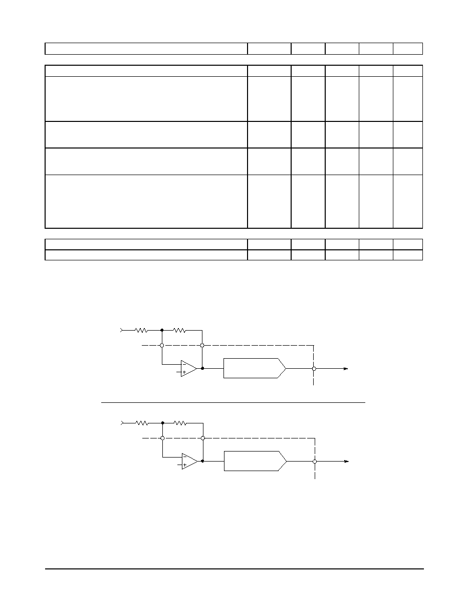
Figure 1. System Distortion Test
Vout
Vin
3.5 mV
1.0 kHz
VB
Tx Attenuator
23
TAO
22
21
MCI
MCO
3.0 k
300 k
NOTE: Rx Attenuator forced to receive mode.
NOTE: Tx Attenuator forced to transmit mode.
Vout
Vin
350 mV
1.0 kHz
VB
Rx Attenuator
14
RAO
15
16
RXI
RXO
10 k
10 k