Device
Operating
Temperature Range
Package
MC1496, B
SEMICONDUCTOR
TECHNICAL DATA
BALANCED
MODULATORS/DEMODULATORS
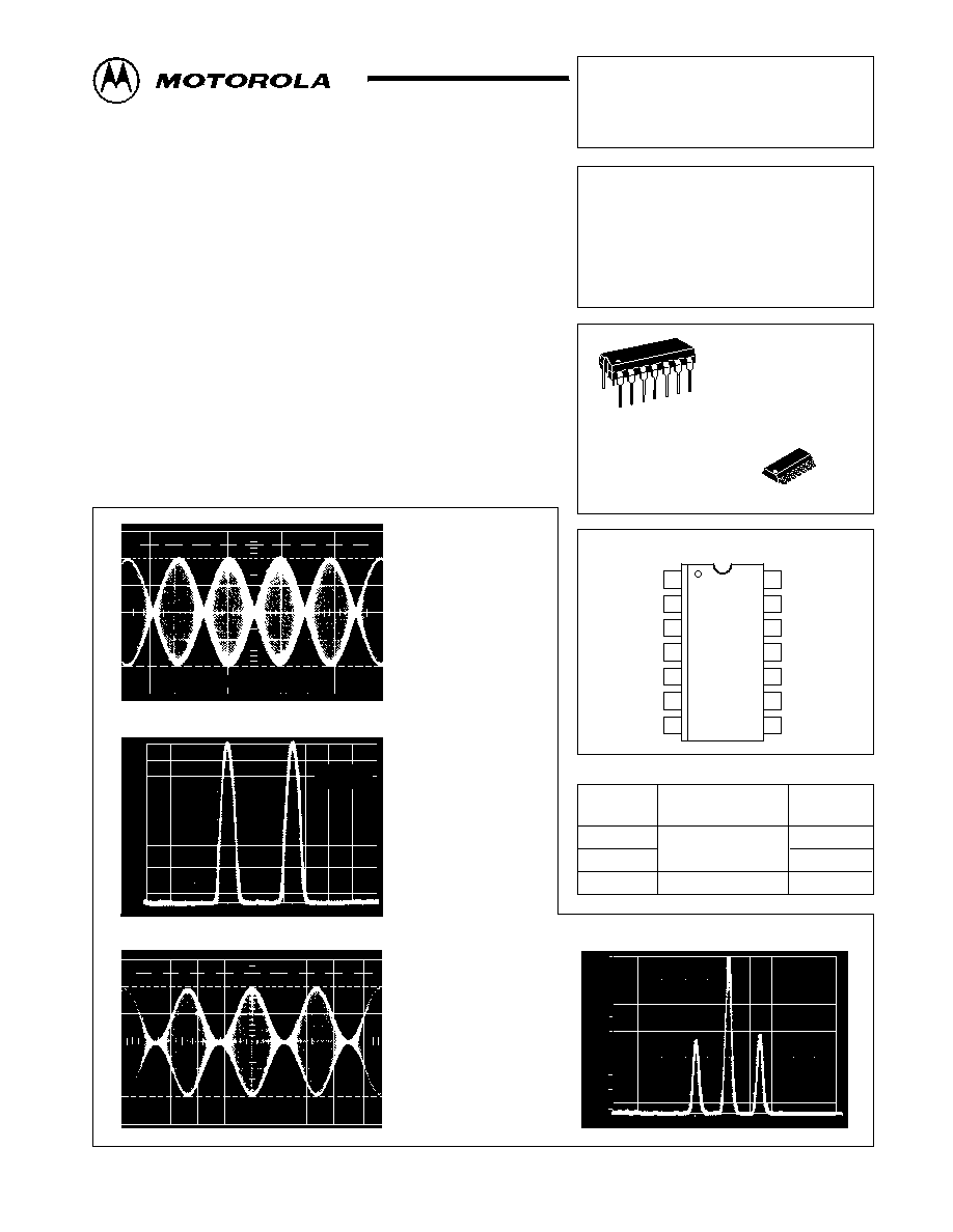
ORDERING INFORMATION
MC1496D
MC1496P
TA = 0
°
C to +70
°
C
SO14
Plastic DIP
PIN CONNECTIONS
Order this document by MC1496/D
D SUFFIX
PLASTIC PACKAGE
CASE 751A
(SO14)
P SUFFIX
PLASTIC PACKAGE
CASE 646
Signal Input
1
2
3
4
5
6
7
10
11
14
13
12
9
N/C
Output
Bias
Signal Input
Gain Adjust
Gain Adjust
Input Carrier
8
VEE
N/C
Output
N/C
Carrier Input
N/C
14
1
14
1
MC1496BP
Plastic DIP
TA = 40
°
C to +125
°
C
1
MOTOROLA ANALOG IC DEVICE DATA
Balanced Modulators/
Demodulators
These devices were designed for use where the output voltage is a
product of an input voltage (signal) and a switching function (carrier). Typical
applications include suppressed carrier and amplitude modulation,
synchronous detection, FM detection, phase detection, and chopper
applications. See Motorola Application Note AN531 for additional design
information.
·
Excellent Carrier Suppression 65 dB typ @ 0.5 MHz
Excellent Carrier Suppression
50 dB typ @ 10 MHz
·
Adjustable Gain and Signal Handling
·
Balanced Inputs and Outputs
·
High Common Mode Rejection 85 dB typical
This device contains 8 active transistors.
Figure 1. Suppressed
Carrier Output
Waveform
Figure 2. Suppressed
Carrier Spectrum
Figure 3. Amplitude
Modulation Output
Waveform
Figure 4. AmplitudeModulation Spectrum
IC = 500 kHz, IS = 1.0 kHz
IC = 500 kHz
IS = 1.0 kHz
60
40
20
0
Log Scale Id
499 kHz
500 kHz
501 kHz
IC = 500 kHz
IS = 1.0 kHz
IC = 500 kHz
IS = 1.0 kHz
499 kHz
500 kHz
501 kHz
Linear Scale
10
8.0
6.0
4.0
2.0
0
©
Motorola, Inc. 1996
Rev 4
MC1496, B
2
MOTOROLA ANALOG IC DEVICE DATA
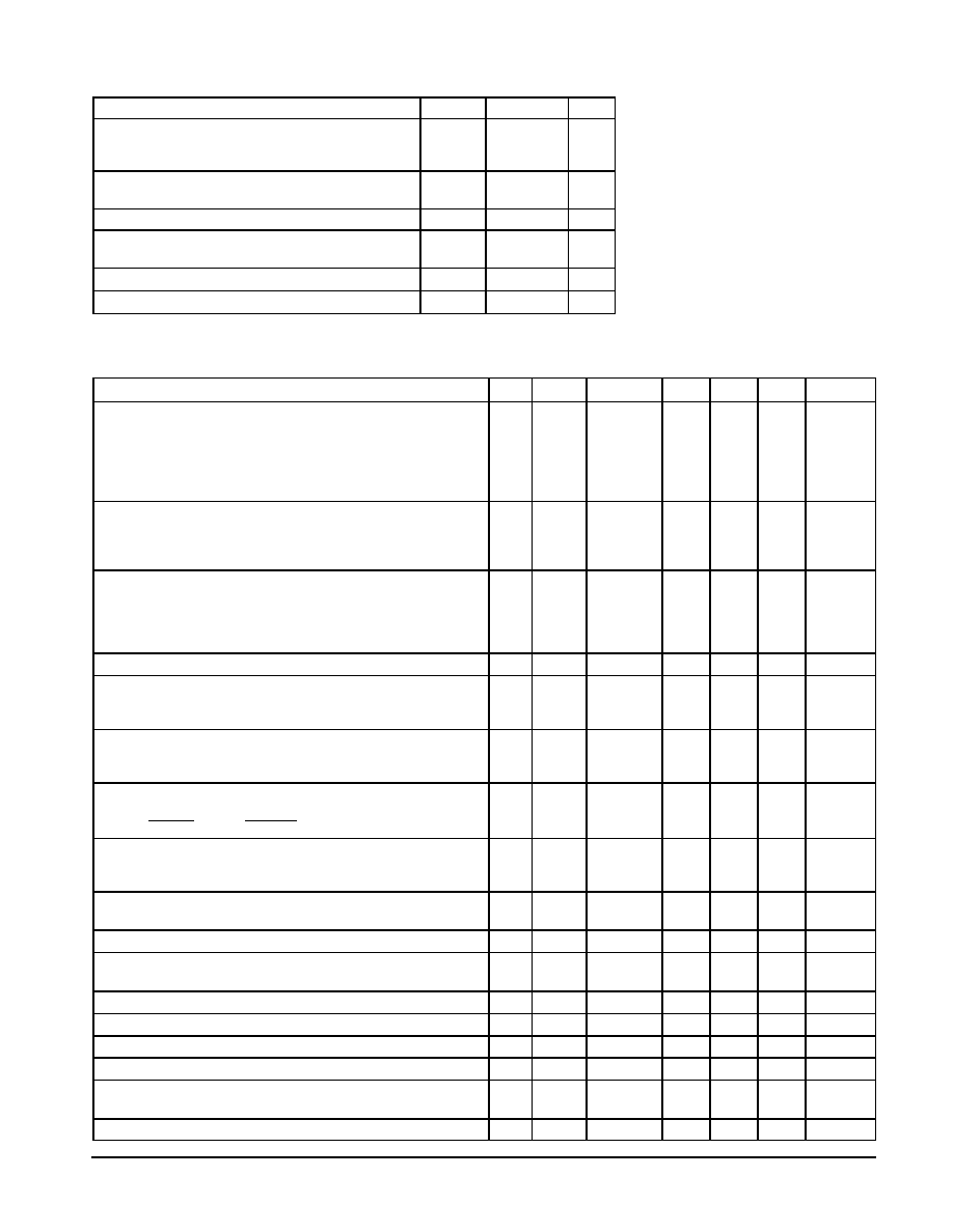
MAXIMUM RATINGS
(TA = 25
°
C, unless otherwise noted.)
Rating
Symbol
Value
Unit
Applied Voltage
(V6 V8, V10 V1, V12 V8, V12 V10, V8 V4,
V8 V1, V10 V4, V6 V10, V2 V5, V3 V5)
V
30
Vdc
Differential Input Signal
V8 V10
V4 V1
+5.0
±
(5 + I5Re)
Vdc
Maximum Bias Current
I5
10
mA
Thermal Resistance, JunctiontoAir
Plastic Dual InLine Package
R
JA
100
°
C/W
Operating Temperature Range
TA
0 to +70
°
C
Storage Temperature Range
Tstg
65 to +150
°
C
NOTE:
ESD data available upon request.
ELECTRICAL CHARACTERISTICS
(VCC = 12 Vdc, VEE = 8.0 Vdc, I5 = 1.0 mAdc, RL = 3.9 k
, Re = 1.0 k
, TA = Tlow to Thigh,
all input and output characteristics are singleended, unless otherwise noted.)
Characteristic
Fig.
Note
Symbol
Min
Typ
Max
Unit
Carrier Feedthrough
VC = 60 mVrms sine wave and
offset adjusted to zero
VC = 300 mVpp square wave:
offset adjusted to zero
offset not adjusted
fC = 1.0 kHz
fC = 10 MHz
fC = 1.0 kHz
fC = 1.0 kHz
5
1
VCFT
40
140
0.04
20
0.4
200
µ
Vrms
mVrms
Carrier Suppression
fS = 10 kHz, 300 mVrms
fC = 500 kHz, 60 mVrms sine wave
fC = 10 MHz, 60 mVrms sine wave
5
2
VCS
40
65
50
dB
k
Transadmittance Bandwidth (Magnitude) (RL = 50
)
Carrier Input Port, VC = 60 mVrms sine wave
fS = 1.0 kHz, 300 mVrms sine wave
Signal Input Port, VS = 300 mVrms sine wave
|VC| = 0.5 Vdc
8
8
BW3dB
300
80
MHz
Signal Gain (VS = 100 mVrms, f = 1.0 kHz; | VC|= 0.5 Vdc)
10
3
AVS
2.5
3.5
V/V
SingleEnded Input Impedance, Signal Port, f = 5.0 MHz
Parallel Input Resistance
Parallel Input Capacitance
6
rip
cip
200
2.0
k
pF
SingleEnded Output Impedance, f = 10 MHz
Parallel Output Resistance
Parallel Output Capacitance
6
rop
coo
40
5.0
k
pF
Input Bias Current
7
IbS
12
30
µ
A
I
bS
+
I1
)
I4
2
; I
bC
+
I8
)
I10
2
IbS
IbC
12
12
30
30
Input Offset Current
IioS = I1I4; IioC = I8I10
7
IioS
IioC
0.7
0.7
7.0
7.0
µ
A
Average Temperature Coefficient of Input Offset Current
(TA = 55
°
C to +125
°
C)
7
TCIio
2.0
nA/
°
C
Output Offset Current (I6I9)
7
Ioo
14
80
µ
A
Average Temperature Coefficient of Output Offset Current
(TA = 55
°
C to +125
°
C)
7
TCIoo
90
nA/
°
C
CommonMode Input Swing, Signal Port, fS = 1.0 kHz
9
4
CMV
5.0
Vpp
CommonMode Gain, Signal Port, fS = 1.0 kHz, |VC|= 0.5 Vdc
9
ACM
85
dB
CommonMode Quiescent Output Voltage (Pin 6 or Pin 9)
10
Vout
8.0
Vpp
Differential Output Voltage Swing Capability
10
Vout
8.0
Vpp
Power Supply Current
I6 +I12
Power Supply Current
I14
7
6
ICC
IEE
2.0
3.0
4.0
5.0
mAdc
DC Power Dissipation
7
5
PD
33
mW

MC1496, B
3
MOTOROLA ANALOG IC DEVICE DATA
GENERAL OPERATING INFORMATION
Carrier Feedthrough
Carrier feedthrough is defined as the output voltage at
carrier frequency with only the carrier applied (signal
voltage = 0).
Carrier null is achieved by balancing the currents in the
differential amplifier by means of a bias trim potentiometer
(R1 of Figure 5).
Carrier Suppression
Carrier suppression is defined as the ratio of each
sideband output to carrier output for the carrier and signal
voltage levels specified.
Carrier suppression is very dependent on carrier input
level, as shown in Figure 22. A low value of the carrier does
not fully switch the upper switching devices, and results in
lower signal gain, hence lower carrier suppression. A higher
than optimum carrier level results in unnecessary device and
circuit carrier feedthrough, which again degenerates the
suppression figure. The MC1496 has been characterized
with a 60 mVrms sinewave carrier input signal. This level
provides optimum carrier suppression at carrier frequencies
in the vicinity of 500 kHz, and is generally recommended for
balanced modulator applications.
Carrier feedthrough is independent of signal level, VS.
Thus carrier suppression can be maximized by operating
with large signal levels. However, a linear operating mode
must be maintained in the signalinput transistor pair or
harmonics of the modulating signal will be generated and
appear in the device output as spurious sidebands of the
suppressed carrier. This requirement places an upper limit on
inputsignal amplitude (see Figure 20). Note also that an
optimum carrier level is recommended in Figure 22 for good
carrier suppression and minimum spurious sideband
generation.
At higher frequencies circuit layout is very important in
order to minimize carrier feedthrough. Shielding may be
necessary in order to prevent capacitive coupling between
the carrier input leads and the output leads.
Signal Gain and Maximum Input Level
Signal gain (singleended) at low frequencies is defined
as the voltage gain,
A
VS
+
Vo
V
S
+
R
L
Re
)
2re
where re
+
26 mV
I5(mA)
A constant dc potential is applied to the carrier input terminals
to fully switch two of the upper transistors "on" and two
transistors "off" (VC = 0.5 Vdc). This in effect forms a cascode
differential amplifier.
Linear operation requires that the signal input be below a
critical value determined by RE and the bias current I5.
VS
p
I5 RE (Volts peak)
Note that in the test circuit of Figure 10, VS corresponds to a
maximum value of 1.0 V peak.
Common Mode Swing
The commonmode swing is the voltage which may be
applied to both bases of the signal differential amplifier,
without saturating the current sources or without saturating
the differential amplifier itself by swinging it into the upper
switching devices. This swing is variable depending on the
particular circuit and biasing conditions chosen.
Power Dissipation
Power dissipation, PD, within the integrated circuit package
should be calculated as the summation of the voltagecurrent
products at each port, i.e. assuming V12 = V6, I5 = I6 = I12
and ignoring base current, PD = 2 I5 (V6 V14) + I5)
V5 V14 where subscripts refer to pin numbers.
Design Equations
The following is a partial list of design equations needed to
operate the circuit with other supply voltages and input
conditions.
A. Operating Current
The internal bias currents are set by the conditions at Pin 5.
Assume:
I5 = I6 = I12,
IB
tt
IC for all transistors
then :
R5
+
V
**f
I5
*
500
W
where: R5 is the resistor between
where:
Pin 5 and ground
where:
= 0.75 at TA = +25
°
C
The MC1496 has been characterized for the condition
I5 = 1.0 mA and is the generally recommended value.
B. CommonMode Quiescent Output Voltage
V6 = V12 = V+ I5 RL
Biasing
The MC1496 requires three dc bias voltage levels which
must be set externally. Guidelines for setting up these three
levels include maintaining at least 2.0 V collectorbase bias
on all transistors while not exceeding the voltages given in
the absolute maximum rating table;
30 Vdc
w
[(V6, V12) (V8, V10)]
w
2 Vdc
30 Vdc
w
[(V8, V10) (V1, V4)]
w
2.7 Vdc
30 Vdc
w
[(V1, V4) (V5)]
w
2.7 Vdc
The foregoing conditions are based on the following
approximations:
V6 = V12, V8 = V10, V1 = V4
Bias currents flowing into Pins 1, 4, 8 and 10 are transistor
base currents and can normally be neglected if external bias
dividers are designed to carry 1.0 mA or more.
Transadmittance Bandwidth
Carrier transadmittance bandwidth is the 3.0 dB bandwidth
of the device forward transadmittance as defined by:
g
21C
+
io (each sideband)
vs (signal)
Vo
+
0
Signal transadmittance bandwidth is the 3.0 dB bandwidth
of the device forward transadmittance as defined by:
g
21S
+
io (signal)
vs (signal)
Vc
+
0.5 Vdc, Vo
+
0

MC1496, B
4
MOTOROLA ANALOG IC DEVICE DATA
Coupling and Bypass Capacitors
Capacitors C1 and C2 (Figure 5) should be selected for a
reactance of less than 5.0
at the carrier frequency.
Output Signal
The output signal is taken from Pins 6 and 12 either
balanced or singleended. Figure 11 shows the output levels
of each of the two output sidebands resulting from variations
in both the carrier and modulating signal inputs with a
singleended output connection.
Negative Supply
VEE should be dc only. The insertion of an RF choke in
series with VEE can enhance the stability of the internal
current sources.
Signal Port Stability
Under certain values of driving source impedance,
oscillation may occur. In this event, an RC suppression
network should be connected directly to each input using
short leads. This will reduce the Q of the sourcetuned
circuits that cause the oscillation.
Signal Input
(Pins 1 and 4)
510
10 pF
An alternate method for lowfrequency applications is to
insert a 1.0 k
resistor in series with the input (Pins 1, 4). In
this case input current drift may cause serious degradation of
carrier suppression.
TEST CIRCUITS
NOTE:
Shielding of input and output leads may be needed
to properly perform these tests.
Figure 5. Carrier Rejection and Suppression
Figure 6. InputOutput Impedance
Figure 7. Bias and Offset Currents
Figure 8. Transconductance Bandwidth
0.01
µ
F
2.0 k
8.0 Vdc
I6
I9
1.0 k
I7
I8
6.8 k
Zout
+ Vo
+
+ Vo
I9
3
RL
3.9 k
VCC
12 Vdc
8
C1
0.1
µ
F
MC1496
1.0 k
2
Re
1.0 k
C2
0.1
µ
F
51
10 k
Modulating
Signal Input
Carrier
Input
VC
Carrier Null
51
51
10 k
50 k
R1
VS
Vo
RL
3.9 k
I6
I4
6
14
5
12
2
Re = 1.0 k
3
Zin
0.5 V
8
10
I1
4
1
Vo
10
1
6
4
14
5
12
6.8 k
V
I10
I5
8.0 Vdc
VEE
1.0 k
MC1496
MC1496
MC1496
6
14
5
12
I10
6.8 k
8.0 Vdc
VEE
VCC
12 Vdc
2
Re = 1.0 k
3
1.0 k
Modulating
Signal Input
Carrier
Input
VC
VS
0.1
µ
F
0.1
µ
F
1.0 k
51
1.0 k
14
5
6
12
1.0 k
2
3
Re
VCC
12 Vdc
2.0 k
+ Vo
Vo
6.8 k
10 k
Carrier Null
51
10 k
50 k
V
8.0 Vdc
VEE
50 50
8
10
4
1
8
10
4
1
51

MC1496, B
5
MOTOROLA ANALOG IC DEVICE DATA
+ Vo
3
3.9 k
VCC
12 Vdc
8
MC1496
2
Re = 1.0 k
1.0 k
0.5 V
1.0 k
50
+
VS
Vo
10
1
6
4
14
5
12
6.8 k
8.0 Vdc
VEE
3.9 k
A
CM
+
20 log
Vo
V
S
Figure 9. Common Mode Gain
Figure 10. Signal Gain and Output Swing
V , OUTPUT
AMPLITUDE
OF
EACH
SIDEBAND
(V
rms)
O
r , P
ARALLEL
INPUT
RESIST
ANCE
(k
ip
Figure 11. Sideband Output versus
Carrier Levels
Figure 12. SignalPort ParallelEquivalent
Input Resistance versus Frequency
c , P
ARALLEL
INPUT
CAP
ACIT
ANCE
(pF)
ip
c , P
ARALLEL
OUTPUT
CAP
ACIT
ANCE
(pF)
op
Figure 13. SignalPort ParallelEquivalent
Input Capacitance versus Frequency
Figure 14. SingleEnded Output Impedance
versus Frequency
TYPICAL CHARACTERISTICS
Typical characteristics were obtained with circuit shown in Figure 5, fC = 500 kHz (sine wave),
VC = 60 mVrms, fS = 1.0 kHz, VS = 300 mVrms, TA = 25
°
C, unless otherwise noted.
I5 =
1.0 mA
+ Vo
3
3.9 k
VCC
12 Vdc
2
Re = 1.0 k
Vo
6
14
5
12
6.8 k
8.0 Vdc
VEE
3.9 k
0.5 V
+
1.0 k
1.0 k
VS
50
1.0
2.0
0
140
rip
+rip
14
12
10
8.0
6.0
4.0
0
100
10
120
0
10
1.0
20
5.0
100
40
50
1.0
1.0
f, FREQUENCY (MHz)
80
200
2.0
5.0
10
100
100
500
1.0 M
60
50
100
10
2.0
3.0
2.0
1.0
0
5.0
400 mV
Signal Input = 600 mV
4.0
VC, CARRIER LEVEL (mVrms)
1.6
0
0.8
0
0.4
1.2
100
50
150
5.0
100 mV
200 mV
300 mV
50
20
f, FREQUENCY (MHz)
f, FREQUENCY (MHz)
MC1496
8
10
1
4
rop
)
r , P
ARALLEL
OUTPUT
RESIST
ANCE
(k
op
)
cop