Äîêóìåíòàöèÿ è îïèñàíèÿ www.docs.chipfind.ru
MOTOROLA CMOS LOGIC DATA
1
MC14553B
3-Digit BCD Counter
The MC14553B 3digit BCD counter consists of 3 negative edge triggered
BCD counters that are cascaded synchronously. A quad latch at the output
of each counter permits storage of any given count. The information is then
time division multiplexed, providing one BCD number or digit at a time. Digit
select outputs provide display control. All outputs are TTL compatible.
An onchip oscillator provides the lowfrequency scanning clock which
drives the multiplexer output selector.
This device is used in instrumentation counters, clock displays, digital
panel meters, and as a building block for general logic applications.
·
TTL Compatible Outputs
·
OnChip Oscillator
·
Cascadable
·
Clock Disable Input
·
Pulse Shaping Permits Very Slow Rise Times on Input Clock
·
Output Latches
·
Master Reset
ÎÎÎÎÎÎÎÎÎÎÎÎÎÎÎÎÎÎÎÎÎ
ÎÎÎÎÎÎÎÎÎÎÎÎÎÎÎÎÎÎÎÎÎ
ÎÎÎÎÎÎÎÎÎÎÎÎÎÎÎÎÎÎÎÎÎ
ÎÎÎÎÎÎÎÎÎÎÎÎÎÎÎÎÎÎÎÎÎ
MAXIMUM RATINGS*
(Voltages Referenced to VSS)
Symbol
Parameter
Value
Unit
VDD
DC Supply Voltage
0.5 to + 18.0
V
Vin, Vout Input or Output Voltage (DC or Transient)
0.5 to VDD + 0.5
V
Iin
Input Current (DC or Transient), per Pin
±
10
mA
Iout
Output Current (DC or Transient), per Pin
+ 20
mA
PD
Power Dissipation, per Package
500
mW
Tstg
Storage Temperature
65 to + 150
_
C
TL
Lead Temperature (8Second Soldering)
260
_
C
* Maximum Ratings are those values beyond which damage to the device may occur.
Temperature Derating:
Plastic "P and D/DW" Packages: 7.0 mW/
_
C From 65
_
C To 125
_
C
Ceramic "L" Packages: 12 mW/
_
C From 100
_
C To 125
_
C
TRUTH TABLE
Inputs
Outputs
Master
Reset
Clock
Disable
LE
Outputs
0
0
0
No Change
0
0
0
Advance
0
X
1
X
No Change
0
1
0
Advance
0
1
0
No Change
0
0
X
X
No Change
0
X
X
Latched
0
X
X
1
Latched
1
X
X
0
Q0 = Q1 = Q2 = Q3 = 0
X = Don't Care
MOTOROLA
SEMICONDUCTOR TECHNICAL DATA
©
Motorola, Inc. 1995
REV 3
1/94
MC14553B
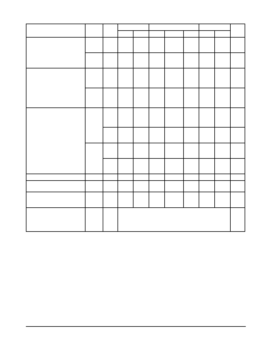
BLOCK DIAGRAM
This device contains protection circuitry to
guard against damage due to high static
voltages or electric fields. However, pre-
cautions must be taken to avoid applications of
any voltage higher than maximum rated volt-
ages to this highimpedance circuit. For proper
operation, Vin and Vout should be constrained
to the range VSS
v
(Vin or Vout)
v
VDD.
Unused inputs must always be tied to an
appropriate logic voltage level (e.g., either VSS
or VDD). Unused outputs must be left open.
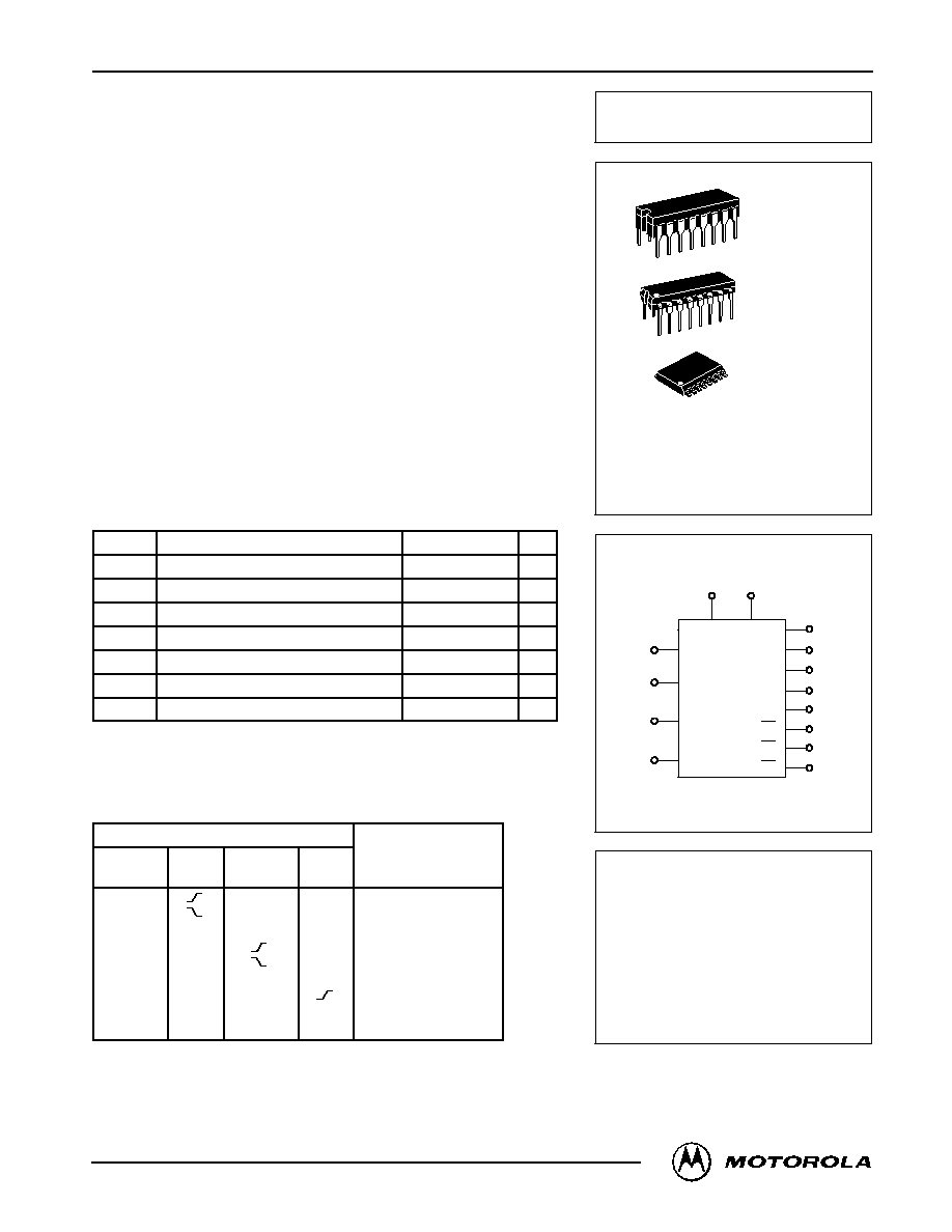
L SUFFIX
CERAMIC
CASE 620
ORDERING INFORMATION
MC14XXXBCP
Plastic
MC14XXXBCL
Ceramic
MC14XXXBDW
SOIC
TA = 55
°
to 125
°
C for all packages.
P SUFFIX
PLASTIC
CASE 648
DW SUFFIX
SOIC
CASE 751G
12
10
11
13
9
7
6
5
14
2
1
15
VDD = PIN 16
VSS = PIN 8
4
3
CLOCK
LE
DIS
MR
Q0
Q1
Q2
Q3
O.F.
DS1
DS2
DS3
CIA
CIB
MOTOROLA CMOS LOGIC DATA
MC14553B
2
ÎÎÎÎÎÎÎÎÎÎÎÎÎÎÎÎÎÎÎÎÎÎÎÎÎÎÎÎÎÎÎÎÎÎ
ÎÎÎÎÎÎÎÎÎÎÎÎÎÎÎÎÎÎÎÎÎÎÎÎÎÎÎÎÎÎÎÎÎÎ
ÎÎÎÎÎÎÎÎÎÎÎÎÎÎÎÎÎÎÎÎÎÎÎÎÎÎÎÎÎÎÎÎÎÎ
ÎÎÎÎÎÎÎÎÎÎÎÎÎÎÎÎÎÎÎÎÎÎÎÎÎÎÎÎÎÎÎÎÎÎ
ELECTRICAL CHARACTERISTICS
(Voltages Referenced to VSS)
Characteristic
Symbol
VDD
Vdc
55
_
C
25
_
C
125
_
C
Unit
Characteristic
Symbol
VDD
Vdc
Min
Max
Min
Typ #
Max
Min
Max
Unit
Output Voltage
"0" Level
Vin = VDD or 0
VOL
5.0
10
15
--
--
--
0.05
0.05
0.05
--
--
--
0
0
0
0.05
0.05
0.05
--
--
--
0.05
0.05
0.05
Vdc
"1" Level
Vin = 0 or VDD
VOH
5.0
10
15
4.95
9.95
14.95
--
--
--
4.95
9.95
14.95
5.0
10
15
--
--
--
4.95
9.95
14.95
--
--
--
Vdc
Input Voltage
"0" Level
(VO = 4.5 or 0.5 Vdc)
(VO = 9.0 or 1.0 Vdc)
(VO = 13.5 or 1.5 Vdc)
VIL
5.0
10
15
--
--
--
1.5
3.0
4.0
--
--
--
2.25
4.50
6.75
1.5
3.0
4.0
--
--
--
1.5
3.0
4.0
Vdc
"1" Level
(VO = 0.5 or 4.5 Vdc)
(VO = 1.0 or 9.0 Vdc)
(VO = 1.5 or 13.5 Vdc)
VIH
5.0
10
15
3.5
7.0
11
--
--
--
3.5
7.0
11
2.75
5.50
8.25
--
--
--
3.5
7.0
11
--
--
--
Vdc
Output Drive Current
(VOH = 4.6 Vdc)
Source --
(VOH = 9.5 Vdc)
Pin 3
(VOH = 13.5 Vdc)
IOH
5.0
10
15
0.25
0.62
1.8
--
--
--
0.2
0.5
1.5
0.36
0.9
3.5
--
--
--
0.14
0.35
1.1
--
--
--
mAdc
(VOH = 4.6 Vdc)
Source --
(VOH = 9.5 Vdc)
Other
(VOH = 13.5 Vdc)
Outputs
5.0
10
15
0.64
1.6
4.2
--
--
--
0.51
1.3
3.4
0.88
2.25
8.8
--
--
--
0.36
0.9
2.4
--
--
--
mAdc
(VOL = 0.4 Vdc)
Sink --
(VOL = 0.5 Vdc)
Pin 3
(VOL = 1.5 Vdc)
IOL
5.0
10
15
0.5
1.1
1.8
--
--
--
0.4
0.9
1.5
0.88
2.25
8.8
--
--
--
0.28
0.65
1.20
--
--
--
mAdc
(VOL = 0.4 Vdc) Sink -- Other
(VOL = 0.5 Vdc)
Outputs
(VOL = 1.5 Vdc)
5.0
10
15
3.0
6.0
18
--
--
--
2.5
5.0
15
4.0
8.0
20
--
--
--
1.6
3.5
10
--
--
--
mAdc
Input Current
Iin
15
--
±
0.1
--
±
0.00001
±
0.1
--
±
1.0
µ
Adc
Input Capacitance
(Vin = 0)
Cin
--
--
--
--
5.0
7.5
--
--
pF
Quiescent Current
(Per Package)
MR = VDD
IDD
5.0
10
15
--
--
--
5.0
10
20
--
--
--
0.010
0.020
0.030
5.0
10
20
--
--
--
150
300
600
µ
Adc
Total Supply Current**
(Dynamic plus Quiescent,
Per Package)
(CL = 50 pF on all outputs, all
buffers switching)
IT
5.0
10
15
IT = (0.35
µ
A/kHz) f + IDD
IT = (0.85
µ
A/kHz) f + IDD
IT = (1.50
µ
A/kHz) f + IDD
µ
Adc
#Data labelled "Typ" is not to be used for design purposes but is intended as an indication of the IC's potential performance.
** The formulas given are for the typical characteristics only at 25
_
C.
To calculate total supply current at loads other than 50 pF:
IT(CL) = IT(50 pF) + (CL 50) Vfk
where: IT is in
µ
A (per package), CL in pF, V = (VDD VSS) in volts, f in kHz is input frequency, and k = 0.004.
MOTOROLA CMOS LOGIC DATA
3
MC14553B
ÎÎÎÎÎÎÎÎÎÎÎÎÎÎÎÎÎÎÎÎÎÎÎÎÎÎÎÎÎÎÎÎÎÎ
ÎÎÎÎÎÎÎÎÎÎÎÎÎÎÎÎÎÎÎÎÎÎÎÎÎÎÎÎÎÎÎÎÎÎ
ÎÎÎÎÎÎÎÎÎÎÎÎÎÎÎÎÎÎÎÎÎÎÎÎÎÎÎÎÎÎÎÎÎÎ
ÎÎÎÎÎÎÎÎÎÎÎÎÎÎÎÎÎÎÎÎÎÎÎÎÎÎÎÎÎÎÎÎÎÎ
SWITCHING CHARACTERISTICS
(CL = 50 pF, TA = 25
_
C)
Characteristic
Figure
Symbol
VDD
Min
Typ #
Max
Unit
Output Rise and Fall Time
tTLH, tTHL = (1.5 ns/pF) CL + 25 ns
tTLH, tTHL = (0.75 ns/pF) CL + 12.5 ns
tTLH, tTHL = (0.55 ns/pF) CL + 9.5 ns
2a
tTLH,
tTHL
5.0
10
15
--
--
--
100
50
40
200
100
80
ns
Clock to BCD Out
2a
tPLH,
tPHL
5.0
10
15
--
--
--
900
500
200
1800
1000
400
ns
Clock to Overflow
2a
tPHL
5.0
10
15
--
--
--
600
400
200
1200
800
400
ns
Reset to BCD Out
2b
tPHL
5.0
10
15
--
--
--
900
500
300
1800
1000
600
ns
Clock to Latch Enable Setup Time
Master Reset to Latch Enable Setup Time
2b
tsu
5.0
10
15
600
400
200
300
200
100
--
--
--
ns
Removal Time
Latch Enable to Clock
2b
trem
5.0
10
15
80
10
0
200
70
50
--
--
--
ns
Clock Pulse Width
2a
tWH(cl)
5.0
10
15
550
200
150
275
100
75
--
--
--
ns
Reset Pulse Width
2b
tWH(R)
5.0
10
15
1200
600
450
600
300
225
--
--
--
ns
Reset Removal Time
--
trem
5.0
10
15
80
0
20
180
50
30
--
--
--
ns
Input Clock Frequency
2a
fcl
5.0
10
15
--
--
--
1.5
5.0
7.0
0.9
2.5
3.5
MHz
Input Clock Rise Time
2b
tTLH
5.0
10
15
No
Limit
ns
Disable, MR, Latch Enable
Rise and Fall Times
--
tTLH,
tTHL
5.0
10
15
--
--
--
--
--
--
15
5.0
4.0
µ
s
Scan Oscillator Frequency
(C1 measured in
µ
F)
1
fosc
5.0
10
15
--
--
--
1.5/C1
4.2/C1
7.0/C1
--
--
--
Hz
* The formulas given are for the typical characteristics only at 25
_
C.
#Data labelled "Typ" is not to be used for design purposes but is intended as an indication of the IC's potential performance.
MOTOROLA CMOS LOGIC DATA
MC14553B
4
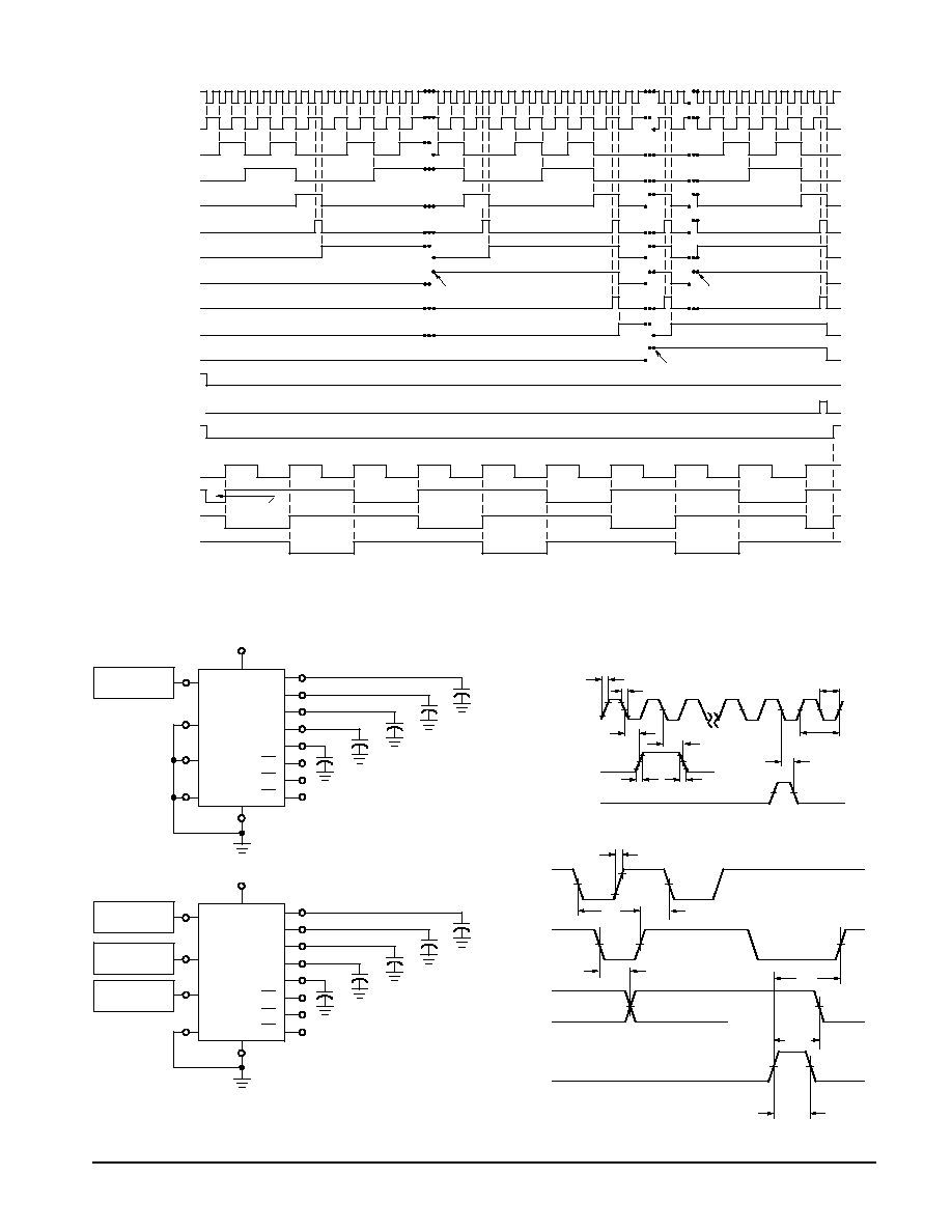
Figure 1. 3Digit Counter Timing Diagram (Reference Figure 3)
1000
999
998
997
996
995
994
993
992
991
990
901
900
899
101
100
99
98
97
96
95
94
93
92
91
90
89
88
87
86
17
16
15
14
13
12
1
1
10
9
8
7
6
5
4
3
2
1
UNITS CLOCK
UNITS Q0
UNITS Q1
UNITS Q2
UNITS Q3
TENS CLOCK
TENS Q0
TENS Q3
HUNDREDS
CLOCK
HUNDREDS Q0
HUNDREDS Q3
DISABLE
OVERFLOW
MASTER
RESET
SCAN
OSCILLATOR
DIGIT SELECT 1
DIGIT SELECT 2
DIGIT SELECT 3
UP AT 80
UP AT 980
UP AT 800
(DISABLES CLOCK WHEN HIGH)
UNITS
TENS
HUNDREDS
PULSE
GENERATOR
(a)
16
VDD
Q3
Q2
Q1
Q0
O.F.
DS1
DS2
DS3
8
VSS
C
LE
DIS
MR
CL
CL
CL
CL
CL
GENERATOR
1
(b)
VDD
Q3
Q2
Q1
Q0
O.F.
DS1
DS2
DS3
VSS
C
LE
MR
DIS
CL
CL
CL
CL
CL
GENERATOR
2
GENERATOR
3
20 ns
20 ns
90%
10%
tPLH
tPHL
50%
50%
tTHL
tTLH
10%
90%
50%
1/fcl
tWL(cl)
999
1000
tTLH
50%
OVERFLOW
BCD OUT
CLOCK
90%
10%
trem
tPHL, tPLH
50%
50%
50%
tWH(R)
tsu
tPHL
MASTER RESET
BCD OUT
LATCH
ENABLE
CLOCK
Figure 2. Switching Time Test Circuits and Waveforms
tsu
tPHL
MOTOROLA CMOS LOGIC DATA
5
MC14553B
OPERATING CHARACTERISTICS
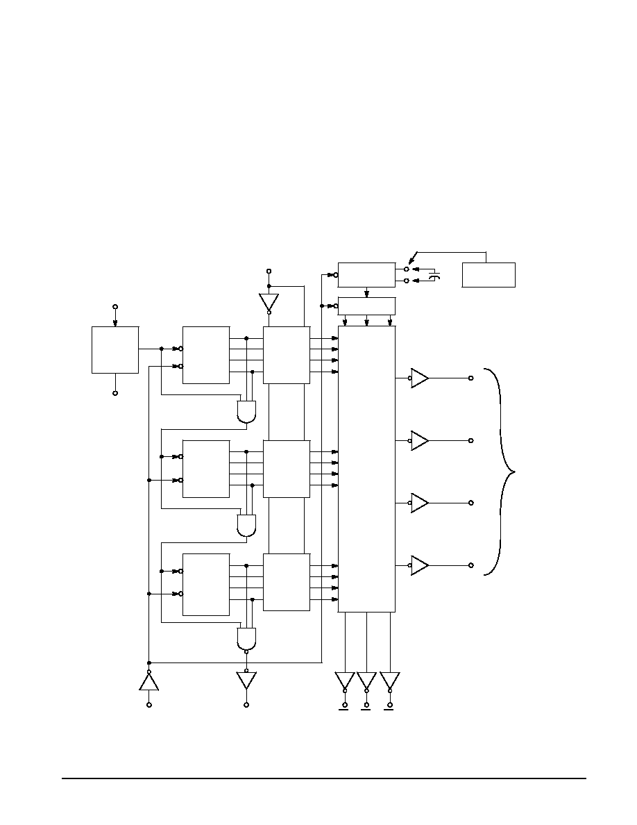
The MC14553B threedigit counter, shown in Figure 3,
consists of three negative edgetriggered BCD counters
which are cascaded in a synchronous fashion. A quad latch
at the output of each of the three BCD counters permits stor-
age of any given count. The three sets of BCD outputs
(active high), after going through the latches, are time divi-
sion multiplexed, providing one BCD number or digit at a
time. Digit select outputs (active low) are provided for display
control. All outputs are TTL compatible.
An onchip oscillator provides the low frequency scanning
clock which drives the multiplexer output selector. The fre-
quency of the oscillator can be controlled externally by a
capacitor between pins 3 and 4, or it can be overridden and
driven with an external clock at pin 4. Multiple devices can be
cascaded using the overflow output, which provides one
pulse for every 1000 counts.
The Master Reset input, when taken high, initializes the
three BCD counters and the multiplexer scanning circuit.
While Master Reset is high the digit scanner is set to digit
one; but all three digit select outputs are disabled to prolong
display life, and the scan oscillator is inhibited. The Disable
input, when high, prevents the input clock from reaching the
counters, while still retaining the last count. A pulse shaping
circuit at the clock input permits the counters to continue op-
erating on input pulses with very slow rise times. Information
present in the counters when the latch input goes high, will
be stored in the latches and will be retained while the latch
input is high, independent of other inputs. Information can be
recovered from the latches after the counters have been re-
set if Latch Enable remains high during the entire reset cycle.
Figure 3. Expanded Block Diagram
PULSE
SHAPER
CLOCK
12
11
DISABLE
(ACTIVE
HIGH)
C
R
Q0
Q1
Q2
Q3
÷
10
UNITS
C
R
Q0
Q1
Q2
Q3
÷
10
TENS
C
R
Q0
Q1
Q2
Q3
÷
10
HUNDREDS
10
LATCH ENABLE
QUAD
LATCH
QUAD
LATCH
QUAD
LATCH
R
R
SCAN
OSCILLATOR
SCANNER
PULSE
GENERATOR
C1
4
3
C1A
C1B
MULTIPLEXER
9
7
6
5
Q0
Q1
Q2
Q3
BCD
OUTPUTS
(ACTIVE
HIGH)
13
14
2
1
15
MR
(ACTIVE HIGH)
OVERFLOW
DS1
DS2
DS3
(LSD) DIGIT SELECT (MSD)
(ACTIVE LOW)
MOTOROLA CMOS LOGIC DATA
MC14553B
6
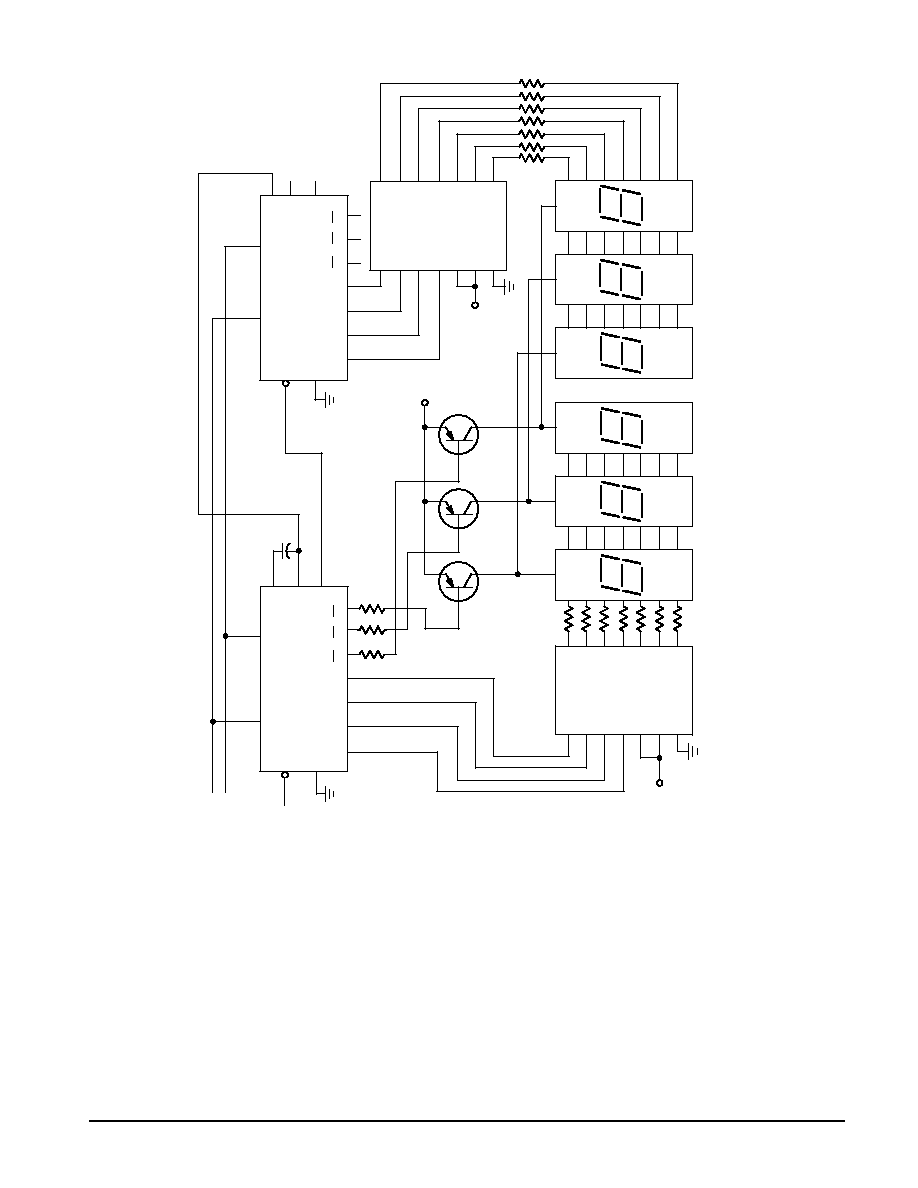
Figure 4. SixDigit Display
V
DD
STROBE
RESET
CLOCK
INPUT
10
13
5
6
7
9
15
1
2
14
3
4
12
1
1
CLK
DIS
Q3
Q2
Q1
Q0
DS3
DS2
DS1
C1
A
C1
B
O.F
.
µ
0.001
F
5
3
2
4
6
1
7
A
B
C
D
Ph
LD
BI
a
b
c
d
e
f
g
9
10
1
1
12
13
15
14
MC14543B
LSD
V
DD
DISPLA
YS
ARE LOW CURRENT
LEDs
(I
peak
< 10 mA
PER SEGMENT)
MSD
V
DD
5
3
2
4
6
1
7
A
B
C
D
Ph
LD
BI
a
b
c
d
e
f
g
9
10
1
1
12
13
15
14
MC14543B
10
13
5
6
7
9
15
1
2
14
3
4
12
1
1
CLK
DIS
Q3
Q2
Q1
Q0
DS3
DS2
DS1
C1
A
C1
B
O.F
.
MC14553B
MC14553B
LE
MR
LE
MR
MOTOROLA CMOS LOGIC DATA
7
MC14553B
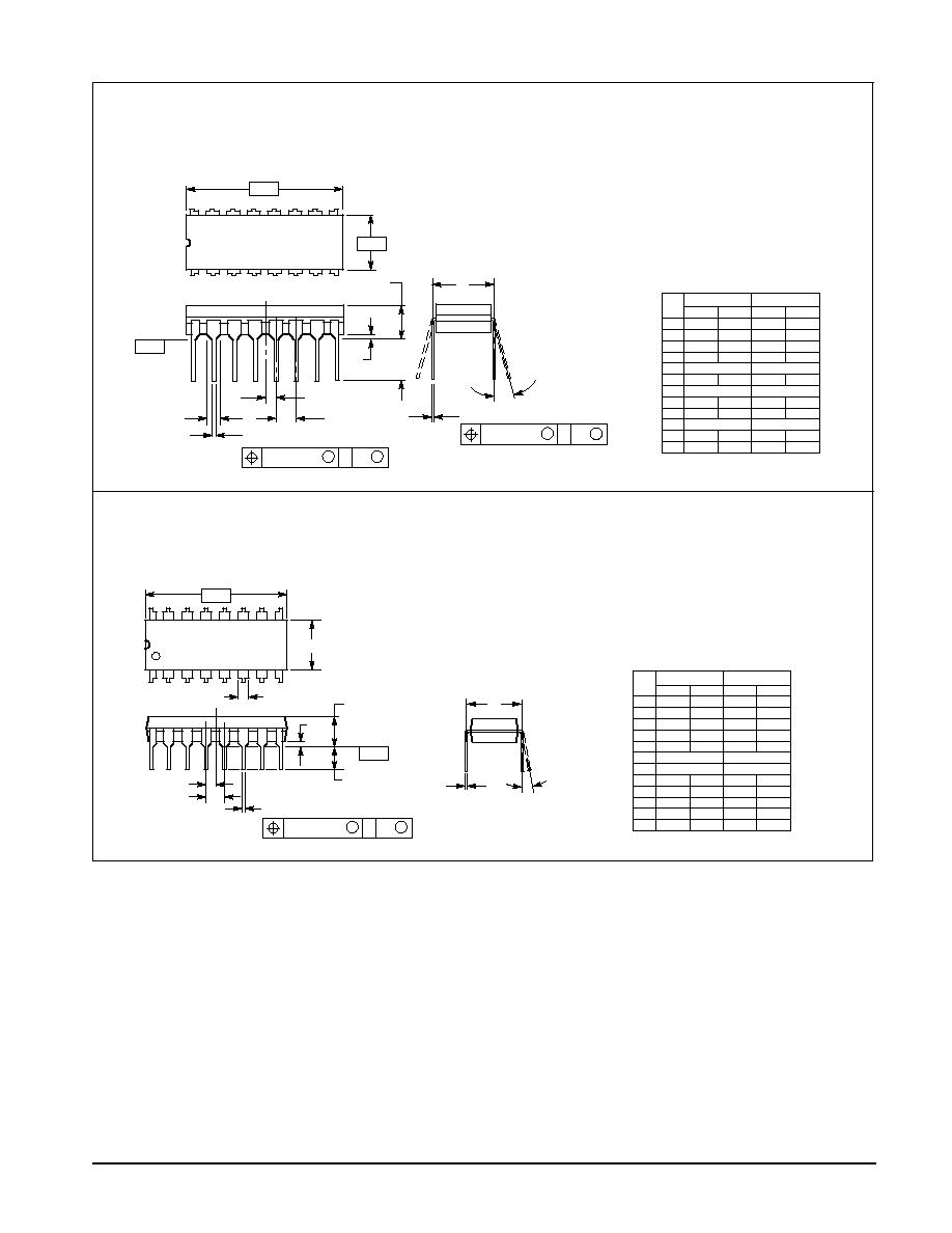
OUTLINE DIMENSIONS
P SUFFIX
PLASTIC DIP PACKAGE
CASE 64808
ISSUE R
NOTES:
1. DIMENSIONING AND TOLERANCING PER ANSI
Y14.5M, 1982.
2. CONTROLLING DIMENSION: INCH.
3. DIMENSION L TO CENTER OF LEADS WHEN
FORMED PARALLEL.
4. DIMENSION B DOES NOT INCLUDE MOLD FLASH.
5. ROUNDED CORNERS OPTIONAL.
A
B
F
C
S
H
G
D
J
L
M
16 PL
SEATING
1
8
9
16
K
PLANE
T
M
A
M
0.25 (0.010)
T
DIM
MIN
MAX
MIN
MAX
MILLIMETERS
INCHES
A
0.740
0.770
18.80
19.55
B
0.250
0.270
6.35
6.85
C
0.145
0.175
3.69
4.44
D
0.015
0.021
0.39
0.53
F
0.040
0.70
1.02
1.77
G
0.100 BSC
2.54 BSC
H
0.050 BSC
1.27 BSC
J
0.008
0.015
0.21
0.38
K
0.110
0.130
2.80
3.30
L
0.295
0.305
7.50
7.74
M
0
10
0
10
S
0.020
0.040
0.51
1.01
_
_
_
_
L SUFFIX
CERAMIC DIP PACKAGE
CASE 62010
ISSUE V
NOTES:
1. DIMENSIONING AND TOLERANCING PER
ANSI Y14.5M, 1982.
2. CONTROLLING DIMENSION: INCH.
3. DIMENSION L TO CENTER OF LEAD WHEN
FORMED PARALLEL.
4. DIMENSION F MAY NARROW TO 0.76 (0.030)
WHERE THE LEAD ENTERS THE CERAMIC
BODY.
A
B
T
F
E
G
N
K
C
SEATING
PLANE
16 PL
D
S
A
M
0.25 (0.010)
T
16 PL
J
S
B
M
0.25 (0.010)
T
M
L
DIM
MIN
MAX
MIN
MAX
MILLIMETERS
INCHES
A
0.750
0.785
19.05
19.93
B
0.240
0.295
6.10
7.49
C
0.200
5.08
D
0.015
0.020
0.39
0.50
E
0.050 BSC
1.27 BSC
F
0.055
0.065
1.40
1.65
G
0.100 BSC
2.54 BSC
H
0.008
0.015
0.21
0.38
K
0.125
0.170
3.18
4.31
L
0.300 BSC
7.62 BSC
M
0
15
0
15
N
0.020
0.040
0.51
1.01
_
_
_
_
16
9
1
8
MOTOROLA CMOS LOGIC DATA
MC14553B
8
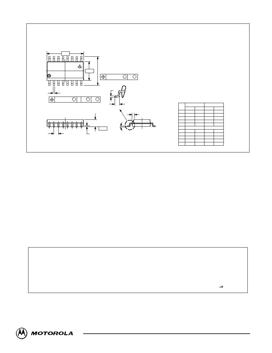
OUTLINE DIMENSIONS
DW SUFFIX
PLASTIC SOIC PACKAGE
CASE 751G02
ISSUE A
DIM
MIN
MAX
MIN
MAX
INCHES
MILLIMETERS
A
10.15
10.45
0.400
0.411
B
7.40
7.60
0.292
0.299
C
2.35
2.65
0.093
0.104
D
0.35
0.49
0.014
0.019
F
0.50
0.90
0.020
0.035
G
1.27 BSC
0.050 BSC
J
0.25
0.32
0.010
0.012
K
0.10
0.25
0.004
0.009
M
0
7
0
7
P
10.05
10.55
0.395
0.415
R
0.25
0.75
0.010
0.029
M
B
M
0.010 (0.25)
NOTES:
1. DIMENSIONING AND TOLERANCING PER ANSI
Y14.5M, 1982.
2. CONTROLLING DIMENSION: MILLIMETER.
3. DIMENSIONS A AND B DO NOT INCLUDE MOLD
PROTRUSION.
4. MAXIMUM MOLD PROTRUSION 0.15 (0.006) PER
SIDE.
5. DIMENSION D DOES NOT INCLUDE DAMBAR
PROTRUSION. ALLOWABLE DAMBAR
PROTRUSION SHALL BE 0.13 (0.005) TOTAL IN
EXCESS OF D DIMENSION AT MAXIMUM
MATERIAL CONDITION.
A
B
P
8X
G
14X
D
16X
SEATING
PLANE
T
S
A
M
0.010 (0.25)
B
S
T
16
9
8
1
F
J
R
X 45
_
_
_
_
_
M
C
K
How to reach us:
USA/EUROPE/Locations Not Listed: Motorola Literature Distribution;
JAPAN: Nippon Motorola Ltd.; TatsumiSPDJLDC, 6F SeibuButsuryuCenter,
P.O. Box 20912; Phoenix, Arizona 85036. 18004412447 or 6023035454
3142 Tatsumi KotoKu, Tokyo 135, Japan. 038135218315
MFAX: RMFAX0@email.sps.mot.com TOUCHTONE 6022446609
ASIA/PACIFIC: Motorola Semiconductors H.K. Ltd.; 8B Tai Ping Industrial Park,
INTERNET: http://DesignNET.com
51 Ting Kok Road, Tai Po, N.T., Hong Kong. 85226629298
Motorola reserves the right to make changes without further notice to any products herein. Motorola makes no warranty, representation or guarantee regarding
the suitability of its products for any particular purpose, nor does Motorola assume any liability arising out of the application or use of any product or circuit,
and specifically disclaims any and all liability, including without limitation consequential or incidental damages. "Typical" parameters which may be provided
in Motorola data sheets and/or specifications can and do vary in different applications and actual performance may vary over time. All operating parameters,
including "Typicals" must be validated for each customer application by customer's technical experts. Motorola does not convey any license under its patent
rights nor the rights of others. Motorola products are not designed, intended, or authorized for use as components in systems intended for surgical implant
into the body, or other applications intended to support or sustain life, or for any other application in which the failure of the Motorola product could create a
situation where personal injury or death may occur. Should Buyer purchase or use Motorola products for any such unintended or unauthorized application,
Buyer shall indemnify and hold Motorola and its officers, employees, subsidiaries, affiliates, and distributors harmless against all claims, costs, damages, and
expenses, and reasonable attorney fees arising out of, directly or indirectly, any claim of personal injury or death associated with such unintended or
unauthorized use, even if such claim alleges that Motorola was negligent regarding the design or manufacture of the part. Motorola and
are registered
trademarks of Motorola, Inc. Motorola, Inc. is an Equal Opportunity/Affirmative Action Employer.
MC14553B/D
*MC14553B/D*