MOTOROLA
SEMICONDUCTOR TECHNICAL DATA
4¡1
REV 2
®
Motorola, Inc. 1996
4/95
Low Voltage Quad
Differential Receiver
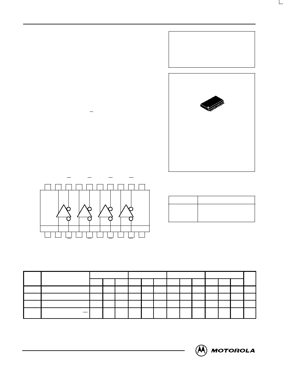
The MC100LVEL17 is a low-voltage, quad differential receiver. The
device is functionally equivalent to the E116 device with the capability of
operation from either a ¡3.3V or +3.3V supply voltage. The MC100EL17
is pin and functionally equivalent to the MC100LVEL17, but is specified
for operation at the standard 100E ECL voltage supply.
The LVEL17 provides a VBB output for either single-ended use or as a
DC bias for AC coupling to the device. The VBB pin should be used only
as a bias for the LVEL17 as its current sink/source capability is limited.
Whenever used, the VBB pin should be bypassed to ground via a 0.01
Á
f
capacitor.
Under open input conditions, the D input will be biased at VCC/2 and
the D input will be pulled down to VEE. This operation will force the Q
output LOW and ensure stability.
À
325ps Propagation Delay
À
High Bandwidth Output Transitions
À
>2000V ESD Protection
À
Operates from ¡3.3/¡4.5V (or +3.3/+5.0V) Supply
D1
Logic Diagram and Pinout: 20-Lead SOIC (Top View)
D1
D2
D3
17
18
16
15
14
13
12
4
3
5
6
7
8
9
Q0
11
10
Q1
Q1
Q2
Q2
Q3
Q3
VEE
D0
19
20
2
1
VCC
Q0
D0
D2
VCC
D3
VBB
MC100LVEL17
DC CHARACTERISTICS (VEE = ¡3.0V to ¡3.8V; VCC = GND) Note 1
¡40
░
C
0
░
C
25
░
C
85
░
C
Symbol
Characteristic
Min
Typ
Max
Min
Typ
Max
Min
Typ
Max
Min
Typ
Max
Unit
IEE
Power Supply Current
26
31
26
31
26
31
27
33
mA
VBB
Output Reference Voltage
¡1.38
¡1.26
¡1.38
¡1.26
¡1.38
¡1.26
¡1.38
¡1.26
V
IIH
Input HIGH Current
150
150
150
150
Á
A
IINL
Input LOW Current
Dn
Dn
0.5
¡300
0.5
¡300
0.5
¡300
0.5
¡300
Á
A
1. All other DC characteristics are the same as Standard 100K ECL.
MC100LVEL17
MC100EL17
DW SUFFIX
PLASTIC SOIC PACKAGE
CASE 751D-04
1
20
PIN NAMES
Function
Data Inputs
Data Outputs
Reference Voltage Output
Pins
Dn
Qn
VBB
MC100LVEL17 MC100EL17
MOTOROLA
ECLinPS and ECLinPS Lite
DL140 -- Rev 3
4¡2
MC100LVEL17
AC CHARACTERISTICS (VEE = ¡3.0V to ¡3.8V; VCC = GND)
¡40
░
C
0
░
C
25
░
C
85
░
C
Symbol
Characteristic
Min
Typ
Max
Min
Typ
Max
Min
Typ
Max
Min
Typ
Max
Unit
tPLH
tPHL
Propagation Delay
Diff
D to Q
S.E.
330
280
530
580
340
290
540
590
350
300
550
600
360
310
560
610
ps
tSKEW
Skew Output¡to¡Output1
Part¡to¡Part (Diff)1
Duty Cycle (Diff)2
75
200
25
75
200
25
75
200
25
75
200
25
ps
VPP
Minimum Input Swing3
150
150
150
150
mV
VCMR
Common Mode Range4
VPP < 500mV
VPP
500mV
¡2.0
¡1.8
¡0.4
¡0.4
¡2.1
¡1.9
¡0.4
¡0.4
¡2.1
¡1.9
¡0.4
¡0.4
¡2.1
¡1.9
¡0.4
¡0.4
V
tr
tf
Output Rise/Fall Times Q
(20% ¡ 80%)
280
550
280
550
280
550
280
550
ps
1. Skews are valid across specified voltage range, part¡to¡part skew is for a given temperature.
2. Duty cycle skew is the difference between a TPLH and TPHL propagation delay through a device.
3. Minimum input swing for which AC parameters guaranteed. The device has a DC gain of
40.
4. The CMR range is referenced to the most positive side of the differential input signal. Normal operation is obtained if the HIGH level falls within
the specified range and the peak-to-peak voltage lies between VPPmin and 1V. The lower end of the CMR range varies 1:1 with VEE. The
numbers in the spec table assume a nominal VEE = ¡3.3V. Note for PECL operation, the VCMR(min) will be fixed at 3.3V ¡ |VCMR(min)|.
MC100EL17
DC CHARACTERISTICS (VEE = ¡4.2V to ¡5.5V; VCC = GND) Note 1
¡40
░
C
0
░
C
25
░
C
85
░
C
Symbol
Characteristic
Min
Typ
Max
Min
Typ
Max
Min
Typ
Max
Min
Typ
Max
Unit
IEE
Power Supply Current
26
31
26
31
26
31
27
33
mA
VBB
Output Reference Voltage
¡1.38
¡1.26
¡1.38
¡1.26
¡1.38
¡1.26
¡1.38
¡1.26
V
IIH
Input HIGH Current
150
150
150
150
Á
A
IINL
Input LOW Current
Dn
Dn
0.5
¡300
0.5
¡300
0.5
¡300
0.5
¡300
Á
A
1. All other DC characteristics are the same as Standard 100K ECL.
MC100EL17
AC CHARACTERISTICS (VEE = ¡4.20V to ¡5.5V; VCC = GND)
¡40
░
C
0
░
C
25
░
C
85
░
C
Symbol
Characteristic
Min
Typ
Max
Min
Typ
Max
Min
Typ
Max
Min
Typ
Max
Unit
tPLH
tPHL
Propagation Delay
Diff
D to Q
S.E.
330
280
530
580
340
290
540
590
350
300
550
600
360
310
560
610
ps
tSKEW
Skew Output¡to¡Output1
Part¡to¡Part (Diff)1
Duty Cycle (Diff)2
75
200
25
75
200
25
75
200
25
75
200
25
ps
VPP
Minimum Input Swing3
150
150
150
150
mV
VCMR
Common Mode Range4
VPP < 500mV
VPP
500mV
¡3.2
¡3.0
¡0.4
¡0.4
¡3.3
¡3.1
¡0.4
¡0.4
¡3.3
¡3.1
¡0.4
¡0.4
¡3.3
¡3.1
¡0.4
¡0.4
V
tr
tf
Output Rise/Fall Times Q
(20% ¡ 80%)
280
550
280
550
280
550
280
550
ps
1. Skews are valid across specified voltage range, part¡to¡part skew is for a given temperature.
2. Duty cycle skew is the difference between a TPLH and TPHL propagation delay through a device.
3. Minimum input swing for which AC parameters guaranteed. The device has a DC gain of
40.
4. The CMR range is referenced to the most positive side of the differential input signal. Normal operation is obtained if the HIGH level falls within
the specified range and the peak-to-peak voltage lies between VPPmin and 1V. The lower end of the CMR range varies 1:1 with VEE. The
numbers in the spec table assume a nominal VEE = ¡4.5V. Note for PECL operation, the VCMR(min) will be fixed at 5.0V ¡ |VCMR(min)|.
MC100LVEL17 MC100EL17
4¡3
MOTOROLA
ECLinPS and ECLinPS Lite
DL140 -- Rev 3
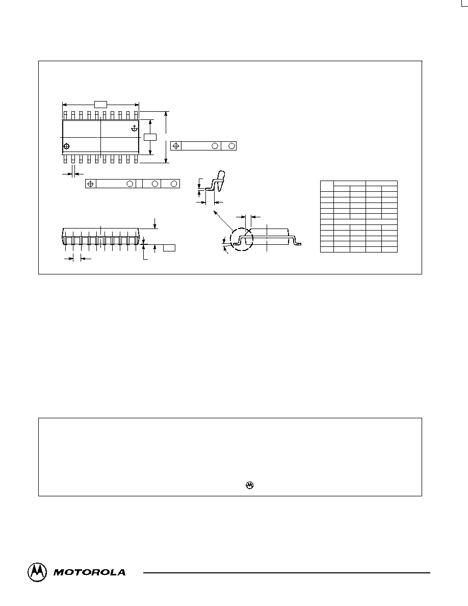
OUTLINE DIMENSIONS
DW SUFFIX
PLASTIC SOIC PACKAGE
CASE 751D¡04
ISSUE E
MIN
MIN
MAX
MAX
MILLIMETERS
INCHES
DIM
A
B
C
D
F
G
J
K
M
P
R
0.510
0.299
0.104
0.019
0.035
0.012
0.009
7
░
0.415
0.029
0.499
0.292
0.093
0.014
0.020
0.010
0.004
0
░
0.395
0.010
12.95
7.60
2.65
0.49
0.90
0.32
0.25
7
░
10.55
0.75
12.65
7.40
2.35
0.35
0.50
0.25
0.10
0
░
10.05
0.25
NOTES:
1. DIMENSIONING AND TOLERANCING PER
ANSI Y14.5M, 1982.
2. CONTROLLING DIMENSION: MILLIMETER.
3. DIMENSIONS A AND B DO NOT INCLUDE
MOLD PROTRUSION.
4. MAXIMUM MOLD PROTRUSION 0.150
(0.006) PER SIDE.
5. DIMENSION D DOES NOT INCLUDE
DAMBAR PROTRUSION. ALLOWABLE
DAMBAR PROTRUSION SHALL BE 0.13
(0.005) TOTAL IN EXCESS OF D DIMENSION
AT MAXIMUM MATERIAL CONDITION.
1.27 BSC
0.050 BSC
¡A
¡
¡B
¡
P
10 PL
1
10
11
20
¡T
¡
D
20 PL
K
C
SEATING
PLANE
R
X 45
░
M
0.010 (0.25)
B
M
M
0.010 (0.25)
T
A
B
M
S
S
G
18 PL
F
J
Motorola reserves the right to make changes without further notice to any products herein. Motorola makes no warranty, representation or guarantee regarding
the suitability of its products for any particular purpose, nor does Motorola assume any liability arising out of the application or use of any product or circuit, and
specifically disclaims any and all liability, including without limitation consequential or incidental damages. "Typical" parameters which may be provided in Motorola
data sheets and/or specifications can and do vary in different applications and actual performance may vary over time. All operating parameters, including "Typicals"
must be validated for each customer application by customer's technical experts. Motorola does not convey any license under its patent rights nor the rights of
others. Motorola products are not designed, intended, or authorized for use as components in systems intended for surgical implant into the body, or other
applications intended to support or sustain life, or for any other application in which the failure of the Motorola product could create a situation where personal injury
or death may occur. Should Buyer purchase or use Motorola products for any such unintended or unauthorized application, Buyer shall indemnify and hold Motorola
and its officers, employees, subsidiaries, affiliates, and distributors harmless against all claims, costs, damages, and expenses, and reasonable attorney fees
arising out of, directly or indirectly, any claim of personal injury or death associated with such unintended or unauthorized use, even if such claim alleges that
Motorola was negligent regarding the design or manufacture of the part. Motorola and are registered trademarks of Motorola, Inc. Motorola, Inc. is an Equal
Opportunity/Affirmative Action Employer.
How to reach us:
USA/EUROPE/Locations Not Listed: Motorola Literature Distribution;
JAPAN: Nippon Motorola Ltd.; Tatsumi¡SPD¡JLDC, 6F Seibu¡Butsuryu¡Center,
P.O. Box 20912; Phoenix, Arizona 85036. 1¡800¡441¡2447 or 602¡303¡5454
3¡14¡2 Tatsumi Koto¡Ku, Tokyo 135, Japan. 03¡81¡3521¡8315
MFAX: RMFAX0@email.sps.mot.com ¡ TOUCHTONE 602¡244¡6609
ASIA/PACIFIC: Motorola Semiconductors H.K. Ltd.; 8B Tai Ping Industrial Park,
INTERNET: http://Design¡NET.com
51 Ting Kok Road, Tai Po, N.T., Hong Kong. 852¡26629298
MC100LVEL17/D
*MC100LVEL17/D*