MOTOROLA
SEMICONDUCTOR TECHNICAL DATA
2ş1
REV 3
ę
Motorola, Inc. 1996
5/95
Quint Differential Line
Receiver
The MC10E/100E116 is a quint differential line receiver with
emitter-follower outputs. An internally generated reference supply (VBB)
is available for single-ended reception.
Ě
500ps Max. Propagation Delay
Ě
VBB Supply Output
Ě
Dedicated VCCO Pin for Each Receiver
Ě
Extended 100E VEE Range of ş 4.2V to ş 5.46V
Ě
75k
Input Pulldown Resistors
Active current sources plus a deep collector feature of the MOSAIC III
process provide the receivers with excellent common-mode noise
rejection. Each receiver has a dedicated VCCO supply lead, providing
optimum symmetry and stability.
The receiver design features clamp circuitry to cause a defined state if
both the inverting and non-inverting inputs are left open; in this case the Q
output goes LOW, while the Q output goes HIGH. This feature makes the
device ideal for twisted pair applications.
If both inverting and non-inverting inputs are at an equal potential of
> ş2.5V, the receiver does
not go to a defined state, but rather
current-shares in normal differential amplifier fashion, producing output
voltage levels midway between HIGH and LOW, or the device may even
oscillate.
The device VBB output is intended for use as a reference voltage for single-ended reception of ECL signals to that device only.
When using for this purpose, it is recommended that VBB is decoupled to VCC via a 0.01
Á
F capacitor. Please refer to the interface
section of the design guide for information on using the E116 in specialized applications.
The E116 features input pull-down resistors, as does the rest of the ECLinPS family. For applications which require
bandwidths greater than that of the E116, the E416 device may be of interest.
PIN NAMES
Pin
Function
D0, D0 ş D4, D4
Differential Input Pairs
Q0, Q0 ş Q4, Q4
Differential Output Pairs
VBB
Reference Voltage Output.
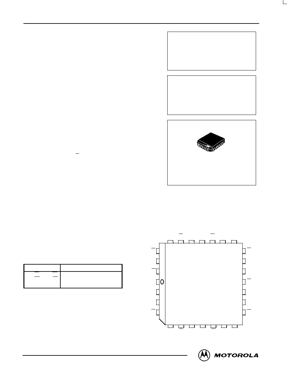
MC10E116
MC100E116
QUINT DIFFERENTIAL
LINE RECEIVER
FN SUFFIX
PLASTIC PACKAGE
CASE 776-02
VCCO
D1
D3
Q1
VCCO
Q0
Q0
D3
D2
D2
VEE
VBB
D0
D0
26
27
28
2
3
4
25
24
23
22
21
20
19
18
17
16
15
14
13
12
11
5
6
7
8
9
10
D4
D4 VCCO Q4
Q4
VCCO
Q3
Q3
VCC
Q2
Q2
VCCO
Q1
D1
1
Pinout: 28-Lead PLCC (Top View)
* All VCC and VCCO pins are tied together on the die.
MC10E116 MC100E116
MOTOROLA
ECLinPS and ECLinPS Lite
DL140 -- Rev 4
2ş2
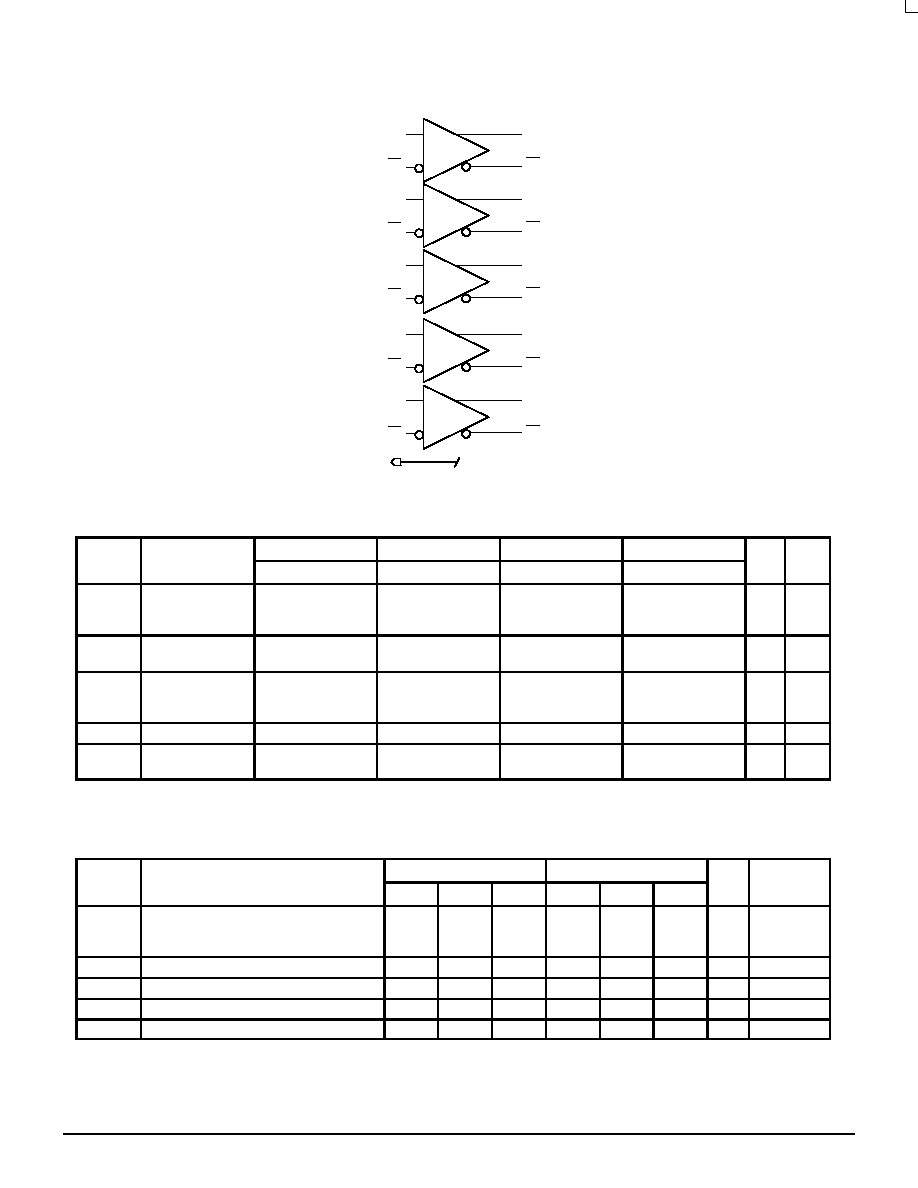
LOGIC DIAGRAM
D0
D0
D1
D1
D2
D2
D3
D3
D4
D4
VBB
Q0
Q0
Q1
Q1
Q2
Q2
Q3
Q3
Q4
Q4
DC CHARACTERISTICS (VEE = VEE(min) to VEE(max); VCC = VCCO = GND)
ş40
░
C
0
░
C
25
░
C
85
░
C
Symbol
Characteristic
Min
Typ
Max
Min
Typ
Max
Min
Typ
Max
Min
Typ
Max
Unit
Cond
VBB
Output Reference
Voltage
10E
100E
ş1.43
ş1.38
ş1.30
ş1.26
ş1.38
ş1.38
ş1.27
ş1.26
ş1.35
ş1.38
ş1.25
ş1.26
ş1.31
ş1.38
ş1.19
ş1.26
V
IIH
Input HIGH
Current
200
200
200
200
Á
A
IEE
Power Supply
Current
10E
100E
29
29
35
35
29
29
35
35
29
29
35
35
29
29
35
40
mA
VPP(DC)
Input Sensitivity
150
150
150
150
mV
1
VCMR
Commom Mode
Range
ş2.0
ş0.6
ş2.0
ş0.6
ş2.0
ş0.6
ş2.0
ş0.6
V
2
1. Differential input voltage required to obtain a full ECL swing on the outputs.
2. VCMR is defined as the range within which the VIH level may vary, with the device still meeting the propagation delay specification. The VIL level
must be such that the peak to peak
voltage is less than 1.0 V and greater than or equal to VPP(min).
AC CHARACTERISTICS (VEE = VEE (min) to VEE (max); VCC = VCCO = GND)
ş40
░
C
0
░
C to 85
░
C
Symbol
Characteristic
Min
Typ
Max
Min
Typ
Max
Unit
Condition
tPLH
tPHL
Propagation Delay to Output
D (Differential)
D (Single-Ended)
150
150
300
300
500
550
200
150
300
300
450
500
ps
tskew
Within-Device Skew
50
50
ps
1
tskew
Duty Cycle Skew
tPLH ş tPHL
▒
10
▒
10
ps
2
VPP(AC)
Minimum Input Swing
150
150
mV
3
tr/tf
Rise/Fall Time
250
375
625
275
375
575
ps
20ş80%
1. Within-device skew is defined as identical transitions on similar paths through a device.
2. Duty cycle skew is defined only for differential operation when the delays are measured from the cross point of the inputs to the cross point
of the outputs.
3. Minimum input swing for which AC parameters are guaranteed.
MC10E116 MC100E116
2ş3
MOTOROLA
ECLinPS and ECLinPS Lite
DL140 -- Rev 4
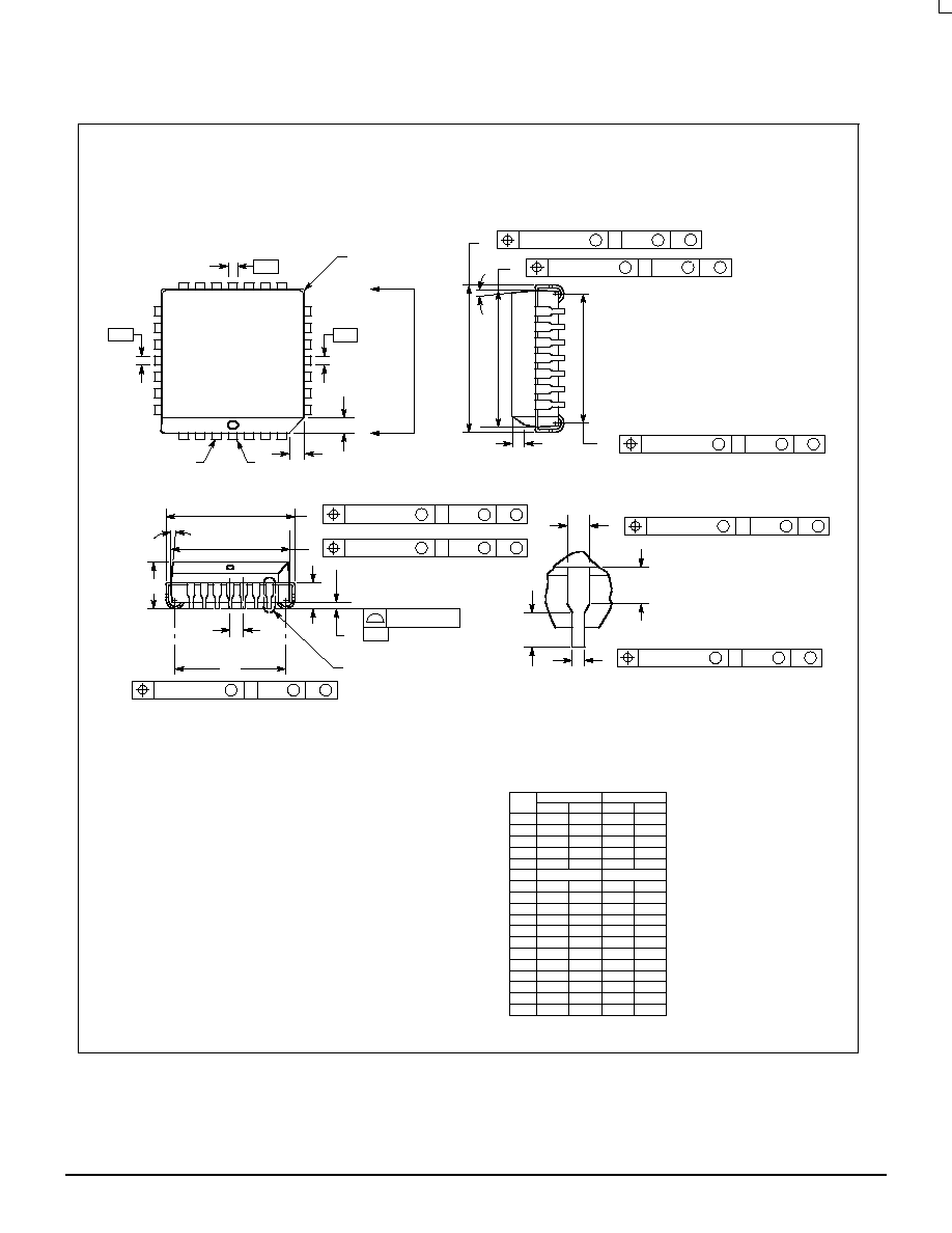
OUTLINE DIMENSIONS
FN SUFFIX
PLASTIC PLCC PACKAGE
CASE 776ş02
ISSUE D
0.007 (0.180)
T L şM
S
N
S
M
0.007 (0.180)
T L şM
S
N
S
M
0.007 (0.180)
T L şM
S
N
S
M
0.010 (0.250)
T L şM
S
N
S
S
0.007 (0.180)
T L şM
S
N
S
M
0.010 (0.250)
T L şM
S
N
S
S
0.007 (0.180)
T L şM
S
N
S
M
0.007 (0.180)
T L şM
S
N
S
M
0.004 (0.100)
SEATING
PLANE
-T-
12.32
12.32
4.20
2.29
0.33
0.66
0.51
0.64
11.43
11.43
1.07
1.07
1.07
--
2
░
10.42
1.02
12.57
12.57
4.57
2.79
0.48
0.81
--
--
11.58
11.58
1.21
1.21
1.42
0.50
10
░
10.92
--
1.27 BSC
A
B
C
E
F
G
H
J
K
R
U
V
W
X
Y
Z
G1
K1
MIN
MIN
MAX
MAX
INCHES
MILLIMETERS
DIM
NOTES:
1. DATUMS -L-, -M-, AND -N- DETERMINED
WHERE TOP OF LEAD SHOULDER EXITS
PLASTIC BODY AT MOLD PARTING LINE.
2. DIM G1, TRUE POSITION TO BE MEASURED
AT DATUM -T-, SEATING PLANE.
3. DIM R AND U DO NOT INCLUDE MOLD FLASH.
ALLOWABLE MOLD FLASH IS 0.010 (0.250)
PER SIDE.
4. DIMENSIONING AND TOLERANCING PER ANSI
Y14.5M, 1982.
5. CONTROLLING DIMENSION: INCH.
6. THE PACKAGE TOP MAY BE SMALLER THAN
THE PACKAGE BOTTOM BY UP TO 0.012
(0.300). DIMENSIONS R AND U ARE
DETERMINED AT THE OUTERMOST
EXTREMES OF THE PLASTIC BODY
EXCLUSIVE OF MOLD FLASH, TIE BAR
BURRS, GATE BURRS AND INTERLEAD
FLASH, BUT INCLUDING ANY MISMATCH
BETWEEN THE TOP AND BOTTOM OF THE
PLASTIC BODY.
7. DIMENSION H DOES NOT INCLUDE DAMBAR
PROTRUSION OR INTRUSION. THE DAMBAR
PROTRUSION(S) SHALL NOT CAUSE THE H
DIMENSION TO BE GREATER THAN 0.037
(0.940). THE DAMBAR INTRUSION(S) SHALL
NOT CAUSE THE H DIMENSION TO BE
SMALLER THAN 0.025 (0.635).
VIEW S
B
U
Z
G1
X
VIEW D-D
H
K
F
VIEW S
G
C
Z
A
R
E
J
0.485
0.485
0.165
0.090
0.013
0.026
0.020
0.025
0.450
0.450
0.042
0.042
0.042
--
2
░
0.410
0.040
0.495
0.495
0.180
0.110
0.019
0.032
--
--
0.456
0.456
0.048
0.048
0.056
0.020
10
░
0.430
--
0.050 BSC
-N-
Y BRK
D
D
W
-M-
-L-
28
1
V
G1
K1
MC10E116 MC100E116
MOTOROLA
ECLinPS and ECLinPS Lite
DL140 -- Rev 4
2ş4
Motorola reserves the right to make changes without further notice to any products herein. Motorola makes no warranty, representation or guarantee regarding
the suitability of its products for any particular purpose, nor does Motorola assume any liability arising out of the application or use of any product or circuit, and
specifically disclaims any and all liability, including without limitation consequential or incidental damages. "Typical" parameters which may be provided in Motorola
data sheets and/or specifications can and do vary in different applications and actual performance may vary over time. All operating parameters, including "Typicals"
must be validated for each customer application by customer's technical experts. Motorola does not convey any license under its patent rights nor the rights of
others. Motorola products are not designed, intended, or authorized for use as components in systems intended for surgical implant into the body, or other
applications intended to support or sustain life, or for any other application in which the failure of the Motorola product could create a situation where personal injury
or death may occur. Should Buyer purchase or use Motorola products for any such unintended or unauthorized application, Buyer shall indemnify and hold Motorola
and its officers, employees, subsidiaries, affiliates, and distributors harmless against all claims, costs, damages, and expenses, and reasonable attorney fees
arising out of, directly or indirectly, any claim of personal injury or death associated with such unintended or unauthorized use, even if such claim alleges that
Motorola was negligent regarding the design or manufacture of the part. Motorola and are registered trademarks of Motorola, Inc. Motorola, Inc. is an Equal
Opportunity/Affirmative Action Employer.
How to reach us:
USA/EUROPE/Locations Not Listed: Motorola Literature Distribution;
JAPAN: Nippon Motorola Ltd.; TatsumişSPDşJLDC, 6F SeibuşButsuryuşCenter,
P.O. Box 20912; Phoenix, Arizona 85036. 1ş800ş441ş2447 or 602ş303ş5454
3ş14ş2 Tatsumi KotoşKu, Tokyo 135, Japan. 03ş81ş3521ş8315
MFAX: RMFAX0@email.sps.mot.com ş TOUCHTONE 602ş244ş6609
ASIA/PACIFIC: Motorola Semiconductors H.K. Ltd.; 8B Tai Ping Industrial Park,
INTERNET: http://DesignşNET.com
51 Ting Kok Road, Tai Po, N.T., Hong Kong. 852ş26629298
MC10E116/D
*MC10E116/D*