
1
Motorola Thyristor Device Data
Triacs
Silicon Bidirectional Thyristors
. . . designed primarily for full-wave ac control applications, such as solid-state relays,
motor controls, heating controls and power supplies; or wherever full-wave silicon
gate controlled solid-state devices are needed. Triac type thyristors switch from a
blocking to a conducting state for either polarity of applied anode voltage with positive
or negative gate triggering.
·
Blocking Voltage to 800 Volts
·
All Diffused and Glass Passivated Junctions for Greater Parameter Uniformity
and Stability
·
Small, Rugged, Thermowatt Construction for Low Thermal Resistance, High Heat
Dissipation and Durability
·
Gate Triggering Guaranteed in Three Modes (MAC320 Series) or Four Modes
(MAC320A Series)
MAXIMUM RATINGS
(TC = 25
°
C unless otherwise noted.)
Rating
Symbol
Value
Unit
Peak Repetitive Off-State Voltage(1) (TJ = 40 to +125
°
C,
1/2 Sine Wave 50 to 60 Hz, Gate Open)
MAC320-4, MAC320A4
MAC320-6, MAC320A6
MAC320-8, MAC320A8
MAC320-10, MAC320A10
VDRM
200
400
600
800
Volts
Peak Gate Voltage
VGM
10
Volts
On-State Current RMS (TC = +75
°
C)
(Full Cycle, Sine Wave, 50 to 60 Hz)
IT(RMS)
20
Amp
Peak Surge Current (One Full Cycle, 60 Hz, TC = +75
°
C)
preceded and followed by rated current
ITSM
150
Amp
Peak Gate Power (TC = +75
°
C, Pulse Width = 2
µ
s)
PGM
20
Watts
Average Gate Power (TC = +75
°
C, t = 8.3 ms)
PG(AV)
0.5
Watt
Peak Gate Current
IGM
2
Amp
Operating Junction Temperature Range
TJ
40 to +125
°
C
Storage Temperature Range
Tstg
40 to +150
°
C
THERMAL CHARACTERISTICS
Characteristic
Symbol
Max
Unit
Thermal Resistance, Junction to Case
R
JC
1.8
°
C/W
1. VDRM for all types can be applied on a continuous basis. Blocking voltages shall not be tested with a constant current source such that the
voltage ratings of the devices are exceeded.
Order this document
by MAC320/D
MOTOROLA
SEMICONDUCTOR TECHNICAL DATA
©
Motorola, Inc. 1995
MAC320
Series
MAC320A
Series
CASE 221A-04
(TO-220AB)
STYLE 4
TRIACs
20 AMPERES RMS
200 thru 800 VOLTS
MT1
G
MT2

MAC320 Series MAC320A Series
2
Motorola Thyristor Device Data
ELECTRICAL CHARACTERISTICS
(TC = 25
°
C unless otherwise noted.)
Characteristic
Symbol
Min
Typ
Max
Unit
Peak Blocking Current
(VD Rated VDRM, Gate Open)
TJ = 25
°
C
TJ = +125
°
C
IDRM
--
--
--
--
10
2
µ
A
mA
Peak On-State Voltage (Either Direction)
(ITM = 28 A Peak; Pulse Width = 1 to 2 ms, Duty Cycle
p
2%)
VTM
--
1.4
1.7
Volts
Gate Trigger Current (Continuous dc)
(Main Terminal Voltage = 12 Vdc, RL = 100 Ohms)
MT2 (+), G(+); MT2 (+), G(); MT2 (), G()
MT2 (), G(+) "A" SUFFIX ONLY
IGT
--
--
--
--
50
75
mA
Gate Trigger Voltage (Continuous dc)
(Main Terminal Voltage = 12 Vdc, RL = 100 Ohms)
MT2 (+), G(+); MT2 (+), G(); MT2 (), G()
MT2 (), G(+) "A" SUFFIX ONLY
(Main Terminal Voltage = Rated VDRM, RL = 10 k
, TJ =+110
°
C)
MT2 (+), G(+); MT2 (), G(); MT2 (+), G();
MT2 (), G(+) "A" SUFFIX ONLY
VGT
--
--
0.2
0.2
0.9
1.4
--
--
2
2.5
--
--
Volts
Holding Current (Either Direction)
(Main Terminal Voltage = 12 Vdc, Gate Open,
Initiating Current = 200 mA)
IH
--
6
40
mA
Turn-On Time
(VD = Rated VDRM, ITM = 28 A,
IGT = 120 mA, Rise Time = 0.1
µ
s, Pulse Width = 2
µ
s)
tgt
--
1.5
--
µ
s
Critical Rate of Rise of Commutation Voltage
(VD = Rated VDRM, ITM = 28 A, Commutating
di/dt = 10 A/ms, Gate Unenergized, TC = +75
°
C)
dv/dt(C)
--
5
--
V/
µ
s
110
120
130
2.0
4.0
6.0
8.0
10
12
60
70
80
90
100
14
16
dc
0
FIGURE 1 -- RMS CURRENT DERATING
5.0
40
35
30
25
20
15
10
20
18
FIGURE 2 -- ON-STATE POWER DISSIPATION
IT(RMS), RMS ON-STATE CURRENT (AMP)
50
0
2.0
4.0
6.0
8.0
10
12
14
16
0
20
18
IT(RMS), RMS ON-STATE CURRENT (AMP)
= 30
°
180
°
= Conduction
Angle
= Conduction
Angle
P
D(A
V)
,
A
VERAGE POWER (W
A
TT)
T
C
, MAXIMUM
ALLOW
ABLE CASE
TEMPERA
TURE ( C)
°
180
°
dc
90
°
60
°
= 30
°
60
°
90
°
MAC320 Series MAC320A Series
3
Motorola Thyristor Device Data
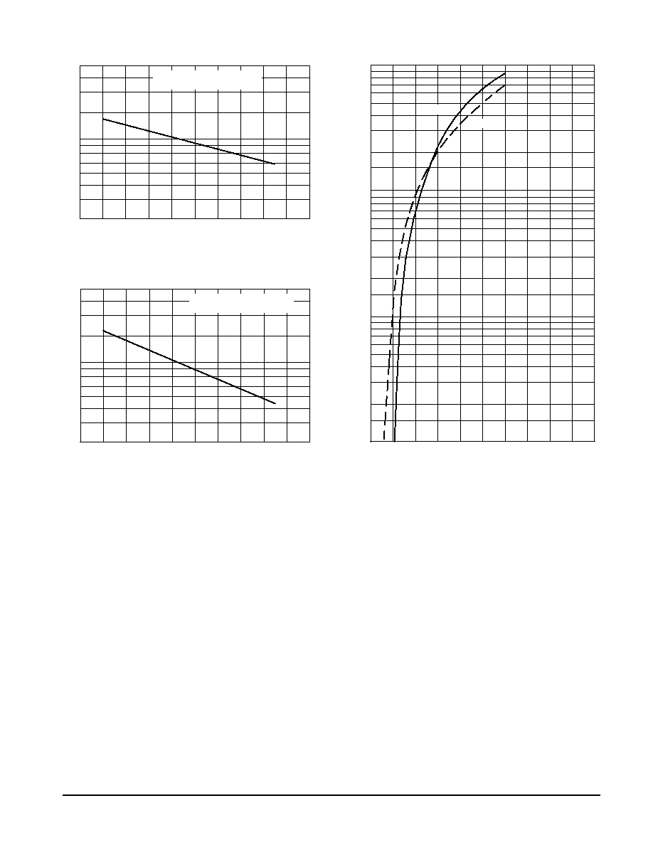
FIGURE 5 -- MAXIMUM ON-STATE CHARACTERISTICS
FIGURE 4 -- TYPICAL GATE TRIGGER CURRENT
FIGURE 3 -- TYPICAL GATE TRIGGER VOLTAGE
1
30
2
3
5
7
10
20
50
70
100
0.1
0.7
0.5
0.3
4
0.2
0.4
0.8
1.2
1.6
2
2.4
2.8
3.6
3.2
4.4
vTM, INSTANTANEOUS ON-STATE VOLTAGE (VOLTS)
i , INST
ANT
ANEOUS FOR
W
ARD CURRENT
(AMP)
TM
TJ = 25
°
C
V , GA
TE
TRIGGER VOL
T
AGE (NORMALIZED)
GTM
60
120
40
0
20
20
40
60
80
100
140
OFF-STATE VOLTAGE = 12 Vdc
ALL MODES
0.7
0.5
0.3
3
2
1
TJ, JUNCTION TEMPERATURE (
°
C)
60
120
40
0
20
20
40
60
80
100
140
TJ, JUNCTION TEMPERATURE(
°
C)
0.7
0.5
0.3
3
2
1
OFF-STATE VOLTAGE = 12 Vdc
ALL MODES
I , GA
TE
TRIGGER CURRENT
(NORMALIZED)
GTM
125
°
C

MAC320 Series MAC320A Series
4
Motorola Thyristor Device Data
FIGURE 8 -- THERMAL RESPONSE
FIGURE 6 -- TYPICAL HOLDING CURRENT
FIGURE 7 -- MAXIMUM ON-REPETITIVE SURGE CURRENT
0.1
5 k
2 k
1 k
500
200
100
50
20
10
10 k
Z
JC(t) = r(t)
·
R
JC
t, TIME (ms)
1
0.2
0.5
5
0.02
0.1
0.01
2
1
0.5
0.2
0.05
r(t),
TRANSIENT
THERMAL
RESIST
ANCE
(NORMALIZED)
60
120
40
0
20
20
40
60
80
100
140
TJ, JUNCTION TEMPERATURE (
°
C)
0.7
0.5
0.3
2
1
GATE OPEN
APPLIES TO EITHER DIRECTION
I , HOLDING CURRENT
(NORMALIZED)
H
NUMBER OF CYCLES
10
3
7
2
5
1
TC = 80
°
C
f = 60 Hz
Surge is preceded and followed by rated current
300
200
100
70
50
30
T
, PEAK SURGE CURRENT
(AMP)
SM
3

MAC320 Series MAC320A Series
5
Motorola Thyristor Device Data
PACKAGE DIMENSIONS
CASE 221A-04
(TO220AB)
NOTES:
1. DIMENSIONING AND TOLERANCING PER ANSI
Y14.5M, 1982.
2. CONTROLLING DIMENSION: INCH.
3. DIMENSION Z DEFINES A ZONE WHERE ALL
BODY AND LEAD IRREGULARITIES ARE
ALLOWED.
STYLE 4:
PIN 1. MAIN TERMINAL 1
2. MAIN TERMINAL 2
3. GATE
4. MAIN TERMINAL 2
DIM
MIN
MAX
MIN
MAX
MILLIMETERS
INCHES
A
0.570
0.620
14.48
15.75
B
0.380
0.405
9.66
10.28
C
0.160
0.190
4.07
4.82
D
0.025
0.035
0.64
0.88
F
0.142
0.147
3.61
3.73
G
0.095
0.105
2.42
2.66
H
0.110
0.155
2.80
3.93
J
0.014
0.022
0.36
0.55
K
0.500
0.562
12.70
14.27
L
0.045
0.055
1.15
1.39
N
0.190
0.210
4.83
5.33
Q
0.100
0.120
2.54
3.04
R
0.080
0.110
2.04
2.79
S
0.045
0.055
1.15
1.39
T
0.235
0.255
5.97
6.47
U
0.000
0.050
0.00
1.27
V
0.045
1.15
Z
0.080
2.04
A
K
L
V
G
D
N
Z
H
Q
F
B
1
2
3
4
T
SEATING
PLANE
S
R
J
U
T
C