3ş83
Motorola Thyristor Device Data
Triacs
Silicon Bidirectional Thyristors
. . . designed primarily for full-wave ac control applications, such as light dimmers,
motor controls, heating controls and power supplies; or wherever full-wave silicon
gate controlled solid-state devices are needed. Triac type thyristors switch from a
blocking to a conducting state for either polarity of applied anode voltage with positive
or negative gate triggering.
Ě
Blocking Voltage to 800 Volts
Ě
All Diffused and Glass Passivated Junctions for Greater Parameter Uniformity
and Stability
Ě
Small, Rugged, Thermowatt Construction for Low Thermal Resistance, High Heat
Dissipation and Durability
Ě
Gate Triggering Guaranteed in Three Modes (MAC212 Series) or Four Modes
(MAC212A Series)
MAXIMUM RATINGS
(TJ = 25
░
C unless otherwise noted.)
Rating
Symbol
Value
Unit
Repetitive Peak Off-State Voltage(1) (TJ = ş40 to +125
░
C,
1/2 Sine Wave 50 to 60 Hz, Gate Open)
MAC212-4, MAC212A4
MAC212-6, MAC212A6
MAC212-8, MAC212A8
MAC212-10, MAC212A10
VDRM
200
400
600
800
Volts
On-State Current RMS (TC = +85
░
C)
Full Cycle Sine Wave 50 to 60 Hz
IT(RMS)
12
Amp
Peak Non-repetitive Surge Current (One Full Cycle, 60 Hz, TC = +85
░
C)
preceded and followed by Rated Current
ITSM
100
Amp
Circuit Fusing Considerations (t = 8.3 ms)
I2t
40
A2s
Peak Gate Power (TC = +85
░
C, Pulse Width = 10
Á
s)
PGM
20
Watts
Average Gate Power (TC = +85
░
C, t = 8.3 ms)
PG(AV)
0.35
Watt
Peak Gate Current (TC = +85
░
C, Pulse Width = 10
Á
s)
IGM
2
Amp
Operating Junction Temperature Range
TJ
ş40 to +125
░
C
Storage Temperature Range
Tstg
ş40 to +150
░
C
1. VDRM for all types can be applied on a continuous basis. Blocking voltages shall not be tested with a constant current source such that the
voltage ratings of the devices are exceeded.
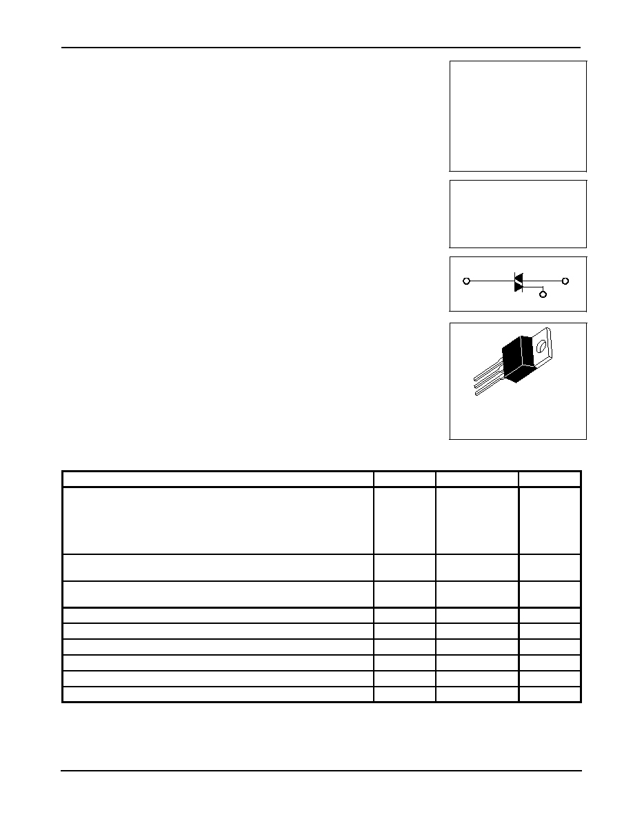
MOTOROLA
SEMICONDUCTOR TECHNICAL DATA
MAC212
Series
MAC212A
Series
CASE 221A-04
(TO-220AB)
STYLE 4
TRIACs
12 AMPERES RMS
200 thru 800 VOLTS
MT1
G
MT2

MAC212 Series MAC212A Series
3ş84
Motorola Thyristor Device Data
THERMAL CHARACTERISTICS
Characteristic
Symbol
Max
Unit
Thermal Resistance, Junction to Case
R
JC
2.1
░
C/W
ELECTRICAL CHARACTERISTICS
(TC = 25
░
C unless otherwise noted.)
Characteristic
Symbol
Min
Typ
Max
Unit
Peak Blocking Current (Either Direction)
(VD = Rated VDRM, Gate Open)
TJ = 25
░
C
TJ = +125
░
C
IDRM
--
--
--
--
10
2
Á
A
mA
Peak On-State Voltage (Either Direction)
ITM = 17 A Peak; Pulse Width = 1 to 2 ms, Duty Cycle
p
2%
VTM
--
1.3
1.75
Volts
Gate Trigger Current (Continuous dc)
(Main Terminal Voltage = 12 Vdc, RL = 100 Ohms)
MT2(+), G(+)
MT2(+), G(ş)
MT2(ş), G(ş)
MT2(ş), G(+) "A" SUFFIX ONLY
IGT
--
--
--
--
12
12
20
35
50
50
50
75
mA
Gate Trigger Voltage (Continuous dc)
(Main Terminal Voltage = 12 Vdc, RL = 100 Ohms)
MT2(+), G(+)
MT2(+), G(ş)
MT2(ş), G(ş)
MT2(ş), G(+) "A" SUFFIX ONLY
(Main Terminal Voltage = Rated VDRM, RL = 10 k
, TJ = +125
░
C)
MT2(+), G(+); MT2(ş), G(ş); MT2(+), G(ş)
MT2(ş), G(+) "A" SUFFIX ONLY
VGT
--
--
--
--
0.2
0.2
0.9
0.9
1.1
1.4
--
--
2
2
2
2.5
--
--
Volts
Holding Current (Either Direction)
(Main Terminal Voltage = 12 Vdc, Gate Open,
Initiating Current = 500 mA)
IH
--
6
50
mA
Turn-On Time
(VD = Rated VDRM, ITM = 17 A, IGT = 120 mA,
Rise Time = 0.1
Á
s, Pulse Width = 2
Á
s)
tgt
--
1.5
--
Á
s
Critical Rate of Rise of Commutation Voltage
(VD = Rated VDRM, ITM = 17 A, Commutating di/dt = 6.1 A/ms,
Gate Unenergized, TC = +85
░
C)
dv/dt(c)
--
5
--
V/
Á
s
Critical Rate of Rise of Off-State Voltage
(VD = Rated VDRM, Exponential Voltage Rise, Gate Open,
TC = +85
░
C)
dv/dt
--
100
--
V/
Á
s
30
░
60
░
90
░
0
4.0
8.0
12
16
20
24
28
14
12
10
6.0
8.0
4.0
2.0
0
IT(RMS), RMS ON-STATE CURRENT (AMP)
115
FIGURE 2 -- POWER DISSIPATION
75
85
95
105
0
2.0
4.0
6.0
8.0
10
12
125
14
IT(RMS), RMS ON-STATE CURRENT (AMP)
dc
180
░
90
░
= CONDUCTION ANGLE
FIGURE 1 -- CURRENT DERATING
60
░
= CONDUCTION ANGLE
T
, MAXIMUM
ALLOW
ABLE CASE
TEMPERA
TURE ( C)
C
░
P
,
A
VERAGE POWER DISSIP
A
TION (W
A
TT)
D(A
V)
= 30
░
dc
= 180
░

MAC212 Series MAC212A Series
3ş85
Motorola Thyristor Device Data
20
100
2.0
50
10
0.2
5.0
1.0
0.5
0.4 0.8 1.2 1.6 2.0 2.4 2.8 3.2 3.6 4.0
0.1
4.4
VT, INSTANTANEOUS ON-STATE VOLTAGE (VOLTS)
FIGURE 3 -- MAXIMUM ON-STATE CHARACTERISTICS
0
20
40
60
80
FIGURE 4 -- MAXIMUM NON-REPETITIVE SURGE CURRENT
100
7.0
1.0
2.0
3.0
5.0
1.6
1.2
0.8
0.4
FIGURE 5 -- TYPICAL GATE TRIGGER VOLTAGE
2.0
CYCLE
TC = 70
░
C
f = 60 Hz
Surge is preceded and followed by rated current
NUMBER OF CYCLES
10
0
80
60
40
20
0
ş20
ş40
ş60
TC, CASE TEMPERATURE (
░
C)
OFF-STATE VOLTAGE = 12 Vdc
ALL MODES
80
60
40
20
0
ş20
ş40
1.2
80
0
0.4
0.8
1.6
ş60
ş60
ş40
ş20
0
20
2.4
40
0
0.4
0.8
1.2
1.6
2.0
2.8
2.0
OFF-STATE VOLTAGE = 12 Vdc
ALL MODES
60
FIGURE 6 -- TYPICAL GATE TRIGGER CURRENT
OFF-STATE VOLTAGE = 12 Vdc
ALL MODES
FIGURE 7 -- TYPICAL HOLDING CURRENT
TC, CASE TEMPERATURE (
░
C)
TC, CASE TEMPERATURE (
░
C)
I T
I , PEAK SURGE CURRENT
(AMP)
TSM
V , GA
TE
TRIGGER VOL
T
AGE (NORMALIZED)
GT
I , HOLDING CURRENT
(NORMALIZED)
H
I , GA
TE
TRIGGER CURRENT
(NORMALIZED)
GT
TJ = 125
░
C
, INST
ANT
ANEOUS ON-ST
A
TE CURRENT
(AMPS)
TJ = 25
░
C

MAC212 Series MAC212A Series
3ş86
Motorola Thyristor Device Data
FIGURE 8 ş THERMAL RESPONSE
r(t),
TRANSIENT
THERMAL
RESIST
ANCE
(NORMALIZED)
10 k
200
5.0 k
2.0 k
1.0 k
500
0.1
t, TIME (ms)
100
50
20
5.0
2.0
1.0
0.02
0.5
1.0
0.5
0.2
0.1
0.05
0.2
0.01
Z
JC(t) = r(t)
Ě
R
JC