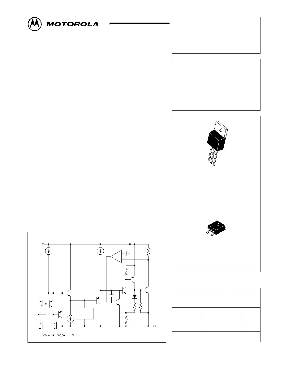
Device
Tested
Operating
Temp.
Range
Package
LT1585A
SILICON MONOLITHIC
INTEGRATED CIRCUIT
5A LOW DROPOUT FAST
RESPONSE POSITIVE
ADJUSTABLE AND FIXED
VOLTAGE REGULATOR
ORDERING INFORMATION
LT1585ACT
0 to 125
°
C
TO220
Order this document by LT1585A/D
T SUFFIX
PLASTIC PACKAGE
CASE 221A
3
1
LT1585ACM
0 to 125
°
C
D2PAK
CM SUFFIX
PLASTIC PACKAGE
CASE 936
(D2PAK)
2
3
1
2
Adjustable output:
Pin 1. Adjust
Pin
2. Vout
Pin
3. Vin
Fixed 1.5V output:
Pin 1. Gnd
Pin
2. Vout
Pin
3. Vin
LT1585ACT1.5 0 to 125
°
C
TO220
Output
Voltage
Type
ADJ.
ADJ.
FIXED
1.5V
LT1585ACM1.5 0 to 125
°
C
D2PAK
FIXED
1.5V
1
MOTOROLA ANALOG IC DEVICE DATA
5A Low Dropout Fast Response
Positive Adjustable and Fixed
Voltage Regulators
The LT1585A is a low dropout 3terminal voltage regulator with 5A output
current capability.
Design has been optimized for low voltage applications where transient
response and minimum input voltage are critical. This voltage regulator
features a low dropout voltage and fast transient response. These
improvements make them ideal for low voltage microprocessor applications
requiring a regulated 2.5V to 3.6V output with an input supply below 7V.
Current limits is trimmed to ensure specified output current and controlled
shortcircuit current. Onchip thermal limiting provides protection against
any combination of overload that would create excessive junction
temperatures. The LT1585A is available in the industry standard 3pin
TO220 and D2PAK power package.
Features
·
Fast Transient Response
·
Guaranteed Dropout Voltage at Multiple Currents
·
Load Regulation: 0.05% Typ
·
Trimmed Current Limit
·
OnChip Thermal Limiting
·
Standard 3Pin Power Package
Applications
·
Pentium
®
Processor Supplies
·
Power PC
TM
Supplies
·
Other 2.5V to 3.6V Microprocessor Supplies
·
Low Voltage Logic Supplies
·
BatteryPowered Circuitry
·
Post Regulator for Switching Supply
Simplified Block Diagram
Vin
Vout
+
Thermal
Limit
Adjust
©
Motorola, Inc. 1999
Rev 0
LT1585A
2
MOTOROLA ANALOG IC DEVICE DATA
ABSOLUTE MAXIMUM RATINGS
(
Absolute Maximum Ratings indicate limits beyond which damage to the device may occur)
Rating
Symbol
Pin #
Value
Unit
ÁÁÁÁÁÁÁÁÁÁÁÁÁÁÁÁÁÁÁ
ÁÁÁÁÁÁÁÁÁÁÁÁÁÁÁÁÁÁÁ
Maximum Supply Voltage
ÁÁÁÁÁ
ÁÁÁÁÁ
Vin
ÁÁÁ
ÁÁÁ
3
ÁÁÁÁÁÁÁÁ
ÁÁÁÁÁÁÁÁ
12
ÁÁÁ
ÁÁÁ
V
ÁÁÁÁÁÁÁÁÁÁÁÁÁÁÁÁÁÁÁ
ÁÁÁÁÁÁÁÁÁÁÁÁÁÁÁÁÁÁÁ
Power Dissipation
ÁÁÁÁÁ
ÁÁÁÁÁ
ÁÁÁ
ÁÁÁ
ÁÁÁÁÁÁÁÁ
ÁÁÁÁÁÁÁÁ
ÁÁÁ
ÁÁÁ
Case 221A (TO220) (TJ = +25
°
C)
PD
Internally Limited
W
Thermal Resistance, JunctiontoAmbient
R
JA
65
°
C/W
Thermal Resistance, JunctiontoCase
R
JC
5.0
°
C/W
Case 936 (D2PAK) (TJ = +25
°
C)
PD
Internally Limited
W
Thermal Resistance, JunctiontoAmbient
R
JA
70
°
C/W
Thermal Resistance, JunctiontoCase
R
JC
5.0
°
C/W
ÁÁÁÁÁÁÁÁÁÁÁÁÁÁÁÁÁÁÁ
ÁÁÁÁÁÁÁÁÁÁÁÁÁÁÁÁÁÁÁ
Storage Temperature Range
ÁÁÁÁÁ
ÁÁÁÁÁ
Tstg
ÁÁÁ
ÁÁÁ
ÁÁÁÁÁÁÁÁ
ÁÁÁÁÁÁÁÁ
65 to 150
ÁÁÁ
ÁÁÁ
°
C
ÁÁÁÁÁÁÁÁÁÁÁÁÁÁÁÁÁÁÁ
Minimum ESD Rating (Human Body Model: C = 100pF, R = 1.5 k
W
)
ÁÁÁÁÁ
ÁÁÁ
ÁÁÁÁÁÁÁÁ
3.0
ÁÁÁ
kV
ÁÁÁÁÁÁÁÁÁÁÁÁÁÁÁÁÁÁÁ
ÁÁÁÁÁÁÁÁÁÁÁÁÁÁÁÁÁÁÁ
Lead Temperature (Soldering, 10 sec.)
ÁÁÁÁÁ
ÁÁÁÁÁ
ÁÁÁ
ÁÁÁ
ÁÁÁÁÁÁÁÁ
ÁÁÁÁÁÁÁÁ
260
ÁÁÁ
ÁÁÁ
°
C
ÁÁÁÁÁÁÁÁÁÁÁÁÁÁÁÁÁÁÁ
ÁÁÁÁÁÁÁÁÁÁÁÁÁÁÁÁÁÁÁ
Maximum Junction Temperature
ÁÁÁÁÁ
ÁÁÁÁÁ
TJ
ÁÁÁ
ÁÁÁ
ÁÁÁÁÁÁÁÁ
ÁÁÁÁÁÁÁÁ
150
ÁÁÁ
ÁÁÁ
°
C
OPERATING RATINGS
(Operating Ratings indicate conditions for which the device is intended to be functional, but do not guarantee
specific performance limits. For guaranteed specifications and test conditions, see the Electrical Characteristics)
Rating
Symbol
Pin #
Value
Unit
ÁÁÁÁÁÁÁÁÁÁÁÁÁÁÁÁÁÁÁ
ÁÁÁÁÁÁÁÁÁÁÁÁÁÁÁÁÁÁÁ
Operating Junction Temperature Range
ÁÁÁÁÁ
ÁÁÁÁÁ
TJ
ÁÁÁ
ÁÁÁ
ÁÁÁÁÁÁÁÁ
ÁÁÁÁÁÁÁÁ
0 to +125
ÁÁÁ
ÁÁÁ
°
C
ÁÁÁÁÁÁÁÁÁÁÁÁÁÁÁÁÁÁÁ
Á
ÁÁÁÁÁÁÁÁÁÁÁÁÁÁÁÁÁ
Á
ÁÁÁÁÁÁÁÁÁÁÁÁÁÁÁÁÁÁÁ
Supply Voltage
ÁÁÁÁÁ
Á
ÁÁÁ
Á
ÁÁÁÁÁ
ÁÁÁ
Á
ÁÁ
ÁÁÁ
3
ÁÁÁÁÁÁÁÁ
Á
ÁÁÁÁÁÁ
Á
ÁÁÁÁÁÁÁÁ
7.0
ÁÁÁ
Á
Á
Á
ÁÁÁ
V
ELECTRICAL CHARACTERISTICS
(0 < TJ < +125
°
C, unless otherwise noted)
Characteristic
Symbol
Pin #
Min
Typ
Max
Unit
ÁÁÁÁÁÁÁÁÁÁÁÁÁÁÁÁÁÁÁ
ÁÁÁÁÁÁÁÁÁÁÁÁÁÁÁÁÁÁÁ
Reference Voltage (LT1585A)
ÁÁÁÁÁ
ÁÁÁÁÁ
Vref
ÁÁÁ
ÁÁÁ
1
ÁÁÁ
ÁÁÁ
ÁÁÁÁ
ÁÁÁÁ
ÁÁÁ
ÁÁÁ
ÁÁÁ
ÁÁÁ
V
(VinVout) = 3V, Iout = 10mA, TJ = 25
°
C
1.238
1.250
1.262
1.5V
(VinVout)
5.75V, 10mA
Iout
5A
1.225
1.250
1.275
ÁÁÁÁÁÁÁÁÁÁÁÁÁÁÁÁÁÁÁ
ÁÁÁÁÁÁÁÁÁÁÁÁÁÁÁÁÁÁÁ
Output Voltage (LT1585A1.5)
ÁÁÁÁÁ
ÁÁÁÁÁ
ÁÁÁ
ÁÁÁ
2
ÁÁÁ
ÁÁÁ
ÁÁÁÁ
ÁÁÁÁ
ÁÁÁ
ÁÁÁ
ÁÁÁ
ÁÁÁ
V
Vin = 5V, TJ = 25
°
C, Iout = 0mA
1.485
1.5
1.515
3V
Vin
7V, 0mA
Iout
5A
1.470
1.5
1.530
ÁÁÁÁÁÁÁÁÁÁÁÁÁÁÁÁÁÁÁ
ÁÁÁÁÁÁÁÁÁÁÁÁÁÁÁÁÁÁÁ
Line Regulation [Notes 1, 2]
ÁÁÁÁÁ
ÁÁÁÁÁ
Regline
ÁÁÁ
ÁÁÁ
2
ÁÁÁ
ÁÁÁ
ÁÁÁÁ
ÁÁÁÁ
ÁÁÁ
ÁÁÁ
ÁÁÁ
ÁÁÁ
%
LT1585A: 2.75V
Vin
7V, Iout = 10mA
0.005
0.2
LT1585A1.5: 3V
Vin
7V, Iout = 0mA
0.005
0.2
ÁÁÁÁÁÁÁÁÁÁÁÁÁÁÁÁÁÁÁ
ÁÁÁÁÁÁÁÁÁÁÁÁÁÁÁÁÁÁÁ
Load Regulation [Notes 1, 2]
ÁÁÁÁÁ
ÁÁÁÁÁ
Regload
ÁÁÁ
ÁÁÁ
2
ÁÁÁ
ÁÁÁ
ÁÁÁÁ
ÁÁÁÁ
ÁÁÁ
ÁÁÁ
ÁÁÁ
ÁÁÁ
%
LT1585A: (VinVout) = 3V, TJ = 25
°
C, 10mA
Iout
5A
0.05
0.3
LT1585A1.5: Vin = 5V, TJ = 25
°
C, 0mA
Iout
5A
0.05
0.3
LT1585A: (VinVout) = 3V, 10mA
Iout
5A
0.05
0.5
LT1585A1.5: Vin = 5V, 0mA
Iout
5A
0.05
0.5
ÁÁÁÁÁÁÁÁÁÁÁÁÁÁÁÁÁÁÁ
ÁÁÁÁÁÁÁÁÁÁÁÁÁÁÁÁÁÁÁ
Dropout Voltage
ÁÁÁÁÁ
ÁÁÁÁÁ
VinVout
ÁÁÁ
ÁÁÁ
ÁÁÁ
ÁÁÁ
ÁÁÁÁ
ÁÁÁÁ
ÁÁÁ
ÁÁÁ
ÁÁÁ
ÁÁÁ
V
LT1585A:
D
VREF = 1%, IOUT = 3A
1.150
1.300
LT1585A1.5:
D
VOUT = 1%, IOUT = 3A
1.150
1.300
LT1585A:
D
VREF = 1%, IOUT = 5A
1.200
1.400
LT1585A1.5:
D
VOUT = 1%, IOUT = 5A
1.200
1.400
ÁÁÁÁÁÁÁÁÁÁÁÁÁÁÁÁÁÁÁ
ÁÁÁÁÁÁÁÁÁÁÁÁÁÁÁÁÁÁÁ
Current Limit [Note 3]
ÁÁÁÁÁ
ÁÁÁÁÁ
ILimit
ÁÁÁ
ÁÁÁ
2
ÁÁÁ
ÁÁÁ
ÁÁÁÁ
ÁÁÁÁ
ÁÁÁ
ÁÁÁ
ÁÁÁ
ÁÁÁ
A
(VinVout) = 5.5V
5.0
6.0
ÁÁÁÁÁÁÁÁÁÁÁÁÁÁÁÁÁÁÁ
ÁÁÁÁÁÁÁÁÁÁÁÁÁÁÁÁÁÁÁ
Adjust Pin Current (LT1585A)
ÁÁÁÁÁ
ÁÁÁÁÁ
IAdj
ÁÁÁ
ÁÁÁ
1
ÁÁÁ
ÁÁÁ
ÁÁÁÁ
ÁÁÁÁ
55
ÁÁÁ
ÁÁÁ
120
ÁÁÁ
ÁÁÁ
µ
A
ÁÁÁÁÁÁÁÁÁÁÁÁÁÁÁÁÁÁÁ
ÁÁÁÁÁÁÁÁÁÁÁÁÁÁÁÁÁÁÁ
Adjust Pin Current Change (LT1585A) [Note 3]
ÁÁÁÁÁ
ÁÁÁÁÁ
ÁÁÁ
ÁÁÁ
1
ÁÁÁ
ÁÁÁ
ÁÁÁÁ
ÁÁÁÁ
ÁÁÁ
ÁÁÁ
ÁÁÁ
ÁÁÁ
µ
A
1.5V
(VinVout)
5.75V, 10mA
Iout
5A
0.2
5.0
ÁÁÁÁÁÁÁÁÁÁÁÁÁÁÁÁÁÁÁ
Minimum Load Current (LT1585A) 1.5V
(VinVout)
5.75V
ÁÁÁÁÁ
ILoad min
ÁÁÁ
2
ÁÁÁ
ÁÁÁÁ
2.0
ÁÁÁ
10
ÁÁÁ
mA
ÁÁÁÁÁÁÁÁÁÁÁÁÁÁÁÁÁÁÁ
ÁÁÁÁÁÁÁÁÁÁÁÁÁÁÁÁÁÁÁ
Quiescent Current (LT1585A1.5) Vin = 5V
ÁÁÁÁÁ
ÁÁÁÁÁ
ÁÁÁ
ÁÁÁ
1
ÁÁÁ
ÁÁÁ
ÁÁÁÁ
ÁÁÁÁ
7.0
ÁÁÁ
ÁÁÁ
13
ÁÁÁ
ÁÁÁ
mA
ÁÁÁÁÁÁÁÁÁÁÁÁÁÁÁÁÁÁÁ
ÁÁÁÁÁÁÁÁÁÁÁÁÁÁÁÁÁÁÁ
Ripple Rejection
ÁÁÁÁÁ
ÁÁÁÁÁ
RR
ÁÁÁ
ÁÁÁ
2
ÁÁÁ
ÁÁÁ
ÁÁÁÁ
ÁÁÁÁ
ÁÁÁ
ÁÁÁ
ÁÁÁ
ÁÁÁ
dB
LT1585A: f = 120Hz, Cout = 25
µ
F Tant., (VinVout) = 3V, Iout = 5A
60
72
LT1585A1.5: f = 120Hz, Cout = 25
µ
F Tant., Vin = 4.5V, Iout = 5A
60
72
ÁÁÁÁÁÁÁÁÁÁÁÁÁÁÁÁÁÁÁ
Thermal Regulation TJ = 25
°
C, 30ms Pulse
ÁÁÁÁÁ
T
°
Reg
ÁÁÁ
ÁÁÁ
ÁÁÁÁ
0.004
ÁÁÁ
ÁÁÁ
%/W
ÁÁÁÁÁÁÁÁÁÁÁÁÁÁÁÁÁÁÁ
ÁÁÁÁÁÁÁÁÁÁÁÁÁÁÁÁÁÁÁ
Temperature Stability
ÁÁÁÁÁ
ÁÁÁÁÁ
T
°
Stab
ÁÁÁ
ÁÁÁ
ÁÁÁ
ÁÁÁ
ÁÁÁÁ
ÁÁÁÁ
0.5
ÁÁÁ
ÁÁÁ
ÁÁÁ
ÁÁÁ
%
ÁÁÁÁÁÁÁÁÁÁÁÁÁÁÁÁÁÁÁ
ÁÁÁÁÁÁÁÁÁÁÁÁÁÁÁÁÁÁÁ
Long Term Stability TJ = 125
°
C, 1000 Hrs
ÁÁÁÁÁ
ÁÁÁÁÁ
ÁÁÁ
ÁÁÁ
ÁÁÁ
ÁÁÁ
ÁÁÁÁ
ÁÁÁÁ
0.03
ÁÁÁ
ÁÁÁ
1.0
ÁÁÁ
ÁÁÁ
%
ÁÁÁÁÁÁÁÁÁÁÁÁÁÁÁÁÁÁÁ
ÁÁÁÁÁÁÁÁÁÁÁÁÁÁÁÁÁÁÁ
RMS Output Noise (% of Vout) TJ = 25
°
C, 10Hz
f
10kHz
ÁÁÁÁÁ
ÁÁÁÁÁ
ÁÁÁ
ÁÁÁ
ÁÁÁ
ÁÁÁ
ÁÁÁÁ
ÁÁÁÁ
0.003
ÁÁÁ
ÁÁÁ
ÁÁÁ
ÁÁÁ
%
NOTES 1. See thermal regulation specifications for changes in output voltage due to heating effects. Load and line regulation are measured at a constant
junction temperature by low duty cycle pulse testing.
2. Line and load regulations are guaranteed up to the maximum power dissipation 28.8W for the LT1585A in Tpackage. Power dissipation is
determined by input/output differential and the output current. Guaranteed maximum output power will not be available over the full input/output voltage range.
3. The LT1585A has constant current limit with changes in inputtooutput voltage.

LT1585A
3
MOTOROLA ANALOG IC DEVICE DATA
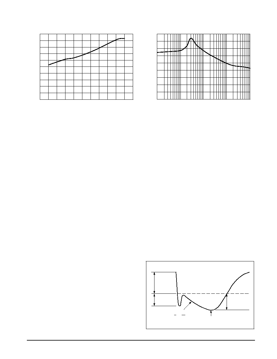
Figure 1. Dropout Voltage vs Output Current
Figure 2. ShortCircuit Current vs Temperature
Figure 3. Load Regulation vs Temperature
DROPOUT
VOL
T
AGE
(V)
0
2.0
6.0
0.5
OUTPUT CURRENT (A)
4.0
0.6
0.8
0.7
5
°
C
Figure 4. LT1585A Reference Voltage vs
Temperature
Figure 5. LT1585A1.5 Output Voltage vs
Temperature
Figure 6. LT1585A1.5 Quiescent Current vs
Temperature
0.9
1.0
1.1
1.3
1.2
1.4
1.0
3.0
5.0
V
40
60
20
160
1.225
TEMPERATURE (
°
C)
40
100
1.23
1.235
1.245
1.24
1.25
1.255
1.26
1.27
1.265
1.275
0
20
60
80
140
120
(V)
ref
V
40
60
20
1.485
TEMPERATURE (
°
C)
40
100
1.49
1.495
1.5
1.505
1.51
1.515
0
20
60
80
140
120
(V)
out
I
40
60
20
140
5.0
TEMPERATURE (
°
C)
40
100
5.2
5.4
5.8
5.6
6.0
6.2
6.4
6.8
6.6
7.0
0
20
60
80
120
(A)
sc
LOAD REGULA
TION
(%)
40
60
20
0.2
TEMPERATURE (
°
C)
40
100
0.15
0.1
0.05
0
0.05
0.1
0
20
60
80
140
120
25
°
C
125
°
C
I
40
60
20
5.0
TEMPERATURE (
°
C)
40
100
5.5
6.0
7.0
6.5
7.5
8.0
8.5
9.5
9.0
10
0
20
60
80
140
120
(mA)
q
LT1585A
4
MOTOROLA ANALOG IC DEVICE DATA
Figure 7. LT1585A Adjust Pin Current vs
Temperature
Figure 8. Ripple Rejection vs Frequency
V
10
100,000
0
TEMPERATURE (
°
C)
10,000
10
20
30
40
50
60
80
70
90
100
1000
(V)
ref
I
40
60
20
160
0
TEMPERATURE (
°
C)
40
100
10
20
40
30
50
60
70
90
80
100
0
20
60
80
140
120
(
A)
adj
m
OPERATING DESCRIPTION
APPLICATIONS INFORMATION
General
The LT1585A 3terminal adjustable positive voltage
regulator is easy to use and has all the protection features
expected in high performance linear regulators. The device is
shortcircuit protected, safearea protected and provides
thermal shutdown to turn off the regulator should the junction
temperature exceed about 150
°
C.
The LT1585A voltage regulator requires an output
capacitor for stability. However, the improved frequency
compensation permits the use of capacitors with much lower
ESR while still maintaining stability. This is critical in
addressing the needs of modern, low voltage, high speed
microprocessors.
Current generation microprocessors cycle load current
from almost zero to amps in tens of nanoseconds. Output
voltage tolerances are tighter and include transient response
as part of the specification.
The LT1585A is specifically designed to meet the fast
current loadstep requirements of these microprocessors
and save total cost by needing less output capacitance in
order to maintain regulation.
Stability
The circuit design in the LT1585A requires the use of an
output capacitor as part of the frequency compensation. For
all operating conditions, the addition of a 22
µ
F solid tantalum
or a 100
µ
F aluminium electrolytic on the output ensures
stability. Normally, the LT1585A can use smaller value
capacitors. Many different types of capacitors are available
and have widely varying characteristics.
These capacitors differ in capacitor tolerance (sometimes
ranging up to
±
100%), equivalent series resistance,
equivalent series inductance and capacitance temperature
coefficient. The LT1585A frequency compensation optimizes
frequency response with low ESR capacitors. In general, use
capacitors with an ESR of less than 1
.
On the LT1585A, bypassing the adjust pin improves ripple
rejection and transient response. Bypassing the adjust pin
increases the required output capacitor value. The value of
22
µ
F tantalum or 100
µ
F aluminium covers all cases of
bypassing the adjust terminal. With no adjust pin bypassing,
smaller values of capacitors provide equally good results.
Normally, capacitor values on the order of several hundred
microfarads are used on the output of the regulators to
ensure good transient response with heavy load current
changes.
Output capacitance can increase without limit and larger
values of output capacitance further improve the stability and
transient response of the LT1585A.
Large load current changes are exactly the situation
presented by modern microprocessors. The load current step
contains higher order frequency components that the output
decoupling network must handle until the regulator throttles
to the load current level. Capacitors are not ideal elements
and contain parasitic resistance and inductance. These
parasitic elements dominate the change in output voltage at
the beginning of a transient load step change.
The ESR of the output capacitors produces an
instantaneous step in output voltage (
V =
I
·
ESR). The
ESL of the output capacitors produces a droop proportional
to the rate of change of output current (V = L
·
I/
t). The
output capacitance produces a change in output voltage
proportional to the time until the regulator can respond (
V =
t
·
l/C). These transient effects are illustrated in Figure 9.
Figure 9.
ESR
Effects
ESL
Effects
Capacitance
Effects
Slope, V
t
+ D
I
C
Point at which
Regulator Takes Control
LT1585A
5
MOTOROLA ANALOG IC DEVICE DATA
The use of capacitors with low ESR, low ESL and good
high frequency characteristics is critical in meeting the output
voltage tolerances of these high speed microprocessors.
These requirements dictate a combination of high quality,
surface mount tantalum capacitors and ceramic capacitors.
The location of the decoupling network is critical to
transient response performance. Place the decoupling
network as close as possible to the processor pins because
trace runs from the decoupling capacitors to the processor
pins are inductive. The ideal location for the decoupling
network is actually inside the microprocessor socket cavity.
In addition, use large power and ground plane areas to
minimize distribution drops.
A possible stability problem that occurs in monolithic linear
regulators is current limit oscillations. The LT1585A
essentially has a flat current limit over the range of input
supply voltage. The lower current limit rating and 12V
maximum supply voltage rating for these devices permit this
characteristic.
Current limit oscillations are typically nonexistent, unless
the input and output decoupling capacitors for the regulators
are mounted several inches from the terminals.
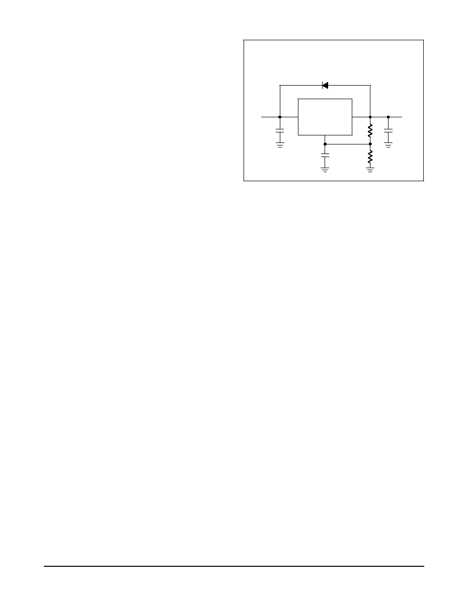
Protection Diodes
In normal operation, the LT1585A does not require any
protection diodes. Older 3terminal regulators require
protection diodes between the output pin and the input pin or
between the adjust pin and the output pin to prevent die
overstress.
Builtin internal resistors limit internal current paths on the
adjust pin. Therefore, even with bypass capacitors on the
adjust pin, no protection diode is needed to ensure device
safety under shortcircuit conditions.
A protection diode between the input and output pins is
usually not needed. An internal diode between the input and
output pins on the LT1585A can handle microsecond surge
currents of 50A to 100A. Even with large value output
capacitors it is difficult to obtain those values of surge
currents in normal operation. Only with large values of output
capacitance, such as 1000
µ
F to 500
µ
F, and with the input pin
instantaneously shorted to ground can damage occur. A
crowbar circuit at the input of the LT1585A can generate
those levels of current, and a diode from output to input is
then recommended. This is shown in Figure 10. Usually,
normal power supply cycling or system "hot plugging and
unplugging" will not generate current large enough to do any
damage.
The adjust pin can be driven on a transient basis
±
7V with
respect to the output, without any device degradation. As
w i t h a n y I C r e g u l a t o r, e x c e e d i n g t h e m a x i m u m
inputtooutput voltage differential causes the internal
transistors to break down and none of the protection circuitry
is then functional.
Vout
Vin
LT1585A
ADJ
IN
OUT
D1
1N4002
(Optional)
+
+
+
R2
R1
C2
10
m
F
C1
10
m
F
C
Figure 10.
Ripple Rejection
A bypass capacitor from the adjust pin to ground reduces
the output ripple by the ratio of VOUT
/1.25 V. The impedance
of the adjust pin capacitor at the ripple frequency should be
less than the value of R1 (typically in the rage of 100
to
120
) in the feedback divider network in Figure 10.
Therefore, the value of the required adjust pin capacitor is a
function of the input ripple frequency. For example, if R1
equals 100
and the ripple frequency equals 120Hz, the
adjust pin capacitor should be 22
µ
F. At 10kHz, only 0.22
µ
F is
needed.
Output Voltage
The LT1585A adjustable regulator develops a 1.25V
reference voltage between the output pin and the adjust pin
(see Figure 11). Placing a resistor R1 between these two
terminals causes a constant current to flow through R1 and
down through R2 to set the overall output voltage. Normally,
this current is the specified minimum load current of 10mA.
The current out of the adjust pin adds to the current from R1
and is typically 55
µ
A. Its output voltage contribution is small
and only needs consideration when very precise output
voltage setting is required.