Äîêóìåíòàöèÿ è îïèñàíèÿ www.docs.chipfind.ru
©
Motorola, Inc. 1997
Logic Level TMOS
NChannel Enhancement Mode
This TMOS FET is designed for high voltage, high speed
switching applications such as line drivers, relay drivers, CMOS
logic, microprocessor or TTL to high voltage interface and high
voltage display drivers.
·
Low Drive Requirement, VGS = 3.0 V max
·
Inherent Current Sharing Capability Permits Easy Paralleling of
many Devices
MAXIMUM RATINGS
Rating
Symbol
Value
Unit
Drain Source Voltage
VDSS
200
Vdc
GateSource Voltage
VGS
±
20
Vdc
Drain Current
Continuous(1)
Pulsed(2)
ID
IDM
250
500
mAdc
Total Power Dissipation
@ TA = 25
°
C
Derate above TA = 25
°
C
PD
350
6.4
mW
mW/
°
C
Operating and Storage Temperature Range
TJ, Tstg
55 to +150
°
C
1. The Power Dissipation of the package may result in a lower continuous drain current.
2. Pulse Test: Pulse Width
v
300
µ
s, Duty Cycle
v
2.0%.
TMOS is a registered trademark of Motorola, Inc.
Order this document
by BS108/D
MOTOROLA
SEMICONDUCTOR TECHNICAL DATA
BS108
200 VOLTS
NCHANNEL TMOS
POWER FET
LOGIC LEVEL
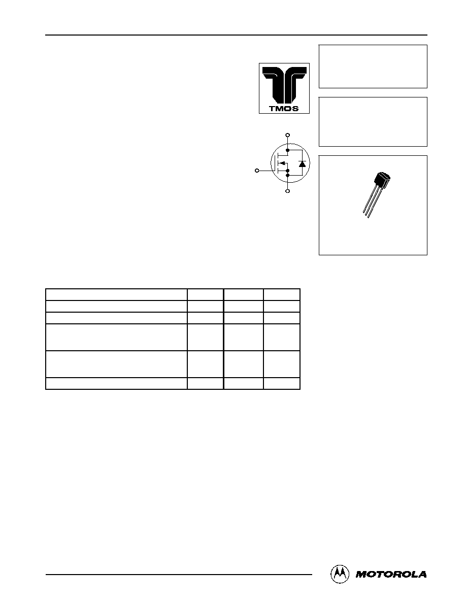
CASE 2904, STYLE 30
TO92
1
2
3
®
1 DRAIN
2
GATE
3 SOURCE
BS108
2
Motorola SmallSignal Transistors, FETs and Diodes Device Data
ELECTRICAL CHARACTERISTICS
(TA = 25
°
C unless otherwise noted)
Characteristic
Symbol
Min
Typ
Max
Unit
OFF CHARACTERISTICS
DrainSource Breakdown Voltage
(VGS = 0, ID = 10
µ
A)
V(BR)DSS
200
--
--
Vdc
Zero Gate Voltage Drain Current
(VDSS = 130 Vdc, VGS = 0)
IDSS
--
--
30
nAdc
GateBody Leakage Current
(VGS = 15 Vdc, VDS = 0)
IGSSF
--
--
10
nAdc
ON CHARACTERISTICS (2)
Gate Threshold Voltage
(ID = 1.0 mA, VDS = VGS)
VGS(th)
0.5
--
1.5
Vdc
Static DraintoSource OnResistance
(VGS = 2.0 Vdc, ID = 50 mA)
(VGS = 2.8 Vdc, ID = 100 mA)
rDS(on)
--
--
--
--
10
8.0
Ohms
Drain Cutoff Current
(VGS = 0.2 V, VDS = 70 V)
IDSX
--
--
25
m
A
DYNAMIC CHARACTERISTICS
Input Capacitance
(VDS = 25 V, VGS = 0, f = 1.0 MHz)
Ciss
--
--
150
pF
Output Capacitance
(VDS = 25 V, VGS = 0, f = 1.0 MHz)
Coss
--
--
30
pF
Reverse Transfer Capacitance
(VDS = 25 V, VGS = 0, f = 1.0 MHz)
Crss
--
--
10
pF
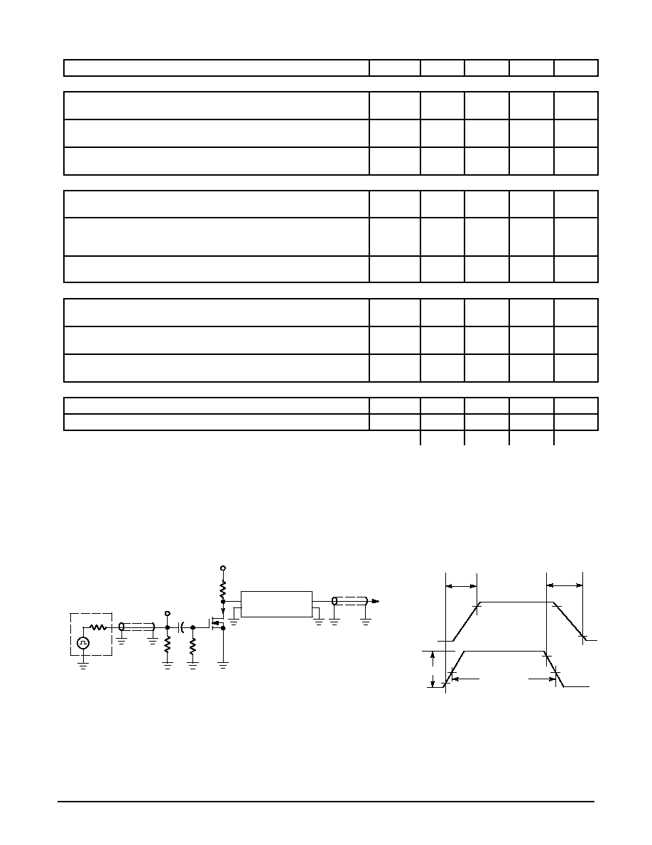
SWITCHING CHARACTERISTICS
TurnOn Time (See Figure 1)
td(on)
--
--
15
ns
TurnOff Time (See Figure 1)
td(off)
--
--
15
ns
2. Pulse Test: Pulse Width
300
µ
s, Duty Cycle = 2.0%.
Figure 1. Switching Test Circuit
Figure 2. Switching Waveforms
RESISTIVE SWITCHING
OUTPUT
INVERTED
50%
10%
50%
toff
ton
Vin
Vout
PULSE
WIDTH
90%
10%
INPUT
90%
90%
10 V
20 dB
50
ATTENUATOR
PULSE GENERATOR
+25 V
Vin
40 pF
1.0 M
50
23
50
Vout
TO SAMPLING SCOPE
50
INPUT
BS108
3
Motorola SmallSignal Transistors, FETs and Diodes Device Data
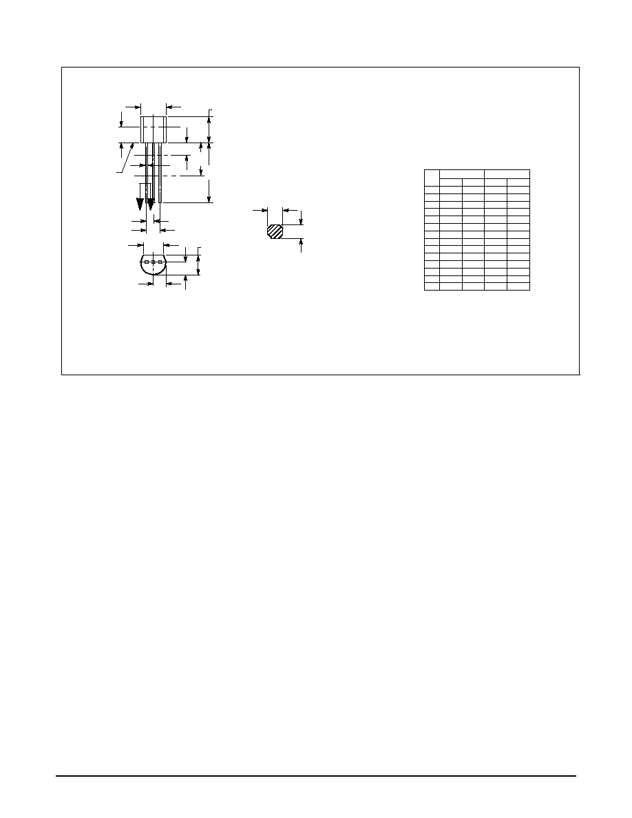
PACKAGE DIMENSIONS
CASE 02904
(TO226AA)
ISSUE AD
NOTES:
1. DIMENSIONING AND TOLERANCING PER ANSI
Y14.5M, 1982.
2. CONTROLLING DIMENSION: INCH.
3. CONTOUR OF PACKAGE BEYOND DIMENSION R
IS UNCONTROLLED.
4. DIMENSION F APPLIES BETWEEN P AND L.
DIMENSION D AND J APPLY BETWEEN L AND K
MINIMUM. LEAD DIMENSION IS UNCONTROLLED
IN P AND BEYOND DIMENSION K MINIMUM.
R
A
P
J
L
F
B
K
G
H
SECTION XX
C
V
D
N
N
X X
SEATING
PLANE
DIM
MIN
MAX
MIN
MAX
MILLIMETERS
INCHES
A
0.175
0.205
4.45
5.20
B
0.170
0.210
4.32
5.33
C
0.125
0.165
3.18
4.19
D
0.016
0.022
0.41
0.55
F
0.016
0.019
0.41
0.48
G
0.045
0.055
1.15
1.39
H
0.095
0.105
2.42
2.66
J
0.015
0.020
0.39
0.50
K
0.500
12.70
L
0.250
6.35
N
0.080
0.105
2.04
2.66
P
0.100
2.54
R
0.115
2.93
V
0.135
3.43
1
STYLE 30:
PIN 1. DRAIN
2. GATE
3. SOURCE

BS108
4
Motorola SmallSignal Transistors, FETs and Diodes Device Data
Motorola reserves the right to make changes without further notice to any products herein. Motorola makes no warranty, representation or guarantee regarding
the suitability of its products for any particular purpose, nor does Motorola assume any liability arising out of the application or use of any product or circuit, and
specifically disclaims any and all liability, including without limitation consequential or incidental damages. "Typical" parameters which may be provided in Motorola
data sheets and/or specifications can and do vary in different applications and actual performance may vary over time. All operating parameters, including "Typicals"
must be validated for each customer application by customer's technical experts. Motorola does not convey any license under its patent rights nor the rights of
others. Motorola products are not designed, intended, or authorized for use as components in systems intended for surgical implant into the body, or other
applications intended to support or sustain life, or for any other application in which the failure of the Motorola product could create a situation where personal injury
or death may occur. Should Buyer purchase or use Motorola products for any such unintended or unauthorized application, Buyer shall indemnify and hold Motorola
and its officers, employees, subsidiaries, affiliates, and distributors harmless against all claims, costs, damages, and expenses, and reasonable attorney fees
arising out of, directly or indirectly, any claim of personal injury or death associated with such unintended or unauthorized use, even if such claim alleges that
Motorola was negligent regarding the design or manufacture of the part. Motorola and are registered trademarks of Motorola, Inc. Motorola, Inc. is an Equal
Opportunity/Affirmative Action Employer.
Mfax is a trademark of Motorola, Inc.
How to reach us:
USA / EUROPE / Locations Not Listed: Motorola Literature Distribution;
JAPAN: Nippon Motorola Ltd.; TatsumiSPDJLDC, 6F SeibuButsuryuCenter,
P.O. Box 5405, Denver, Colorado 80217. 3036752140 or 18004412447
3142 Tatsumi KotoKu, Tokyo 135, Japan. 81335218315
Mfax
TM
: RMFAX0@email.sps.mot.com TOUCHTONE 6022446609
ASIA/PACIFIC: Motorola Semiconductors H.K. Ltd.; 8B Tai Ping Industrial Park,
INTERNET: http://DesignNET.com
51 Ting Kok Road, Tai Po, N.T., Hong Kong. 85226629298
BS108/D