Äîêóìåíòàöèÿ è îïèñàíèÿ www.docs.chipfind.ru
1
Motorola SmallSignal Transistors, FETs and Diodes Device Data
Preliminary Information
NPN Silicon General Purpose
Amplifier Transistor
This NPN transistor is designed for general purpose amplifier applications.
This device is housed in the SOT-416/SC90 package which is designed for
low power surface mount applications, where board space is at a premium.
·
Reduces Board Space
·
High hFE, 210460 (typical)
·
Low VCE(sat), < 0.5 V
·
Available in 8 mm, 7-inch/3000 Unit Tape and Reel
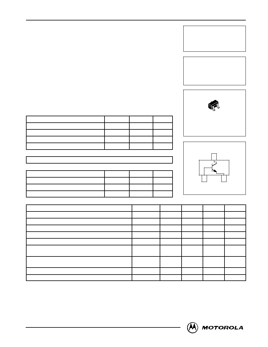
MAXIMUM RATINGS
(TA = 25
°
C)
Rating
Symbol
Value
Unit
Collector-Base Voltage
V(BR)CBO
50
Vdc
Collector-Emitter Voltage
V(BR)CEO
50
Vdc
Emitter-Base Voltage
V(BR)EBO
5.0
Vdc
Collector Current -- Continuous
IC
100
mAdc
DEVICE MARKING
2SC4617 = B9
THERMAL CHARACTERISTICS
Rating
Symbol
Max
Unit
Power Dissipation(1)
PD
125
mW
Junction Temperature
TJ
150
°
C
Storage Temperature Range
Tstg
55 ~ + 150
°
C
ELECTRICAL CHARACTERISTICS
(TA = 25
°
C)
Characteristic
Symbol
Min
Typ
Max
Unit
Collector-Base Breakdown Voltage (IC = 50
µ
Adc, IE = 0)
V(BR)CBO
50
--
--
Vdc
Collector-Emitter Breakdown Voltage (IC = 1.0 mAdc, IB = 0)
V(BR)CEO
50
--
--
Vdc
Emitter-Base Breakdown Voltage (IE = 50
µ
Adc, IE = 0)
V(BR)EBO
5.0
--
--
Vdc
Collector-Base Cutoff Current (VCB = 30 Vdc, IE = 0)
ICBO
--
--
0.5
µ
A
Emitter-Base Cutoff Current (VEB = 4.0 Vdc, IB = 0)
IEBO
--
--
0.5
µ
A
Collector-Emitter Saturation Voltage(2)
(IC = 60 mAdc, IB = 5.0 mAdc)
VCE(sat)
--
--
0.4
Vdc
DC Current Gain(2)
(VCE = 6.0 Vdc, IC = 1.0 mAdc)
hFE
120
--
560
--
Transition Frequency (VCE = 12 Vdc, IC = 2.0 mAdc, f = 30 MHz)
fT
--
180
--
MHz
Output Capacitance (VCB = 12 Vdc, IC = 0 Adc, f = 1 MHz)
COB
--
2.0
--
pF
1. Device mounted on a FR-4 glass epoxy printed circuit board using the minimum recommended footprint.
2. Pulse Test: Pulse Width
300
µ
s, D.C.
2%.
This document contains information on a product under development. Motorola reserves the right to change or discontinue this product without notice.
Thermal Clad is a trademark of the Bergquist Company
Order this document
by 2SC4617/D
MOTOROLA
SEMICONDUCTOR TECHNICAL DATA
2SC4617
NPN GENERAL
PURPOSE AMPLIFIER
TRANSISTORS
SURFACE MOUNT
CASE 46301, STYLE 1
SOT416/SC90
1
2
3
COLLECTOR
3
1
BASE
2
EMITTER
©
Motorola, Inc. 1996
2SC4617
2
Motorola SmallSignal Transistors, FETs and Diodes Device Data
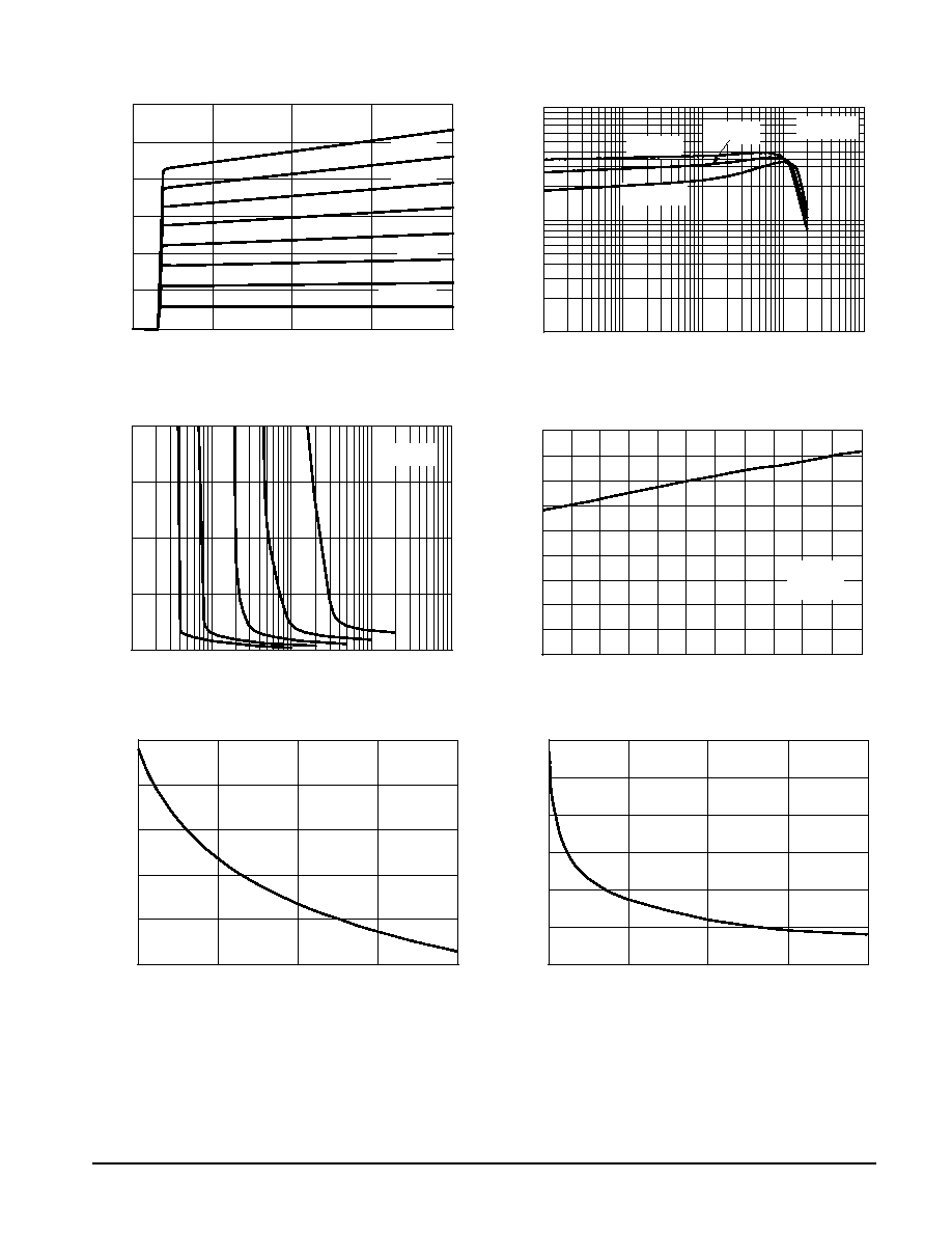
TYPICAL ELECTRICAL CHARACTERISTICS
Figure 1. IC VCE
VCE, COLLECTOR VOLTAGE (V)
Figure 2. DC Current Gain
IC, COLLECTOR CURRENT (mA)
Figure 3. Collector Saturation Region
IB, BASE CURRENT (mA)
Figure 4. On Voltage
IC, COLLECTOR CURRENT (mA)
I C
, COLLECT
OR
CURRENT
(mA)
60
0
50
40
30
20
10
0
2
4
6
8
TA = 25
°
C
160
µ
A
140
µ
A
120
µ
A
100
µ
A
80
µ
A
60
µ
A
40
µ
A
IB = 20
µ
A
DC CURRENT
GAIN
1000
0.1
100
10
1
10
100
TA = 25
°
C
TA = 25
°
C
TA = 75
°
C
VCE = 10 V
V
CE
, COLLECT
OR-EMITTER
VOL
T
AGE (V)
2
0.01
1.5
1
0.5
0
0.1
1
10
100
TA = 25
°
C
COLLECT
OR VOL
T
AGE
(mV)
900
0.2
800
700
600
500
400
300
200
100
0.5
1
5
10
20
40
60
80
100
150
200
TA = 25
°
C
VCE = 5 V
0
Figure 5. Capacitance
VCB (V)
Figure 6. Capacitance
VEB (V)
20
0
18
16
14
12
10
1
2
3
4
7
0
C
ib
, INPUT
CAP
ACIT
ANCE
(pF)
6
5
4
3
2
1
10
20
30
40
C
ob
, CAP
ACIT
ANCE
(pF)
2SC4617
3
Motorola SmallSignal Transistors, FETs and Diodes Device Data
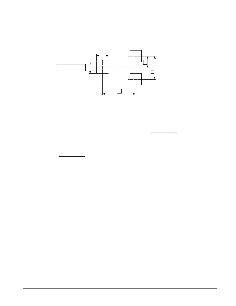
MINIMUM RECOMMENDED FOOTPRINT FOR SURFACE MOUNTED APPLICATIONS
Surface mount board layout is a critical portion of the total
design. The footprint for the semiconductor packages must
be the correct size to insure proper solder connection
interface between the board and the package. With the
correct pad geometry, the packages will self align when
subjected to a solder reflow process.
ÉÉÉ
ÉÉÉ
ÉÉÉ
ÉÉÉ
ÉÉÉ
ÉÉÉ
ÉÉÉ
ÉÉÉ
ÉÉÉ
1.4
1
0.5 min. (3x)
0.5 min. (3x)
TYPICAL
0.5
SOLDERING PATTERN
Unit: mm
SOT416/SC90 POWER DISSIPATION
The power dissipation of the SOT416/SC90 is a function
of the pad size. This can vary from the minimum pad size for
soldering to the pad size given for maximum power
dissipation. Power dissipation for a surface mount device is
determined by TJ(max), the maximum rated junction tempera-
ture of the die, R
JA, the thermal resistance from the device
junction to ambient; and the operating temperature, TA.
Using the values provided on the data sheet, PD can be
calculated as follows.
PD =
TJ(max) TA
R
JA
The values for the equation are found in the maximum
ratings table on the data sheet. Substituting these values into
the equation for an ambient temperature TA of 25
°
C, one can
calculate the power dissipation of the device which in this
case is 125 milliwatts.
PD =
150
°
C 25
°
C
1000
°
C/W
= 125 milliwatts
The 1000
°
C/W assumes the use of the recommended
footprint on a glass epoxy printed circuit board to achieve a
power dissipation of 125 milliwatts. Another alternative would
be to use a ceramic substrate or an aluminum core board
such as Thermal Clad
TM
. Using a board material such as
Thermal Clad, a higher power dissipation can be achieved
using the same footprint.
SOLDERING PRECAUTIONS
The melting temperature of solder is higher than the rated
temperature of the device. When the entire device is heated
to a high temperature, failure to complete soldering within a
short time could result in device failure. Therefore, the
following items should always be observed in order to
minimize the thermal stress to which the devices are
subjected.
·
Always preheat the device.
·
The delta temperature between the preheat and
soldering should be 100
°
C or less.*
·
When preheating and soldering, the temperature of the
leads and the case must not exceed the maximum
temperature ratings as shown on the data sheet. When
using infrared heating with the reflow soldering method,
the difference should be a maximum of 10
°
C.
·
The soldering temperature and time should not exceed
260
°
C for more than 10 seconds.
·
When shifting from preheating to soldering, the
maximum temperature gradient should be 5
°
C or less.
·
After soldering has been completed, the device should
be allowed to cool naturally for at least three minutes.
Gradual cooling should be used as the use of forced
cooling will increase the temperature gradient and result
in latent failure due to mechanical stress.
·
Mechanical stress or shock should not be applied during
cooling
* Soldering a device without preheating can cause excessive
thermal shock and stress which can result in damage to the
device.
2SC4617
4
Motorola SmallSignal Transistors, FETs and Diodes Device Data
SOLDER STENCIL GUIDELINES
Prior to placing surface mount components onto a printed
circuit board, solder paste must be applied to the pads. A
solder stencil is required to screen the optimum amount of
solder paste onto the footprint. The stencil is made of brass
or stainless steel with a typical thickness of 0.008 inches.
The stencil opening size for the surface mounted package
should be the same as the pad size on the printed circuit
board, i.e., a 1:1 registration.
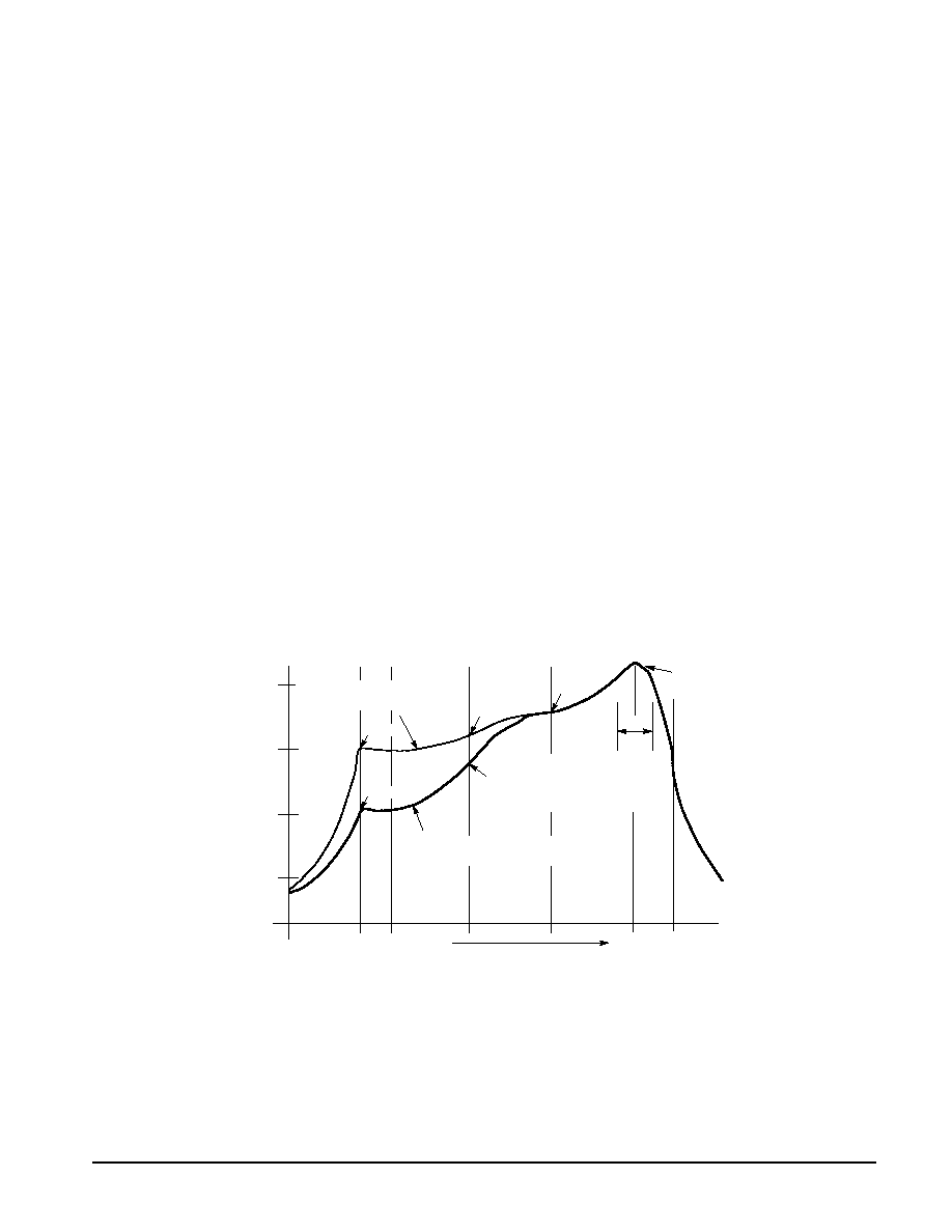
TYPICAL SOLDER HEATING PROFILE
For any given circuit board, there will be a group of control
settings that will give the desired heat pattern. The operator
must set temperatures for several heating zones, and a
figure for belt speed. Taken together, these control settings
make up a heating "profile" for that particular circuit board.
On machines controlled by a computer, the computer
remembers these profiles from one operating session to the
next. Figure 7 shows a typical heating profile for use when
soldering a surface mount device to a printed circuit board.
This profile will vary among soldering systems but it is a good
starting point. Factors that can affect the profile include the
type of soldering system in use, density and types of
components on the board, type of solder used, and the type
of board or substrate material being used. This profile shows
temperature versus time. The line on the graph shows the
actual temperature that might be experienced on the surface
of a test board at or near a central solder joint. The two
profiles are based on a high density and a low density board.
The Vitronics SMD310 convection/infrared reflow soldering
system was used to generate this profile. The type of solder
used was 62/36/2 Tin Lead Silver with a melting point
between 177 189
°
C. When this type of furnace is used for
solder reflow work, the circuit boards and solder joints tend to
heat first. The components on the board are then heated by
conduction. The circuit board, because it has a large surface
area, absorbs the thermal energy more efficiently, then
distributes this energy to the components. Because of this
effect, the main body of a component may be up to 30
degrees cooler than the adjacent solder joints.
STEP 1
PREHEAT
ZONE 1
"RAMP"
STEP 2
VENT
"SOAK"
STEP 3
HEATING
ZONES 2 & 5
"RAMP"
STEP 4
HEATING
ZONES 3 & 6
"SOAK"
STEP 5
HEATING
ZONES 4 & 7
"SPIKE"
STEP 6
VENT
STEP 7
COOLING
200
°
C
150
°
C
100
°
C
50
°
C
TIME (3 TO 7 MINUTES TOTAL)
TMAX
SOLDER IS LIQUID FOR
40 TO 80 SECONDS
(DEPENDING ON
MASS OF ASSEMBLY)
205
°
TO 219
°
C
PEAK AT
SOLDER JOINT
DESIRED CURVE FOR LOW
MASS ASSEMBLIES
100
°
C
150
°
C
160
°
C
140
°
C
Figure 7. Typical Solder Heating Profile
DESIRED CURVE FOR HIGH
MASS ASSEMBLIES
170
°
C
2SC4617
5
Motorola SmallSignal Transistors, FETs and Diodes Device Data
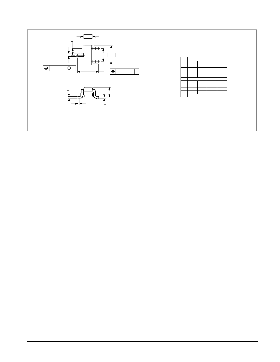
PACKAGE DIMENSIONS
CASE 46301
ISSUE A
SOT416/SC90
DIM
MIN
MAX
MIN
MAX
INCHES
MILLIMETERS
A
0.70
0.80
0.028
0.031
B
1.40
1.80
0.055
0.071
C
0.60
0.90
0.024
0.035
D
0.15
0.30
0.006
0.012
G
1.00 BSC
0.039 BSC
H
0.10
0.004
J
0.10
0.25
0.004
0.010
K
1.45
1.75
0.057
0.069
L
0.10
0.20
0.004
0.008
S
0.50 BSC
0.020 BSC
NOTES:
1. DIMENSIONING AND TOLERANCING PER ANSI
Y14.5M, 1982.
2. CONTROLLING DIMENSION: MILLIMETER.
M
0.20 (0.008)
B
A
B
S
D
G
3 PL
0.20 (0.008) A
K
J
L
C
H
3
2
1
STYLE 1:
PIN 1. BASE
2. EMITTER
3. COLLECTOR