
MOSEL VITELIC
1
V436616Y04VTG-10PC
3.3 VOLT 16M x 64 HIGH PERFORMANCE
100 MHZ SDRAM UNBUFFERED SODIMM
PRELIMINARY
V436616Y04VTG-10PC Rev. 0.8 October 2000
Features
s
JEDEC-standard 144 pin, Small-Outline, Dual in
line Memory Module (SODIMM)
s
Serial Presence Detect with E
2
PROM
s
Nonbuffered
s
Fully Synchronous, All Signals Registered on
Positive Edge of System Clock
s
Single +3.3V (� 0.3V) Power Supply
s
All Device Pins are LVTTL Compatible
s
8192 Refresh Cycles every 64 ms
s
Self-Refresh Mode
s
Internal Pipelined Operation; Column Address
can be changed every System Clock
s
Auto Precharge and Piecharge all Banks by A10
s
Data Mask Function by DQM
s
Mode Register Set Programming
s
Programmable (CAS Latency: 2, 3 Clocks)
Description
The V436616Y04VTG-10PC memory module is
organized 16,777,216 x 64 bits in a 144 pin
SODIMM. The 16M x 64 memory module uses 4
Mosel-Vitelic 16M x 16 SDRAM. The x64 modules
are ideal for use in high performance computer
systems where increased memory density and fast
access times are required.
Part Number
Speed
Grade
Configuration
V436616Y04VTG-10PC
-10PC
(100 MHz)
16M x 64
1
Pin 2 on Backside
Pin 144 on Backside
59
61
143
16M x 16
16M x 16
16M x 16
16M x 16

2
V436616Y04VTG-10PC Rev. 0.8 October 2000
MOSEL VITELIC
V436616Y04VTG-10PC
Pin Configurations (Front Side/Back Side)
Note:
1. RAS, CAS, WE CASx, CSx are active low signals.
Pin
Front
Pin
Front
Pin
Front
Pin
Back
Pin
Back
Pin
Back
1
2
3
4
5
6
7
8
9
10
11
12
13
14
15
16
17
18
19
20
21
22
23
24
VSS
VSS
DQ0
DQ32
DQ1
DQ33
DQ2
DQ34
DQ3
DQ35
VDD
VDD
DQ4
DQ36
DQ5
DQ37
DQ6
DQ38
DQ7
DQ39
VSS
VSS
DQMB0
DQMB4
25
26
27
28
29
30
31
32
33
34
35
36
37
38
39
40
41
42
43
44
45
46
47
48
DQMB1
DQMB5
VDD
VDD
A0
A3
A1
A4
A2
A5
VSS
VSS
DQ8
DQ40
DQ9
DQ41
DQ10
DQ42
DQ11
DQ43
VDD
VDD
DQ12
DQ44
49
50
51
52
53
54
55
56
57
58
59
60
61
62
63
64
65
66
67
68
69
70
71
72
DQ13
DQ45
DQ14
DQ46
DQ15
DQ47
VSS
VSS
NC
NC
NC
NC
CLK0
CKE0
VDD
VDD
RAS
CAS
WE
CKE1
CS0
NC
CS1
A12
73
74
75
76
77
78
79
80
81
82
83
84
85
86
87
88
89
90
91
92
93
94
95
96
NC
CLK1
VSS
VSS
NC
NC
NC
NC
VDD
VDD
DQ16
DQ48
DQ17
DQ49
DQ18
DQ50
DQ19
DQ51
VSS
VSS
DQ20
DQ52
DQ21
DQ53
97
98
99
100
101
102
103
104
105
106
107
108
109
110
111
112
113
114
115
116
117
118
119
120
DQ22
DQ54
DQ23
DQ55
VDD
VDD
A6
A7
A8
BA0
VSS
VSS
A9
BA1
A10
A11
VDD
VDD
DQMB2
DQMB6
DQMB3
DQMB7
VSS
VSS
121
122
123
124
125
126
127
128
129
130
131
132
133
134
135
136
137
138
139
140
141
142
143
144
DQ24
DQ56
DQ25
DQ57
DQ26
DQ58
DQ27
DQ59
VDD
VDD
DQ28
DQ60
DQ29
DQ61
DQ30
DQ62
DQ31
DQ63
VSS
VSS
SDA
SCL
VDD
VDD
Pin Names
A0�A12, BA0, BA1
Address, Bank Select
DQ0�DQ63
Data Inputs/Outputs
RAS
Row Address Strobes
CAS
Column Address Strobes
WE
Write Enable
CS0, CS1
Chip Select
DQMB0�DQMB7
Output Enable
CKE0, CKE1
Clock Enable
CLK0, CLK1
Clock
SDA
Serial Input/Output
SCL
Serial Clock
VDD
Power Supply
VSS
Ground
NC
No Connect (Open)
MOSEL VITELIC
V436616Y04VTG-10PC
3
V436616Y04VTG-10PC Rev. 0.8 October 2000
Part Number Information
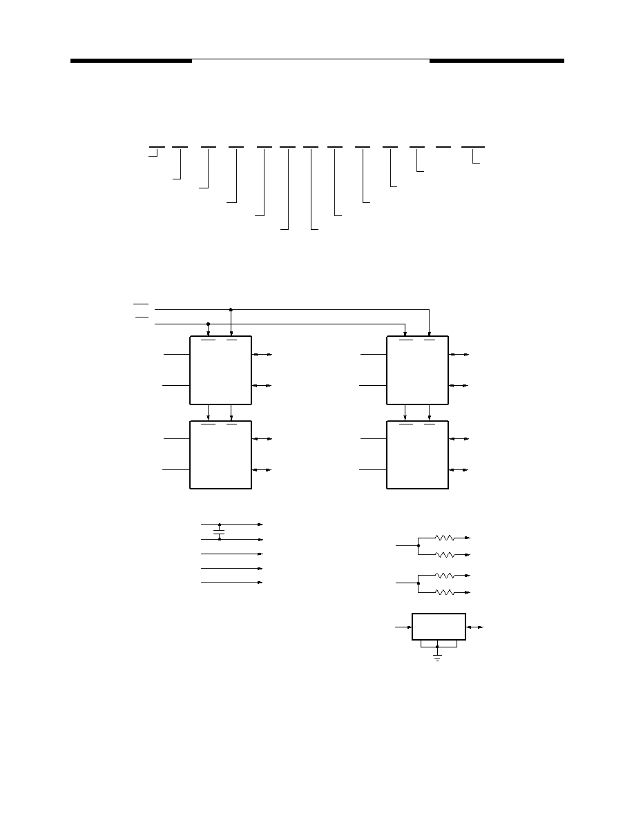
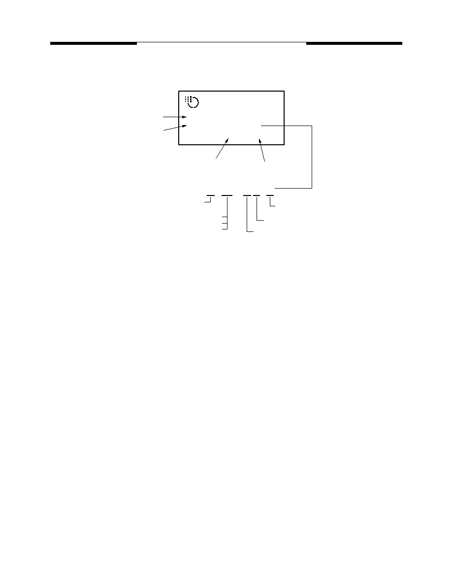
Block Diagram
SDRAM
3.3V
4
MOSEL-VITELIC
MANUFACTURED
V
144 PIN UNBUFFERED
SODIMM x16 COMPONENT
Y
REFRESH
RATE 8K
0
3
DEPTH
16
4 BANKS
4
TSOP
WIDTH
66
LVTTL
V
GOLD
G
10PC
-
-10PC PC100 2-2-2
T
WE
CSO
U0�U7
A0�A12, BA0, BA1
VDD
U0�U3
CKE0
U4�U7
CKEI
U0�U7
U0, U1
CLK0
VSS
U2, U3
10
SCL
SDA
10
U4, U5
CLKI
U6, U7
10
10
SPD
A0
A1
A2
DQMB4
DQMB5
DQ32�39
DQ40�47
UDQM
U2
LDQM
DQMB0
DQMB1
DQ0�7
DQ8�15
UDQM
U0
LDQM
DQMB6
DQMB7
DQ43�54
DQ55�63
UDQM
U3
LDQM
DQMB2
DQMB3
DQ16�23
DQ24�31
UDQM
U1
LDQM
CS
WE
CS
WE
CS
WE
CS
WE
C1�C4
4
V436616Y04VTG-10PC Rev. 0.8 October 2000
MOSEL VITELIC
V436616Y04VTG-10PC
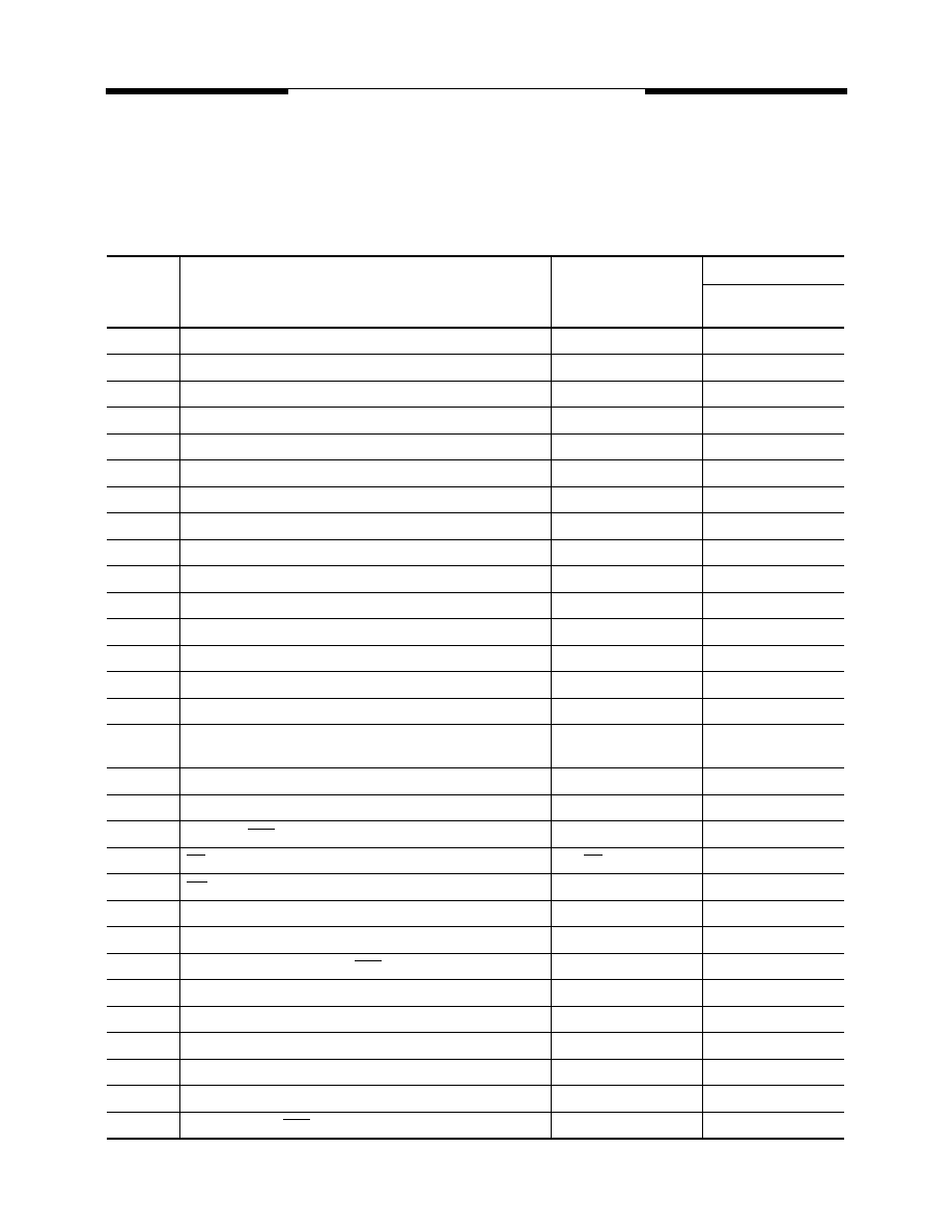
Serial Presence Detect Information
A serial presence detect storage device �
E
2
PROM � is assembled onto the module. Informa-
tion about the module configuration, speed, etc. is
written into the E
2
PROM device during module pro-
duction using a serial presence detect protocol (I
2
C
synchronous 2-wire bus)
SPD-Table for -10 PC modules:
Byte
Number
Function Described
SPD Entry Value
Hex Value
100 MHz
-10PC
0
Number of SPD bytes
128
80
1
Total bytes in Serial PD
256
08
2
Memory Type
SDRAM
04
3
Number of Row Addresses (without BS bits)
13
0D
4
Number of Column Addresses (for x16 SDRAM)
9
09
5
Number of DIMM Banks
1
01
6
Module Data Width
64
40
7
Module Data Width (continued)
0
00
8
Module Interface Levels
LVTTL
01
9
SDRAM Cycle Time at CL=3
10.0 ns
A0
10
SDRAM Access Time from Clock at CL=3
6.0 ns
60
11
Dimm Config (Error Det/Corr.)
none
00
12
Refresh Rate/Type
Self-Refresh, 15.6
�
s
80
13
SDRAM width, Primary
x16
10
14
Error Checking SDRAM Data Width
n/a / x8
00
15
Minimum Clock Delay from Back to Back
Random Column Address
t
ccd
= 1 CLK
01
16
Burst Length Supported
1, 2, 4, 8, full page
8F
17
Number of SDRAM Banks
4
04
18
Supported CAS Latencies
CL = 2 & 3
06
19
CS Latencies
CS Latency = 0
01
20
WE Latencies
WL = 0
01
21
SDRAM DIMM Module Attributes
Non Buffered/Non Reg.
00
22
SDRAM Device Attributes: General
Vcc tol � 10%
0E
23
Minimum Clock Cycle Time at CAS Latency = 2
10.0 ns
A0
24
Maximum Data Access Time from Clock for CL = 2
6.0 ns
60
25
Minimum Clock Cycle Time at CL = 1
Not Supported
00
26
Maximum Data Access Time from Clock at CL = 1
Not Supported
00
27
Minimum Row Precharge Time t
RP
20 ns
14
28
Minimum Row Active to Row Active Delay t
RRD
16 ns
10
29
Minimum RAS to CAS Delay t
RCD
20 ns
14

MOSEL VITELIC
V436616Y04VTG-10PC
5
V436616Y04VTG-10PC Rev. 0.8 October 2000
Absolute Maximum Ratings
DC Characteristics
T
A
= 0
�
C to 70
�
C; V
SS
= 0 V; V
DD
, V
DDQ
= 3.3V
�
0.3V
30
Minimum RAS Pulse Width t
RAS
48 ns
30
31
Module Bank Density (Per Bank)
128 MByte
20
32
SDRAM Input Setup Time
2.0 ns
20
33
SDRAM Input Hold Time
1 ns
10
34
SDRAM Data Input Setup Time
2.0 ns
20
35
SDRAM Data Input Hold Time
1 ns
10
36-61
Superset Information (May be used in Future)
00
62
SPD Revision
Revision 1.2
12
63
Checksum for Bytes 0 - 62
18
64-125
Manufacturers's Information (Optional)
00
126
Max. Frequency Specification
100 MHz
64
127
100 MHz Support Details
00
128+
Unused Storage Location
00
Parameter
Max.
Units
Voltage on VDD Supply Relative to V
SS
-1 to 4.6
V
Voltage on Input Relative to V
SS
-1 to 4.6
V
Operating Temperature
0 to +70
�C
Storage Temperature
-55 to 125
�C
Power Dissipation
4
W
Symbol
Parameter
Limit Values
Unit
Min.
Max.
V
IH
Input High Voltage
2.0
V
CC
+0.3
V
V
IL
Input Low Voltage
�0.3
0.8
V
V
OH
Output High Voltage (I
OUT
= �4.0 mA)
2.4
--
V
V
OL
Output Low Voltage (I
OUT
= 4.0 mA)
--
0.4
V
I
I(L)
Input Leakage Current, any input
(0 V < V
IN
< 3.6 V, all other inputs = 0V)
�20
20
�
A
I
O(L)
Output leakage current
(DQ is disabled, 0V < V
OUT
< V
CC
)
�20
20
�
A
SPD-Table for -10 PC modules: (Continued)
Byte
Number
Function Described
SPD Entry Value
Hex Value
100 MHz
-10PC
6
V436616Y04VTG-10PC Rev. 0.8 October 2000
MOSEL VITELIC
V436616Y04VTG-10PC
Capacitance
T
A
= 0
�
C to 70
�
C; V
DD
= 3.3V
�
0.3V, f = 1 MHz
Standby and Refresh Currents
1
T
A
= 0
�
C to 70
�
C, V
CC
= 3.3V
�
0.3V
Symbol
Parameter
Limit Values (Max.)
Unit
C
I1
Input Capacitance (A0 to A11, RAS, CAS, WE)
40
pF
C
I2
Input Capacitance (CS0, CSI)
25
pF
C
ICL
Input Capacitance (CLK0-CLK1)
28
pF
C
I3
Input Capacitance (CKE0, CKEI)
20
pF
C
I4
Input Capacitance (DQMB0-DQMB7)
10
pF
C
SC
Input Capacitance (SCL, SA0-2)
8
pF
C
IO
Input/Output Capacitance
18
pF
Symbol Parameter
Test Conditions
16M x 64
Unit
Note
I
CC
1
Operating Current
Burst length = 4, CL = 3
t
RC
> = t
RC
(min),
t
CK
> = t
CK
(min), IO = 0 mA
2 Bank Interleave Operation
680
mA
1,2
I
CC
2P
Precharged Standby Current in Power
Down Mode
CKE< = V
IL
(max), t
CK
> = t
CK
(min)
8
mA
I
CC
2N
Precharged Standby Current in
Non-Power Down Mode
CKE> = V
IH
(min), t
CK
> = t
CK
(min), Input
changed once in 3 cycles
120
mA
CS = High
I
CC
3P
Active Standby Current in Power
Down Mode
CKE< = V
IL
(max), t
CK
> = t
CK
(min)
40
mA
I
CC
3N
Active Standby Current in Non-Power
Down Mode
CKE> = V
IH
(min), t
CK
> = t
CK
(min), Input
changed one time
180
mA
CS = High
I
CC
4
Burst Operating Current
Burst length = Full Page,
t
RC
= Infinite, CL = 3,
t
CK
> = t
CK
(min), IO = 0 mA
2 Banks Activated
480
mA
1, 2
I
CC
5
Auto Refresh Current
t
RC
>= t
RC
(min)
880
mA
1,2
I
CC
6
Self Refresh Current
CKE = <0,2 V
Standard
12
mA
1,2
L-Version
6

MOSEL VITELIC
V436616Y04VTG-10PC
7
V436616Y04VTG-10PC Rev. 0.8 October 2000
AC Characteristics
3,4
T
A
= 0� to 70
�
C; V
SS
= 0V; V
CC
= 3.3V
�
0.3V, t
T
= 1 ns
#
Symbol
Parameter
Limit Values
Unit
Note
-10PC
Min.
Max.
Clock and Clock Enable
1
t
CK
Clock Cycle Time
CAS Latency = 3
CAS Latency = 2
10
10
ns
ns
2
f
CK
System frequency
CAS Latency = 3
CAS Latency = 2
�
�
100
100
MHz
MHz
3
t
AC
Clock Access Time
CAS Latency = 3
CAS Latency = 2
�
�
6
6
ns
ns
4,5
4
t
CH
Clock High Pulse Width
3
�
ns
6
5
t
CL
Clock Low Pulse Width
3
�
ns
6
6
t
CS
Input Setup time
2
�
ns
7
7
t
CH
Input Hold Time
1
�
ns
7
8
t
CKSP
CKE Setup Time (Power down mode)
2
�
ns
8
9
t
CKSR
CKE Setup Time (Self Refresh Exit)
8
�
ns
9
10
t
T
Transition time (rise and fall)
1
�
ns
Common Parameters
11
t
RCD
RAS to CAS delay
20
�
ns
12
t
RC
Cycle Time
70
120k
ns
13
t
RAS
Active Command Period
45
�
ns
14
t
RP
Precharge Time
20
�
ns
15
t
RRD
Bank to Bank Delay Time
16
�
ns
16
t
CCD
CAS to CAS delay time
(same bank)
1
�
CLK
Refresh Cycle
17
t
SREX
Self Refresh Exit Time
10
�
ns
9
18
t
REF
Refresh Period (8192 cycles)
64
�
ms
8
Read Cycle
19
t
OH
Data Out Hold Time
3
�
ns
4
20
t
LZ
Data Out to Low Impedance Time
0
�
ns
21
t
HZ
Data Out to High Impedance Time
3
9
ns
10
22
t
DQZ
DQM Data Out Disable Latency
2
�
CLK
Write Cycle
23
t
DPL
Data input to Precharge (write recovery)
1
�
CLK
24
t
DAL
Data In to Active/refresh
5
�
CLK
11
25
t
DQW
DQM Write Mask Latency
0
�
CLK

8
V436616Y04VTG-10PC Rev. 0.8 October 2000
MOSEL VITELIC
V436616Y04VTG-10PC
Notes:
1.
The specified values are valid when addresses are changed no more than once during t
CK
(min.) and when No
Operation commands are registered on every rising clock edge during t
RC
(min). Values are shown per module
bank.
2.
The specified values are valid when data inputs (DQ's) are stable during t
RC
(min.).
3.
All AC characteristics are shown for device level.
An initial pause of 100
�
s is required after power-up, then a Precharge All Banks command must be given followed
by 8 Auto Refresh (CBR) cycles before the Mode Register Set Operation can begin.
4.
AC timing tests have V
IL
= 0.4V and V
IH
= 2.4V with the timing referenced to the 1.4V crossover point. The transition
time is measured between V
IH
and V
IL
. All AC measurements assume t
T
= 1 ns with the AC output load circuit
shown. Specific tac and toh parameters are measured with a 50 pF only, without any resistive termination and with
a input signal of 1V / ns edge rate between 0.8V and 2.0V.
5.
If clock rising time is longer than 1 ns, a time (t
T
/2 -0.5) ns has to be added to this parameter.
6.
Rated at 1.5V
7.
If t
T
is longer than 1 ns, a time (t
T
-1) ns has to be added to this parameter.
8.
Any time that the refresh Period has been exceeded, a minimum of two Auto (CBR) Refresh commands must be
given to "wake-up" the device.
9.
Self Refresh Exit is a synchronous operation and begins on the 2nd positive clock edge after CKE returns high.
Self Refresh Exit is not complete until a time period equal to t
RC
is satisfied once the Self Refresh Exit command
is registered.
10.
Referenced to the time which the output achieves the open circuit condition, not to output voltage levels.
11.
t
DAL
is equivalent to t
DPL
+ t
RP
.
1.4V
1.4V
tSETUP
tHOLD
tAC
tAC
tLZ
tOH
tHZ
CLOCK
INPUT
OUTPUT
50 pF
I/O
Z=50 Ohm
+ 1.4 V
50 Ohm
2.4V
0.4V
t
T
tCL
tCH
I/O
Measurement conditions for
tac and toh
50 pF
MOSEL VITELIC
V436616Y04VTG-10PC
9
V436616Y04VTG-10PC Rev. 0.8 October 2000
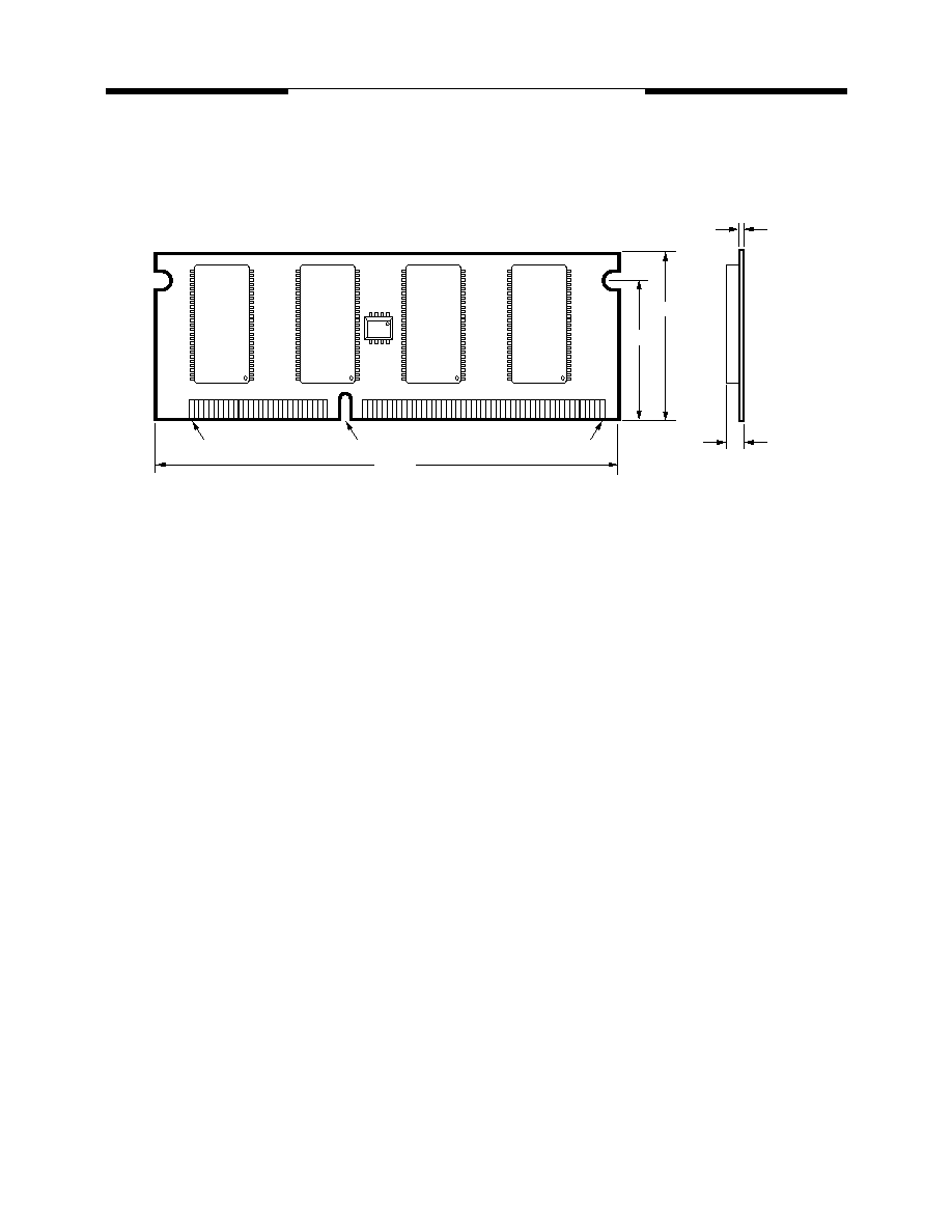
Package Diagram
144 Pin SODIMM
2.661
1.25
0.039
0.090
0.787
1
Pin 2 on Backside
3.3V
Pin 144 on Backside
28
29
143
NOTE:
1. All dimensions in inches.
Tolerances
�
0.005 unless otherwise specified.
10
V436616Y04VTG-10PC Rev. 0.8 October 2000
MOSEL VITELIC
V436616Y04VTG-10PC
Module Label Information
C
L
= 2 (CLK)
t
RCD
= 2 (CLK)
t
RP
= 2 (CLK)
t
AC
= 6 ns
222
U
UNBUFFERED DIMM
PC100
6
Intel SPD Revision 1.2
12
V436616Y04VTG-10PC
PC100U-222-612-A
Taiwan XXXX-XXXXXXX
A
Gerber file Intel
�
PC100 x 8 Based
-
-
-
MOSEL VITELIC
Part Number
DIMM manufacture date code
Trace Code
Criteria of PC100 or PC133
(refer to MVI datasheet)

MOSEL VITELIC
WORLDWIDE OFFICES
V436616Y04VTG-10PC
� Copyright 2000, MOSEL VITELIC Inc.
10/00
Printed in U.S.A.
MOSEL VITELIC
3910 N. First Street, San Jose, CA 95134-1501 Ph: (408) 433-6000 Fax: (408) 433-0952 Tlx: 371-9461
The information in this document is subject to change without
notice.
MOSEL VITELIC makes no commitment to update or keep cur-
rent the information contained in this document. No part of this
document may be copied or reproduced in any form or by any
means without the prior written consent of MOSEL-VITELIC.
MOSEL VITELIC subjects its products to normal quality control
sampling techniques which are intended to provide an assurance
of high quality products suitable for usual commercial applica-
tions. MOSEL VITELIC does not do testing appropriate to provide
100% product quality assurance and does not assume any liabil-
ity for consequential or incidental arising from any use of its prod-
ucts. If such products are to be used in applications in which
personal injury might occur from failure, purchaser must do its
own quality assurance testing appropriate to such applications.
U.S. SALES OFFICES
U.S.A.
3910 NORTH FIRST STREET
SAN JOSE, CA 95134
PHONE: 408-433-6000
FAX: 408-433-0952
HONG KONG
19 DAI FU STREET
TAIPO INDUSTRIAL ESTATE
TAIPO, NT, HONG KONG
PHONE: 852-2666-3307
FAX: 852-2664-2406
TAIWAN
7F, NO. 102
MIN-CHUAN E. ROAD, SEC. 3
TAIPEI
PHONE: 886-2-2545-1213
FAX: 886-2-2545-1209
NO 19 LI HSIN ROAD
SCIENCE BASED IND. PARK
HSIN CHU, TAIWAN, R.O.C.
PHONE: 886-3-579-5888
FAX: 886-3-566-5888
SINGAPORE
10 ANSON ROAD #23-13
INTERNATIONAL PLAZA
SINGAPORE 079903
PHONE: 65-3231801
FAX: 65-3237013
JAPAN
ONZE 1852 BUILDING 6F
2-14-6 SHINTOMI, CHUO-KU
TOKYO 104-0041
PHONE: 03-3537-1400
FAX: 03-3537-1402
UK & IRELAND
SUITE 50, GROVEWOOD
BUSINESS CENTRE
STRATHCLYDE BUSINESS
PARK
BELLSHILL, LANARKSHIRE,
SCOTLAND, ML4 3NQ
PHONE: 44-1698-748515
FAX: 44-1698-748516
GERMANY
(CONTINENTAL
EUROPE & ISRAEL)
BENZSTRASSE 32
71083 HERRENBERG
GERMANY
PHONE: +49 7032 2796-0
FAX: +49 7032 2796 22
NORTHWESTERN
3910 NORTH FIRST STREET
SAN JOSE, CA 95134
PHONE: 408-433-6000
FAX: 408-433-0952
SOUTHWESTERN
302 N. EL CAMINO REAL #200
SAN CLEMENTE, CA 92672
PHONE: 949-361-7873
FAX: 949-361-7807
CENTRAL,
NORTHEASTERN &
SOUTHEASTERN
604 FIELDWOOD CIRCLE
RICHARDSON, TX 75081
PHONE: 972-690-1402
FAX: 972-690-0341