/home/web/doc/html/mitsumi/182053
MITSUMI
Secondary Control for Energy-saving AC Adaptors MM1529
Secondary Control for Energy-saving AC Adaptors
Monolithic IC MM1529
Outline
This IC is a secondary control IC for AC adaptors with energy-saving mode, and switches to energy-saving
mode when there is no load current flowing to reduce AC adaptor power consumption. When normal mode
load current flows, it switches automatically to normal mode and supplies power in response to the load. To
control the primary oscillator, this IC controls two photocouplers for rated voltage rated current control and
switching between energy-saving and normal modes.
Features
(1) Automatic switching between energy-saving mode and normal mode
(2) Current consumption (energy-saving mode)
60µA
(3) Current consumption (normal mode)
1.7mA
(4) Reference voltage (internal/output inversion voltage)
1.250V±25mV
(5) Uses two photocouplers to control primary side oscillator.
(6) Photocouplers are for rated voltage rated current control and switching between energy-saving and
normal modes.
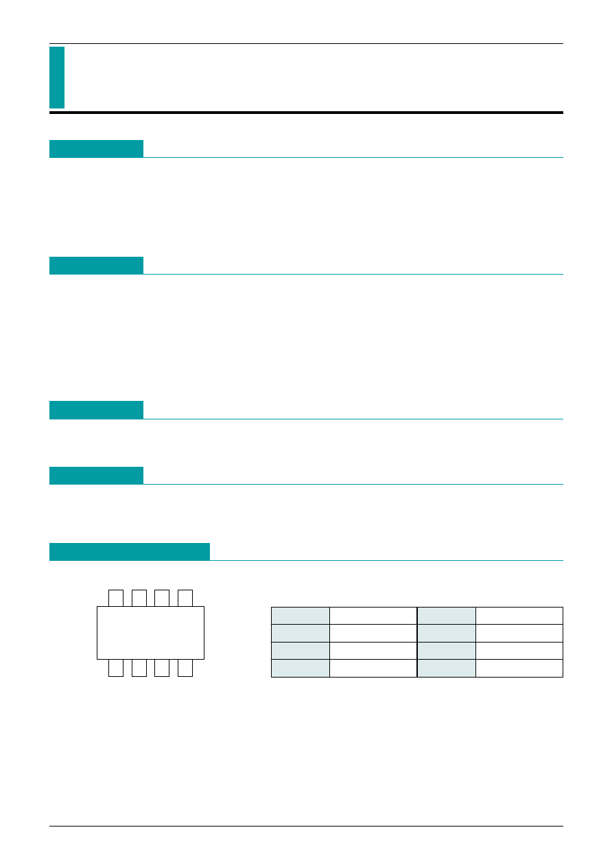
Package
SOP-8D
Applications
(1) AC adaptors (celler phones, movies, PDA, laptop PCs, others)
(2) Chargors (celler phones, movies, PDA, laptop PCs, others)
MITSUMI
Pin Connetion Diagram
1
4
3
2
8
5
6
7
SOP-8D
1
PO1
2
PO2
3
GND
4
CS
5
REF
6
OUT
7
CNT
8
V
CC
MITSUMI
Secondary Control for Energy-saving AC Adaptors MM1529
MITSUMI
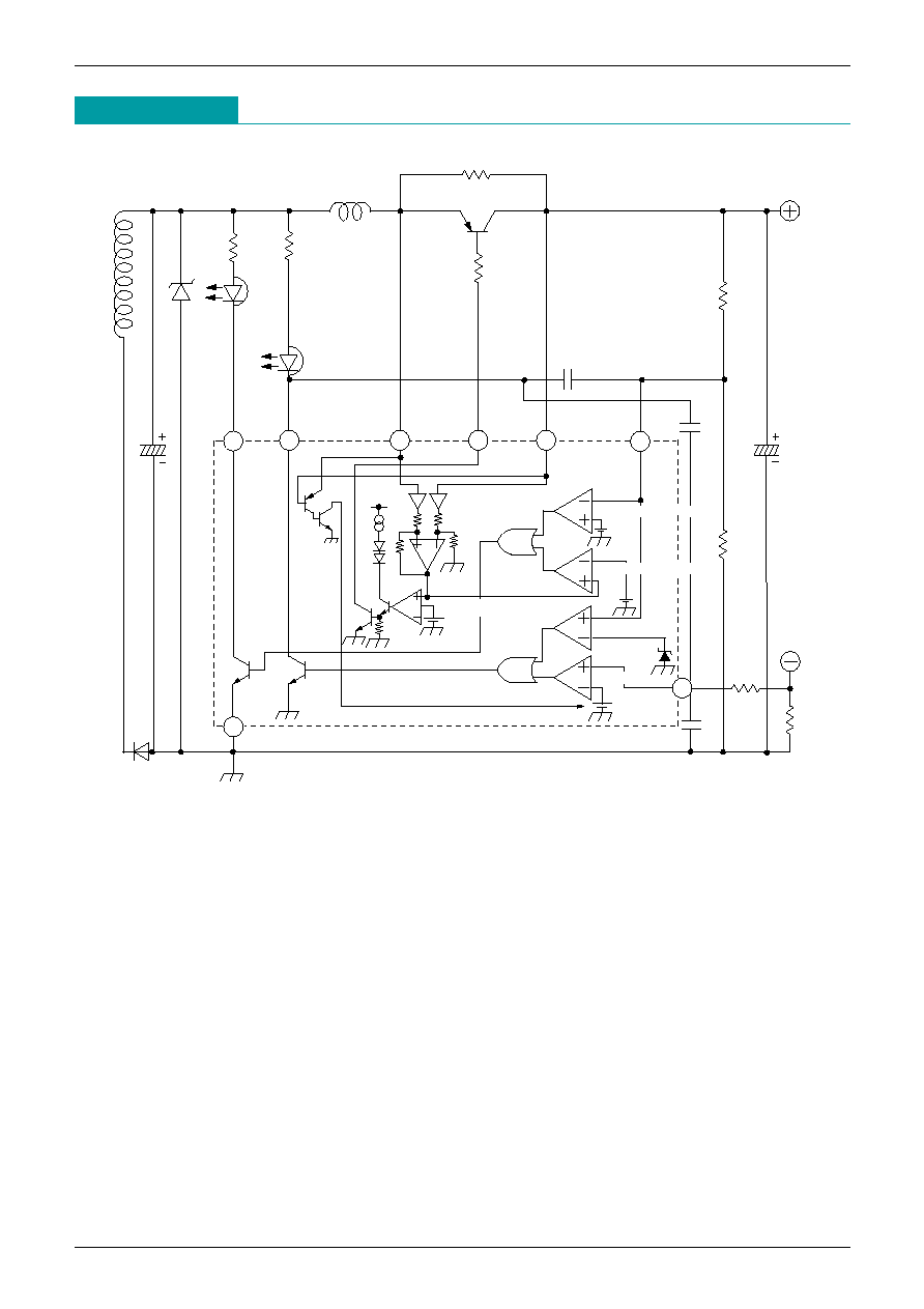
Block Diagram
8
1
2
3
4
5
6
7
R
L
1
R
L
2
PO2
PO1
V
CC
GND
R
L
B
R
L
S
ROS1
CS
C
OUT
RCS
V
CC
CNT
OUT
PC1
REF
L1
PC2
ROS2
Secondary transformer
Load detection resistor
For load detection
(1.0V)
Load connect detection
(0.2V)
REF control
(1.25V)
Rated current control
Reference voltage drop
Rated current detection resistor
Input/output error control
(0.2V)
For rated current
rated voltage
Voltage drop detection
(0.1144V)
MITSUMI
Secondary Control for Energy-saving AC Adaptors MM1529
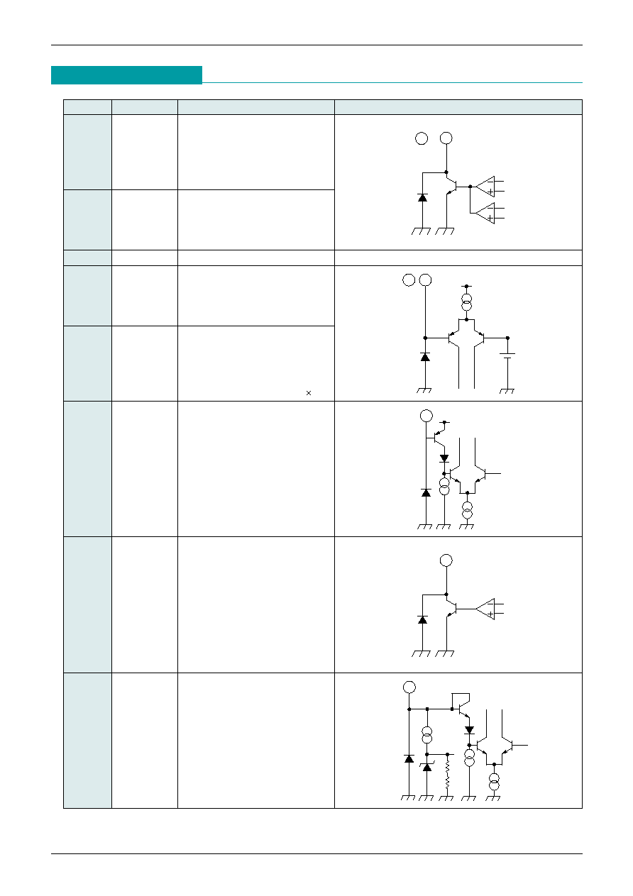
Terminal Explanation
Pin No.
Pin name
Function
Internal equivalent circuit
Rated current rated voltage
control photocoupler LED drive
1
PO1
pin.Connects cathode side of
diode.
Output load detection
2
PO2
photocoupler LED drive pin.
Connects cathode side of diode.
3
GND
Ground pin.
Overcurrent detection pin.
4
CS
Doubles as output- pin.
Connects overcurrent
resistor to GND pin.
Reference voltage input pin.
Connects R1 resistor to the OUT
5
REF
pin and R2 resistor to GND pin
to control output pin.
Output voltage={1+ (R
OS
1/ R
OS
2)} 1.25
Output +pin.
Connects load detection resistor
to Vcc pin and connects PNP
6
OUT
power transistor collector.
PNP power transistor control pin.
Connects to PNP power
transistor base.
7
CNT
+Power supply pin.
Doubles as load detection pin.
Connects load detection
resistor to OUT pin
8
V
CC
and connects PNP power
transistor emitter.
1
2
4
5
V
CC
6 V
CC
7
8
1.25V
MITSUMI
Secondary Control for Energy-saving AC Adaptors MM1529
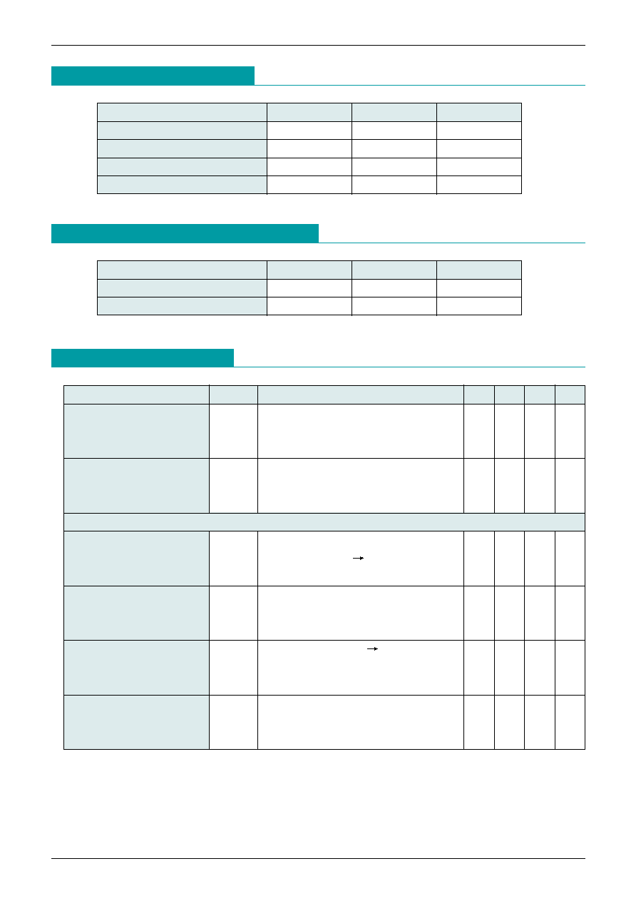
Electrical Characteristics
(V
CC
=5.0V , Ta=25°C Unless otherwise specified)
Item
Symbol
Test Conditions
Min. Typ. Max. Unit
V
OUT
=5.0V
Current consumption 1
I
CC1
V
REF
=1.2V
60
100
uA
(energy-saving mode)
V
CS
=0V
V
OUT
=4.7V
Current consumption 2
I
CC2
V
REF
=1.2V
1.7
3.5
mA
(normal mode)
V
CS
=0V
Voltage control
V
OUT
=5.0V R
L1
=500
Output inversion voltage
V
REFH
V
REF
:1.1V H R
L2
=1k
1.225 1.250 1.275
V
V
CS
=0V R
L3
=100
V
OUT
=5.0V
REF input current
I
REF
V
REF
=1.2V
15
100
nA
V
CS
=0V
V
CC
=4V 12V
Power supply voltage removal
PSRR1
V
REF
=V
REFH
60
70
dB
V
CS
=0V R
L1
=5k
V
OUT
=5.0V
P01 output inflow current
I
PO1-V
V
REF
=1.5V
5
17
mA
V
CS
=0V V
PO1
=0.5V
Absolute Maximum Ratings
(Ta=25°C)
Recommended Operating Conditions
Item
Symbol
Rating
Unit
Storage temperature
T
STG
-40~+125
°C
Operating temperature
T
OPR
-30~+85
°C
Supply voltage
V
CC
max.
-0.3~+18
V
Power dissipation
P
D
300 (Alone)
mW
Item
Symbol
Rating
Unit
Operating temperature
T
OPR
-30~+85
°C
Supply voltage
V
OP
+2.5~+12
V

MITSUMI
Secondary Control for Energy-saving AC Adaptors MM1529
MITSUMI
Item
Symbol Test
Conditions
Min. Typ. Max. Unit
Rated current control
V
OUT
=4.7V R
L1
=500
Output inversion voltage 1
V
CS1
V
REF
=1.2V R
L2
=1.2k
111.2 114.4 117.6
mV
(rated current control)
V
CS
: L H R
L3
=1.4k
V
CC
=2.0V
Output inversion voltage 2
V
CS2
V
OUT
=0V R
L1
=500
22
34
mV
(rated current control)
V
REF
=1.2V R
L2
=1.2k
V
CS
: L H R
L3
=1.4k
V
OUT
=5.0V
CS input current
I
CS
V
REF
=1.2V
15
100
nA
V
CS
=0.1V
V
CC
=4V 12V
Power supply voltage removal
PSRR2
V
REF
=1.2V
60
70
dB
V
CS
=V
CS1-
10mV R
L2
=5k
V
OUT
=4.7V
P01 output inflow current
I
PO1-I
V
REF
=1.2V
5
17
mA
V
CS
=0.2V V
PO1
=0.5V
Input/output error control
R
LS
=4.7k
Input/output error
V
LS
R
O
=5k
140
200
260
mV
control voltage
R
LB
=100
V
OUT
=4.7V
CNT output inflow current
I
CNT
V
REF
=1.2V
5
30
mA
V
CS
=0V V
CNT
=0.8V
V
OUT
=5.0V
OUT input current
I
OUT
V
REF
=1.2V
2
100
nA
V
CS
=0V
Load detection
V
OUT
=5.0V L R
L1
=500
Load detection voltage
V
LSP1
V
REF
=1.2V R
L2
=1k
170
200
230
mV
V
CS
=0V R
L3
=100
V
OUT
=L 5.0V R
L1
=500
Energy-saving detection voltage
V
LSP2
V
REF
=1.2V R
L2
=1k
97
115
133
mV
(load detection release voltage)
V
CS
=0V R
L3
=100
V
OUT
=5.0V R
L1
=500
Voltage drop detection
V
REFL
V
REF
=1.2V L R
L2
=1k
0.975 1.000 1.025
V
V
CS
=0V R
L3
=100
V
OUT
=4.7V
PO2 output inflow current
I
PO2
V
REF
=1.2V
5.0
9.0
mA
V
CS
=0V V
PO2
=0.5V