MITSUMI
RGB Video Amplifier with OSD Input MM1381, 1382, 1383
RGB Video Amplifier with OSD Input
Monolithic IC MM1381, 1382, 1383
Outline
MM1381XD, MM1382XD and MM1383XD are wideband RGB video amplifiers with OSD input, developed for
use in monitors. The main differences between them are video amp bandwidth and output rise time, and
output fall time.
Features
1. Built-in wideband video amp
110MHz
@ -3dB (4V
P-P
output)
2. OSD input has TTL interface
bandwidth 50MHz
3. Output voltage less than 0.1V for blanking
4. High-speed switching between VIDEO/OSD
5. Each channel has an independent drive pin for color balance adjustment
6. Built-in high impedance DC contrast control, 0~4V (> 40dB range)
7. Built-in high impedance DC drive control, 0~4V (±3dB range)
8. Built-in high impedance DC OSD contrast control, 0~4V (> 40dB range)
9. 7V
P-P
output swing (band slightly attenuated)
10Output can drive hybrid or discrete CRT drivers directly
Package
DIP-28C (MM1381XD, MM1382XD, MM1383XD)
Applications
1. High resolution RGB CRT monitors with OSD function
2. AGC amps for video
3. Gain and DC offset control
4. LCD or CCD system interface amp
Model
MM1381
MM1382
MM1383
Video amp band
85MHz
110MHz
140MHz
Output rise time
3.5nS
3.0nS
2.3nS
Output fall time
4.5nS
4.0nS
3.3nS
MM1382XD is described here as the representative model.
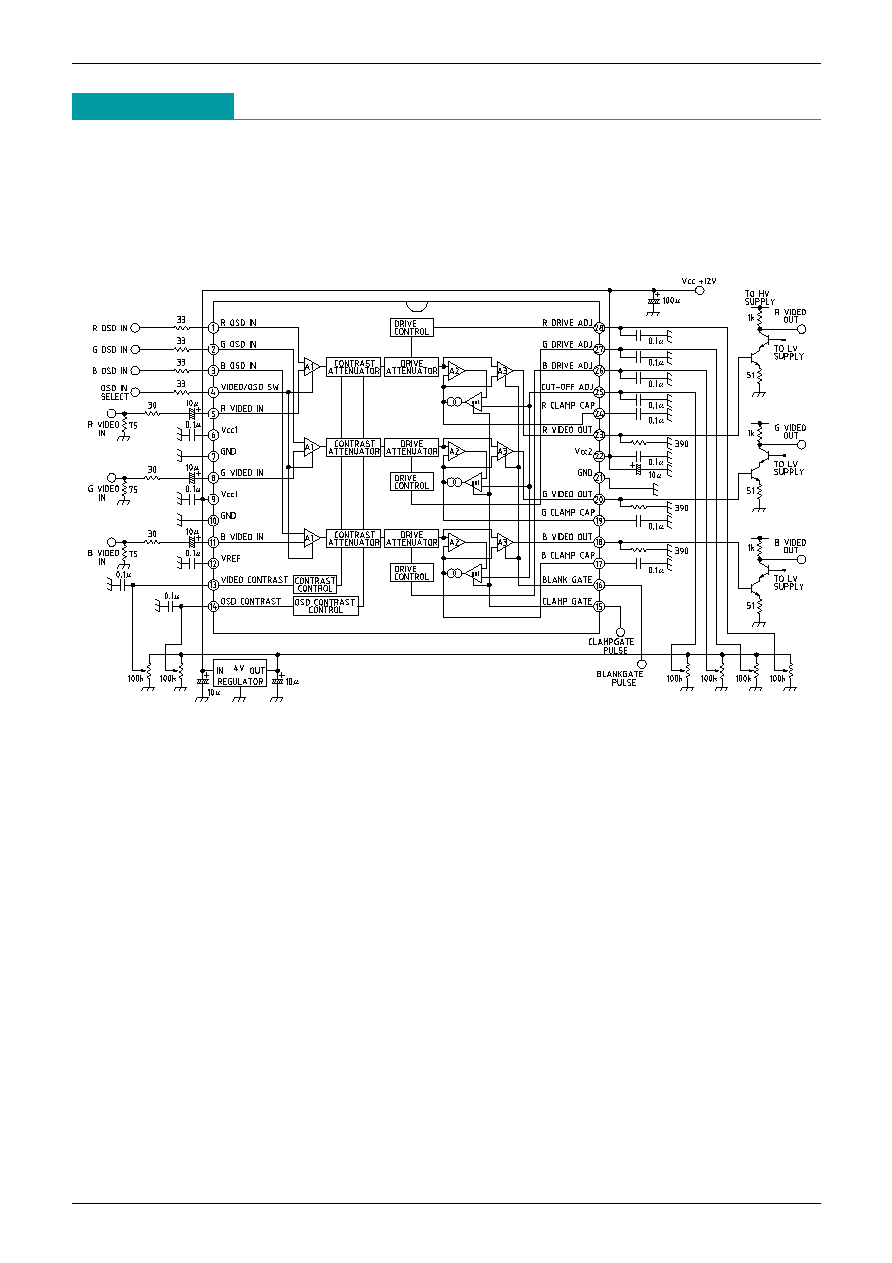
MM1382 is a wideband video amp system with OSD input, developed for use in high resolution RGB
monitors. MM1382 has three matched video amps with a blanking function. All DC control input is high
impedance, and the operating range is set for easy interface with serial bus control systems, at 0~4V. The
OSD section has three TTL inputs and DC contrast control. OSD signals have TTL input interface, and these
signals are made internally so that OSD input low level and video black level are the same. OSD display color
balance follows video signal color balance control adjustment. In addition, MM1382 has a built-in spot-killer
circuit that protects the CRT when monitor power is turned off.
MITSUMI
RGB Video Amplifier with OSD Input MM1381, 1382, 1383
Block Diagram
MITSUMI
RGB Video Amplifier with OSD Input MM1381, 1382, 1383
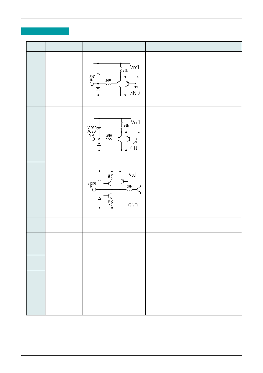
Pin Description
Pin no.
Pin name
Internal equivalent circuit diagram
Pin Description
1
R OSD IN
2
G OSD IN
3
B OSD IN
These inputs accept standard TTL input. Each
color is either completely ON (logic high) or
completely OFF (logic low). Connect unused
pins to ground with a 47k
resistor.
4
VIDEO/OSD
SWITCH
This input accepts standard TTL input.
H : OSD, L : VIDEO
Connect OSD to ground with a 47k
resistor
when not in use.
5
R VIDEO IN
8
G VIDEO IN
11
B VIDEO IN
Video inputs.
These inputs must be AC coupled using a
capacitor of at least 1µF. The ideal capacitance
is 10 (F. DC playback is done with these
inputs. Also, serial resistor of approximately
33
must be used.
6
V
CC
1
9
Power supply pin (except for output stage).
7
GND
10
21
GND pins.
The GND pins are all connected internally, and
must be connected on the board as well.
12
V
REF
Used for internal reference additional filter
capacitor. Voltage of this pin is 2.0V.
13
VIDEO CONTRAST
14
OSD CONTRAST
26
B DRIVE
27
G DRIVE
28
R DRIVE
Contrast control pin :
4V no attenuation
0V attenuation over 60dB
Drive control pin :
4V no attenuation
0V 12dB attenuation

MITSUMI
RGB Video Amplifier with OSD Input MM1381, 1382, 1383
Pin no.
Pin name
Internal equivalent circuit diagram
Pin Description
15
CLAMP GATE
16
BLANK GATE
These two pins accept TTL input and are active
low. Clamp gate supplies video signal DC
playback. Blank gate makes video output less
than 200mV.
17
B CLAMP CAP
19
G CLAMP CAP
24
R CLAMP CAP
External clamp capacitors are charged, then
discharged to the correction voltage required
for DC playback. Recommended value is
0.1µF.
18
B VIDEO OUT
20
G VIDEO OUT
23
R VIDEO OUT
Video output.
Output must have 390
impedance to obtain
the correct black level.
22
V
CC
2
Output stage power supply pin.
Internal connection to V
CC
1 does not exist.
25
RGB CUT OFF
ADJUST
Sets video output black level for all three
channels.
Range : 0~4V
Minimum value for black level is limited to
approximately 300mV.
MITSUMI
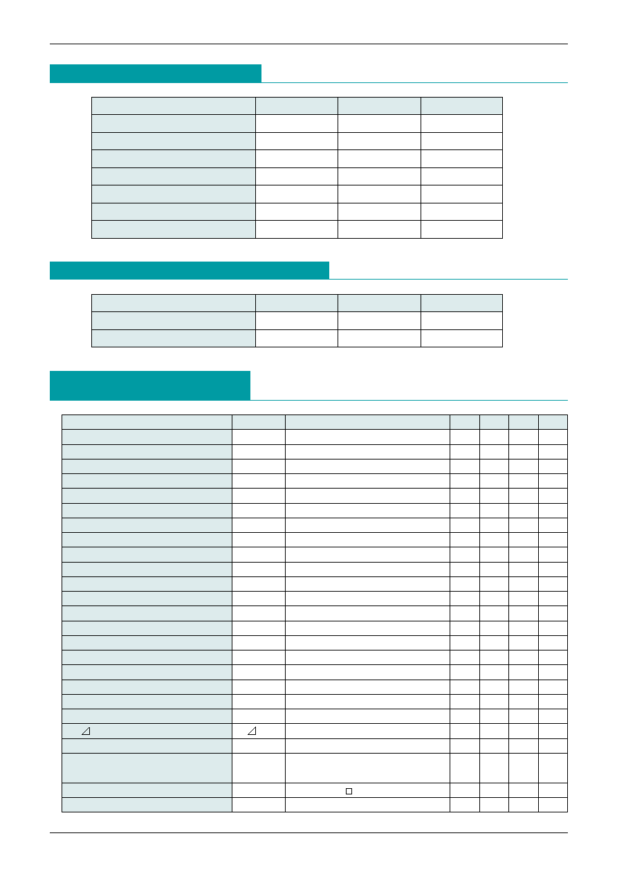
RGB Video Amplifier with OSD Input MM1381, 1382, 1383
Item
Symbol
Ratings
Units
Storage temperature
T
STG
-55~+150
°C
Power supply voltage
V
CC
max.
15.0
V
Input voltage range
V
IN
max.
GND <
= V
IN
<
= V
CC
V
Video output current
I
O
28
mA
Allowable loss
Pd
2.5
W
Electrostatic breakdown
2
kV
Pin temperature
265
*
16
°C
Absolute Maximum Ratings
*
1
Recommended Operating Conditions
*
2
Item
Symbol
Ratings
Units
Operating temperature
T
OPR
-20~+70
°C
Operating voltage
V
OPR
11.4~12.6
V
DC Electrical Characteristics
(Except where noted otherwise, Ta=25°C, V
CC
1=V
CC
2=12V,
V13=4V, V14=4V, V
DRV
=4V, V
CG
= 0V, V
BG
=4V, V4=0V, V
C
-o=1V)
*
3
Item
Symbol
Measurement conditions
Min. Typ. Max. Units
Consumption current
*
7
V
CC
V
CC
1+V
CC
2, R
L
=
95
120
mA
Video input resistance
R
IN
100
Clamp gate input voltage L
V
CGL
0.8
1.2
V
Clamp gate input voltage H
V
CGH
1.6
2.0
V
Clamp gate input current L
I
CGL
V
CG
=0V
-1.5
-5.0
uA
Clamp gate input current H
I
CGH
V
CG
=12V
0.01
1.0
uA
Blanking gate input voltage L
V
BGL
0.8
1.2
V
Blanking gate input voltage H
V
BGH
1.6
2.0
V
Blanking gate input current L
I
BGL
V
BG
=0V
-8
-11
uA
Blanking gate input current H
I
BGH
V
BG
=12V
0.01
1.0
uA
Reference voltage
V
REF
2.0
V
Input capacitor charging current
I
ICL+
V
CG
=0V
450
750
uA
Input capacitor discharge current
I
ICL-
V
CG
=0V
-450
750
uA
Input capacitor bias discharge current
I
ICLB
V
CG
=4V
±750
nA
Clamp cap charging current
I
OCL+
V
CG
=0V
450
750
uA
Clamp cap discharge current
I
OCL-
V
CG
=0V
-450 -750
uA
Clamp cap bias discharge current
I
OCLB
V
CG
=4V
750
nA
Output voltage L
V
OL
V
C
-
O
=0V
50
100
mV
Output voltage H
V
OH
V
C
-
O
=10V
7.0
7.5
V
Black level output voltage
V
O
V
C
-
O
=1V
*
7
1.2
V
Black level output voltage
V
O
V
C
-
O
=1V
±20
±250
mV
Output blanking voltage
V
OBLK
V
BG
=0V
100
500
mV
Contrast/drive input current
I13, 14
I26~28
V13=V14=V
DRV
=0V~4V
-125 -500
nA
Cutoff input current
I
C-O
V
-O
=0V~4V
-1.0
-1.5
uA
Spot killer voltage
V
SPOT
10.6
11.2
V
MITSUMI
RGB Video Amplifier with OSD Input MM1381, 1382, 1383
AC Electrical Characteristics
*
14
(Except where noted otherwise, Ta=25°C, V
CC
1=V
CC
2=12V, V13=4V, V14=4V, V
DRV
=4V,
V
CG
=0V, V
BG
=4V, V4=0V. For AC tests, adjust output pins 16, 20 and 23 to 4V by hand.)
Item
Symbol
Measurement conditions
Min. Typ. Max. Units
Video amp gain
A
V
max.
V13=4V, V
DRV
=4V
7.5
10.0
V/V
V
IN
=400mV
P-P
16.9
20.0
dB
Contrast attenuation 1
A
V
1
V13=2V
-6
dB
Contrast attenuation 2
A
V
2
V13=0.25V
-40
dB
Drive attenuation 1
A
VD
1
V
DRV
=2V
-4.5
dB
Drive attenuation 2
A
VD
2
V
DRV
=0.25V
-11
dB
Gain matching
A
VMAT
V13=V
DRV
=4V
*
8
±0.3
dB
Gain change between amps
A
VMAT
V13=4V~2V
*
9
±0.2
dB
Video amp distortion
THD
V
O
=1V
P-P
, f=10kHz
1
%
Video amp frequency bandwidth
f
BW
V13=4V, V
DRV
=3V
110
MHz
V
O
=4V
P-P
*
10, 11
Video output rise time
tr
V
O
=4V
P-P
*
10
3.0
nS
Video output fall time
tf
V
O
=4V
P-P
*
10
4.0
nS
Video amp isolation 1
V
SEP
1
V13=4V
*
12
-70
dB
Video amp isolation 2
V
SEP
2
V13=4V
*
10, 12
-50
dB
Blanking output rise time
tr
-BLK
V
O
=1V
P-P
*
10
8
nS
Blanking output fall time
tf
-BLK
V
O
=1V
P-P
*
10
14
nS
Blanking rise delay time
tr
D-BLK
V
O
=1V
P-P
23
nS
Blanking fall delay time
tf
D-BLK
V
O
=1V
P-P
20
nS
Back-porch clamping pulse width
tpw
*
13
200
nS
OSD Electrical Characteristics
(Except where noted otherwise, Ta = 25°C, V
CC
1=V
CC
2=12V,
V13=4V, V14=4V, V
DRV
=4V, V
CG
=4V, V
BG
=4V, V4=4V, V
C
-o=1V)
Item
Symbol
Measurement conditions
Min. Typ. Max. Units
Input voltage OSD L
V
OSDL
0.4
1.2
V
Input voltage OSD H
V
OSDH
1.6
2.0
V
OSD selection input voltage L
V4
L
0.8
1.2
V
OSD selection input voltage H
V4
H
1.6
2.0
V
OSD selection input current L
I4
L
V4=0V
-3.0
-5.0
uA
OSD selection input current H
I4
H
V4=12V
0.01
2.0
uA
OSD black level output voltage
V
OUT-OSD
V
C-O
=1V
±85
±175
mV
OSD output voltage V
P-P
V
OSD-O
V14=4V, V
DRV
=2V
4.5
V
P-P
OSD output V
P-P
attenuation
V
OSD-O
V14=2V, V
DRV
=2V
50
30
%
Output adjustment between channels
V
OSD-OMAT
V14=4V, V
DRV
=2V
±2.0
%
Output fluctuation between channels
V
OSD-OMAT
V14=4V~2V, V
DRV
=2V
±3.5
%
Video to OSD switching time
tr
-OSDSW
V1=V2=V3=4V
*
15
4
nS
OSD-to-video switching time
tr
-OSDSW
V1=V2=V3=4V
*
15
11
nS
Video to OSD transfer delay
tr
D-OSDSW
V1=V2=V3=V13=V14=4V
11
nS
OSD-to-video transport delay
tf
D-OSDSW
V1=V2=V3=V13=V14=4V
12
nS
OSD rise time
tr
-OSD
V14=4V
4
nS
OSD fall time
tf
-OSD
V14=4V
10
nS
OSD rise delay time
tr
D-OSD
V14=4V
6.5
nS
OSD fall delay time
tf
D-OSD
V14=4V
9
nS
Video isolation rate to OSD1
V
feed
1
V14=4V, V1=V2=V3=0V
-70
dB
Video isolation rate to OSD2
V
feed
2
V14=4V, V1=V2=V3=0V
-60
dB

MITSUMI
RGB Video Amplifier with OSD Input MM1381, 1382, 1383
Notes :
*
1
Absolute maximum ratings are the limits over which the device may be damaged.
*
2
Operating ratings are the conditions for device functioning, but they do not guarantee s
specific performance limit. Refer to the electrical characteristics section for guaranteed
specifications and measuring conditions. Guaranteed specifications apply only to the listed
conditions. If the device does not operate within the listed measuring conditions, there may be
deterioration depending on the performance characteristics.
*
3
V
CC
supply pins 6, 9 and 22 must be connected as one externally in order to prevent internal
damage during the V
CC
power supply on/switching cycle.
*
4
Human model. Discharge via 1.5k
from 100pF capacitor.
*
5
The typical specified value is +25°C, indicating the standard value of the most general
parameter.
*
6
The specified supply current is V
CC
1 and V
CC
2 0 input current for RL=[symbol]. Please refer to
the measuring circuit. V
CC
2 supply current also depends on output load. V
CC
2 load current is
8mA in the measuring circuit for video output of 1V DC.
*
7
Output voltage depends on the load resistor. The measuring circuit uses RL=390
.
*
8
Measure the gain difference between two amps. Vin=400mV
P-P
.
*
9
Measure Av max. attenuation, and measure the quantitative difference between any two amps.
*
10 Special test device on GND sealed PCB not requiring a socket.
*
11 Adjust input frequency from 10MHz (A
V
max. reference value) to -3dB corner frequency.
*
12 Measure the output level of two non-operational amps relative to the operating amp to check
channel separation.
*
13 200nS minimum pulse width is guaranteed to 15kHz horizontal line. This limit is guaranteed
at the design stage. When using a slower line speed, a clamp pulse with longer pulse width
is required.
*
14 4V DC level is the AC output signal center voltage for AC testing. For example, when output
is 4V
P-P
, the signal fluctuates between 2V DC and 6V DC.
*
15 trosd=11nS and tfosd=4ns for V1=V2=V4-0V and video input of 0.7V. The video output
waveform is the waveform shown in the timing diagram, inverted. Therefore, Trosd is actually
rise time, and Tfosd is actually fall time in this situation.
*
16 Solder for 10S.

MITSUMI
RGB Video Amplifier with OSD Input MM1381, 1382, 1383
Timing Diagram
Blanking transmission delay and Rise/fall time
OSD transmission delay and Rise/fall time
Video OSD, OSD Video transmission delay and Switching time
BLANK GATE
VIDEO OUT
VOH
VOL
0V
1V
tfD-BLK
tf-BLK
1.3V
0.5V
0.5V
1.3V
trD-BLK
tr-BLK
OSD IN
VIDEO/OSD
SWITCH
VIDEO OUT
VOH
VOL
VOH
1.3V
1.3V
VOL
trD-OSDS
tfD-OSDS
tf-OSDS
tr-OSDS
4V
P-P
1V
2V
2V
OSD IN
VIDEO/OSD
SWITCH
VIDEO OUT
VOH
VOL
VOH
VOL
1.3V
1.3V
1V
trD-OSD
tr-OSD
4V
P-P
2V
tfD-OSD
tf-OSD
2V
MITSUMI
RGB Video Amplifier with OSD Input MM1381, 1382, 1383
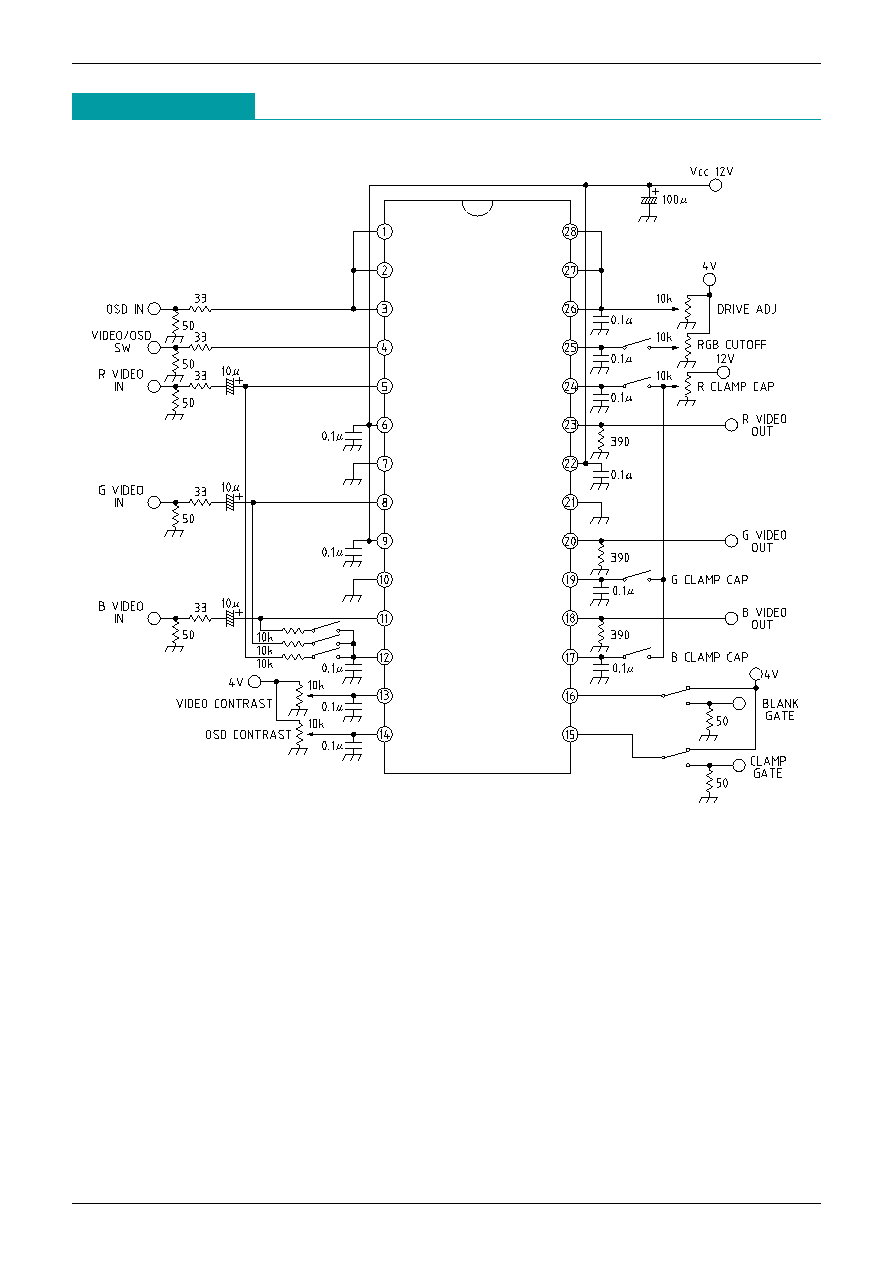
Measuring Circuit

MITSUMI
RGB Video Amplifier with OSD Input MM1381, 1382, 1383
Application Circuits