MITSUMI
System Reset (with battery back-up) MM1290
System Reset (battery back-up)
Monolithic IC MM1290
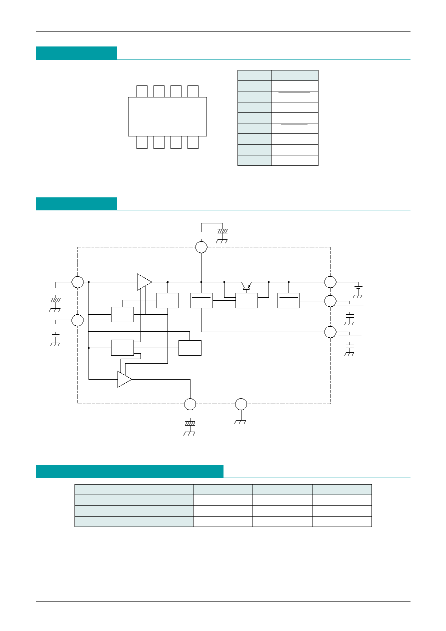
Outline
These ICs protect S-RAM data in back-up mode (CS signal makes S-RAM CE pin low and CE
-------------------------------------------
pin high) when
power supply voltage goes below a certain set voltage (detection voltage 4.6V typ.). Further, it switches from
main power supply to battery back-up when power supply voltage drops. Conversely, when power supply
rises, it first switches the S-RAM from battery back-up to main power supply (switching voltage 3.5V typ.),
then from back-up mode to normal mode (CS signal makes S-RAM CE pin high and CE pin low). These signal
processes provide reliable protection against data damage.
Features
1. Power supply switching circuit (switching between main power supply and battery)
2. CS control for S-RAM (normal mode : S-RAM can be accessed, back-up mode: S-RAM can not be
accessed low current consumption mode)
3. Back-up output V01 and V02 output circuit built in.
Characteristics
1. Battery back-up
1. Low IC current consumption (loss current)
2.7µA typ.
2. Drop voltage inside IC (input/output voltage difference)
I
O
=100µA
0.03V typ.
3. Reverse current (reverse leak current)
0.5µA max.
2. Normal operation
1. Drop voltage inside IC (input/output voltage difference)
I
O
=50mA
0.2V typ.
2. Output voltage
V
CC
=6V
I
O1
=50mA
5.0V typ.
3. Output voltage2
V
CC
=6V
I
O2
=30mA
5.0V typ.
3. Detection voltage
RESET
A : 2.55V typ.
PREEND
B : 2.70V typ.
Package
SOP-8A
Applications
1. Memory cards (S-RAM cards)
2. PCs, word processors
3. Fax machines, photocopiers, other office equipment
4. Sequence controllers, other FA equipment
5. Video games and other equipment with S-RAMs

MITSUMI
System Reset (with battery back-up) MM1290
Absolute Maximum Ratings
(Ta=25
°
C)
Item
Symbol
Rating
Unit
Power supply voltage 1
V
IN
max.
-0.3~+16
V
Power supply voltage2 (BACK UP)
V
BAT
max.
-0.3~+12
V
Pin Voltage
V
I
max.
-0.3~+10
V
Output current 1
I
O1
0~80
mA
Output current 2
I
O2
0~60
mA
Electrical Characteristics
(Except where noted otherwise, V
IN
=6.0, Ta=25°C)
Item
Symbol
Measurement conditions
Min. Typ. Max. Unit
Synthesis
Current consumption 1
I
IN
V
IN
=6V
40
80
µA
Current consumption 2
I
BAT1
V
BAT
=3V, V
IN
=6V
0.3
0.6
µA
Current consumption 3
I
BAT2
V
BAT
=3V Ta=25°C
2.7
4.5
µA
Regulator
Output voltage1
V
O1
V
IN
=6V, I
O1
=50mA
4.85
5.0
5.15
V
Input-Output differential Voltage1
V
IO1
V
IN
=6V, I
O1
=50mA
0.2
0.35
V
Load Regulation1
V
O1
I
O1
=0~50mA
±0.01 ±0.03 %/mA
Line Regulation1
V
I1
I
O1
=50mA
±0.01 ±0.2
%/V
V
OUT
Temperature Coefficient1
V
O1
Ta=-20~+75°C
±0.01
%/°C
Ta
Output voltage2
V
O2
V
IN
=V
O
+1V, I
O2
=30mA
4.85
5.0
5.15
V
Input-Output differential Voltage2
V
IO2
V
IN
=4.5V, I
O2
=30mA
0.2
0.35
V
Load Regulation2
V
O2
I
O2
=0~30mA
±0.01 ±0.03 %/mA
Line Regulation2
V
I2
I
O2
=30mA
±0.01 ±0.2
%/V
V
OUT
Temperature Coefficient2
V
O2
Ta=-20~+75°C
±0.01 ±0.20 %/°C
Ta
Reset
CS detection voltage
V
SL1
V
IN
=H L
4.485 4.600 4.715
V
Detection voltage temperature
V
g1
Ta=-20~+75°C
±0.01
%/°C
coefficient 1
Ta
CS sync current
I
SINK1
V
O
=0.5V, V
IN
=V
BAT
=2V
1.5
mA
CS operating voltage
V
OPL1
V
IN
or V
BAT
I
CS
=50µA, V
OP
=0.4V
1.6
16
V
RESET detection voltage
V
SL2
V
O1
=H L
2.499 2.550 2.601
V
RESET hysteresis
V
S2
V
O1
=H L H
45
90
180
mV
Detection voltage temperature
V
SL2
Ta=-20~+75°C
±0.01
%/°C
coefficient 2
Ta
RESET sync current
I
SINK2
V
OP
=0.4V, V
IN
=V
BAT
=2V
1.5
mA
PREEND detection voltage
V
SL3
V
BAT
=H L
2.646 2.700 2.754
V
PREEND hysteresis
V
S3
V
BAT
=H L H
110
140
250
mV
Detection voltage temperature
V
S3
Ta=-20~+75°C
±0.01
%/°C
coefficient 3
Ta
PREEND sync current
I
SINK3
V
OP
=0.4V, V
IN
=V
BAT
=2V
1.5
mA
RESET, PREEND operating voltage
V
OPL2
V
IN
or V
BAT
V
OP
=0.4V IR=IP=50µA
1.6
16
V

MITSUMI
System Reset (with battery back-up) MM1290
Electrical Characteristics
(Except where noted otherwise, V
IN
=6.0, Ta=25°C)
Item
Symbol
Measurement conditions
Min. Typ. Max. Unit
Switch
Switch voltage
V
SW1
V
BAT
=3V, V
IN
voltage detection
3.400 3.500 3.600
V
CS output prohibition voltage
V
SW2
V
BAT
=3V, V
O1
voltage detection
4.550 4.700 4.850
V
V
BAT
SW Leakage Current
I
LEAK
V
IN
=6V, V
BAT
=0V
0.5
µA
Input-Output differential Voltage
V
IOSW
V
IN
=OPEN, V
BAT
=2.65V, I
OUT
=100µA
30
60
mV
Switch Temperature Coefficient
V
SW1
Ta=-20~+75°C
±0.01
%/
°
C
Ta
CS voltage prohibition
V
SW2
Ta=-20~+75°C
±0.01
%/
°
C
Temperature Coefficient
Ta
(V) 5
0
RESET
(V) 5
0
PREEND
(V) 5
0
CS
(V) 5
0
V
BAT
(V) 5
0
V
O1
(V) 5
0
V
O2
(V) 5
0
V
IN
CS, PREEND RESET is pull-up to V
OUT
Timing Chart