Apr. 2004
MITSUBISHI <INTELLIGENT POWER MODULES>
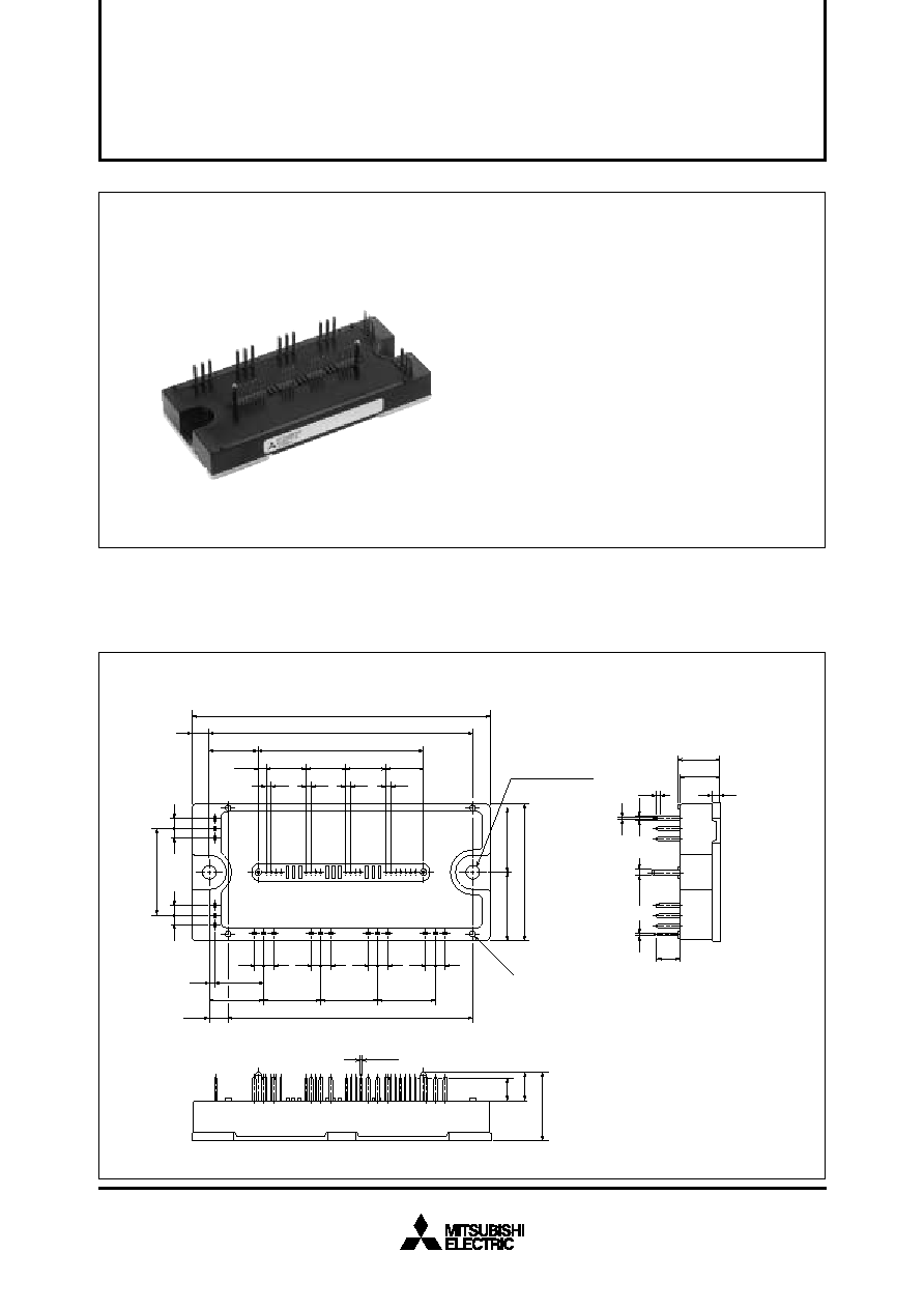
PM100RLB060
FLAT-BASE TYPE
INSULATED PACKAGE
PM100RLB060
FEATURE
a) Adopting new 5th generation IGBT (CSTBT) chip, which
performance is improved by 1
µ
m fine rule process.
For example, typical V
ce
(sat)=1.5V @Tj=125
°
C
b) I adopt the over-temperature conservation by Tj detection of
CSTBT chip, and error output is possible from all each con-
servation upper and lower arm of IPM.
c) New small package
Reduce the package size by 32%, thickness by 22% from
S-DASH series.
d) Current rating of brake part increased.
50% for the current rating of inverter part.
· 3
100A, 600V Current-sense IGBT type inverter
· 50A, 600V Current-sense regenerative brake IGBT
· Monolithic gate drive & protection logic
· Detection, protection & status indication circuits for, short-
circuit, over-temperature & under-voltage (P-Fo available
from upper arm devices)
· Acoustic noise-less 11kW class inverter application
APPLICATION
General purpose inverter, servo drives and other motor controls
PACKAGE OUTLINES
Dimensions in mm
22
7.75
98.25
2.5
23
23
23
19.5
25.75
25
55
17
16
3
19-
s
0.5
9.5
11.5
27.5
9.5
1
1
1.5
1.5
2-
2.5
106
±
0.25
66.5
19.75
3.25
7
4
4
35
4
4
4
4
4
4
4
4
4
4
16
15.25
6-2
3-2
3-2
3-2
16
16
120
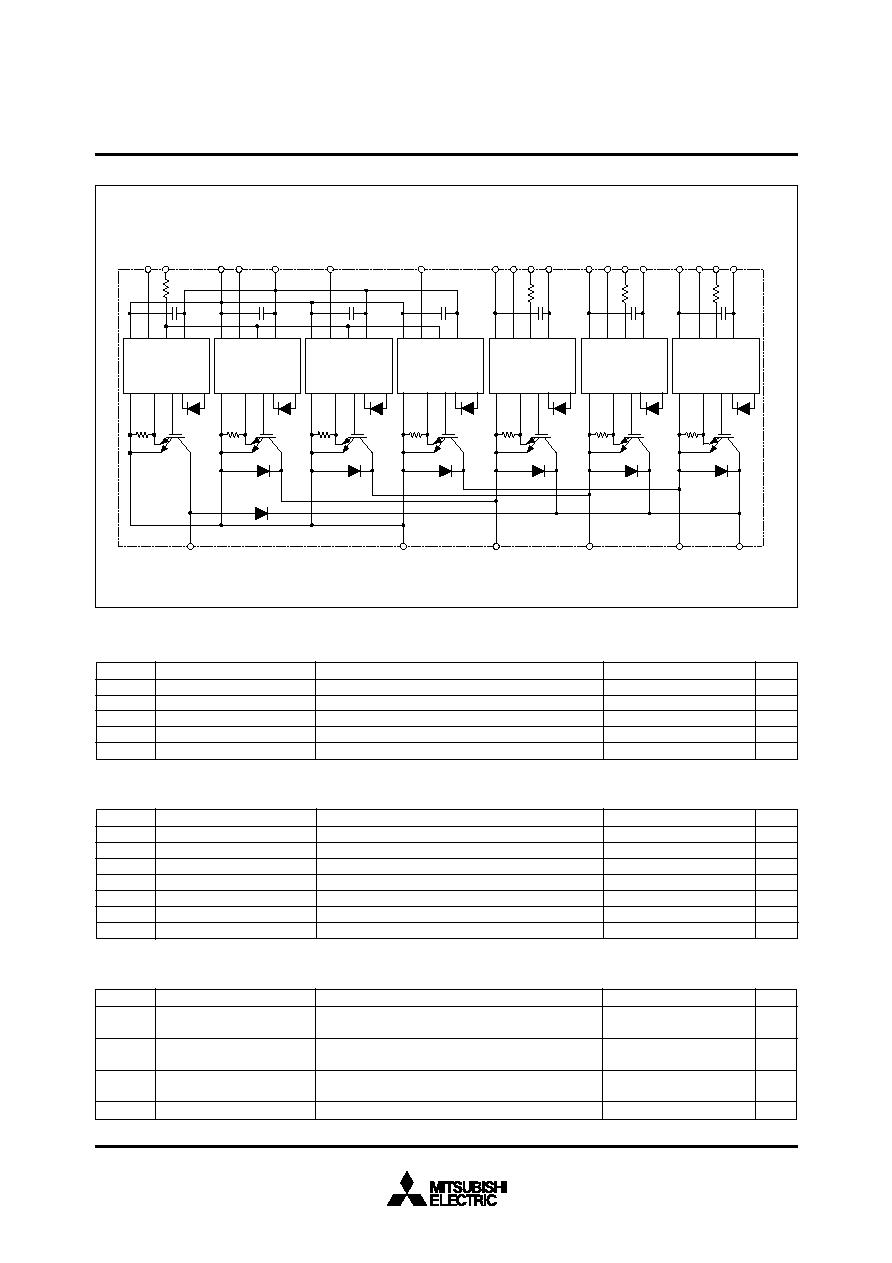
1. VUPC
2. UFO
3. UP
4. VUP1
5. VVPC
6. VFO
7. VP
8. VVP1
9. VWPC
10. WFO
11. WP
12. VWP1
13. VNC
14. VN1
15. Br
16. UN
17. VN
18. WN
19. Fo
Terminal code
NP
1
5
B
U
V
W
9
13
19
4-
2.5
MOUNTING HOLES
2-
5.5
MITSUBISHI <INTELLIGENT POWER MODULES>
PM100RLB060
FLAT-BASE TYPE
INSULATED PACKAGE
Apr. 2004
V
CES
±
I
C
±
I
CP
P
C
T
j
Collector-Emitter Voltage
Collector Current
Collector Current (Peak)
Collector Dissipation
Junction Temperature
V
D
= 15V, V
CIN
= 15V
T
C
= 25
°
C
T
C
= 25
°
C
T
C
= 25
°
C
(Note-1)
V
A
A
W
°
C
MAXIMUM RATINGS (Tj = 25
°
C, unless otherwise noted)
INVERTER PART
Symbol
Parameter
Condition
Ratings
Unit
600
100
200
356
20 ~ +150
INTERNAL FUNCTIONS BLOCK DIAGRAM
V
CES
I
C
I
CP
P
C
V
R(DC)
I
F
T
j
BRAKE PART
Collector-Emitter Voltage
Collector Current
Collector Current (Peak)
Collector Dissipation
FWDi Rated DC Reverse Voltage
FWDi Forward Current
Junction Temperature
V
D
= 15V, V
CIN
= 15V
T
C
= 25
°
C
T
C
= 25
°
C
T
C
= 25
°
C
(Note-1)
T
C
= 25
°
C
T
C
= 25
°
C
V
A
A
W
V
A
°
C
Symbol
Parameter
Condition
Ratings
Unit
600
50
100
228
600
50
20 ~ +150
V
FO
I
FO
CONTROL PART
V
mA
20
20
Supply Voltage
Input Voltage
Fault Output Supply Voltage
Fault Output Current
Symbol
Parameter
Condition
Ratings
Unit
Applied between : V
UP1
-V
UPC
V
VP1
-V
VPC
, V
WP1
-V
WPC
, V
N1
-V
NC
Applied between : U
P
-V
UPC
, V
P
-V
VPC
W
P
-V
WPC
, U
N
· V
N
· W
N
· B
r
-V
NC
Applied between : U
FO
-V
UPC
, V
FO
-V
VPC
, W
FO
-V
WPC
F
O
-V
NC
Sink current at U
FO
, V
FO
, W
FO
, F
O
terminals
20
20
V
D
V
CIN
V
V
V
N
U
N
W
P
V
WP1
WF
O
V
WPC
V
P
V
VP1
VF
O
V
VPC
U
P
V
UP1
UF
O
V
UPC
Br
B
N
W
V
U
P
Fo
V
NC
V
N1
W
N
Gnd In
Fo Vcc
Gnd
Si Out
OT
Gnd In
Fo Vcc
Gnd
Si Out
OT
Gnd In
Fo Vcc
Gnd
Si Out
OT
Gnd In
Fo Vcc
Gnd
Si Out
OT
Gnd In
Fo Vcc
Gnd
Si Out
OT
Gnd In
Fo Vcc
Gnd
Si Out
OT
Gnd In
Fo Vcc
Gnd
Si Out
OT
MITSUBISHI <INTELLIGENT POWER MODULES>
PM100RLB060
FLAT-BASE TYPE
INSULATED PACKAGE
Apr. 2004
Parameter
Symbol
Supply Voltage Protected by
SC
Supply Voltage (Surge)
Module Case Operating
Temperature
Storage Temperature
Isolation Voltage
Condition
V
CC(surge)
T
C
T
stg
V
iso
Ratings
V
CC(PROT)
400
500
20 ~ +100
40 ~ +125
2500
Unit
V
°
C
°
C
V
rms
V
V
D
= 13.5 ~ 16.5V, Inverter Part,
T
j
= +125
°
C Start
Applied between : P-N, Surge value
(Note-1)
60Hz, Sinusoidal, Charged part to Base, AC 1 min.
(Note-1) Tc (base plate) measurement point is below.
2.1
2.0
3.3
2.4
0.4
1.0
2.5
1.0
1
10
Min.
Typ.
Max.
Collector-Emitter
Saturation Voltage
Collector-Emitter
Cutoff Current
I
C
= 100A, V
D
= 15V, V
CIN
= 15V
(Fig. 2)
T
j
= 25
°
C
T
j
= 125
°
C
ELECTRICAL CHARACTERISTICS (Tj = 25
°
C, unless otherwise noted)
INVERTER PART
Parameter
Symbol
Condition
V
CE(sat)
I
CES
V
EC
t
on
t
rr
t
c(on)
t
off
t
c(off)
Limits
--
--
--
0.5
--
--
--
--
--
--
1.6
1.5
2.2
1.0
0.2
0.4
1.2
0.5
--
--
T
j
= 25
°
C
T
j
= 125
°
C
FWDi Forward Voltage
Switching Time
V
D
= 15V, V
CIN
= 0V
15V
V
CC
= 300V, I
C
= 100A
T
j
= 125
°
C
Inductive Load
(Fig. 3,4)
V
CE
= V
CES
, V
CIN
= 15V
(Fig. 5)
V
D
= 15V, I
C
= 100A
V
CIN
= 0V, Pulsed
(Fig. 1)
TOTAL SYSTEM
V
mA
V
µ
s
Unit
0.27*
0.43*
0.42*
0.71*
0.35
0.56
0.55
0.92
0.038
°
C/W
R
th(j-c)Q
R
th(j-c)F
R
th(j-c)Q
R
th(j-c)F
R
th(j-c)Q
R
th(j-c)F
R
th(j-c)Q
R
th(j-c)F
R
th(c-f)
Inverter IGBT part (per 1/6)
(Note-2)
Inverter FWDi part (per 1/6)
(Note-2)
Brake IGBT part
(Note-2)
Brake FWDi part
(Note-2)
Inverter IGBT part (per 1/6)
(Note-1)
Inverter FWDi part (per 1/6)
(Note-1)
Brake IGBT part
(Note-1)
Brake FWDi part
(Note-1)
Case to fin, (per 1 module)
Thermal grease applied
(Note-1)
Symbol
Condition
Unit
Min.
--
--
--
--
--
--
--
--
--
--
--
--
--
--
--
--
--
--
Junction to case Thermal
Resistances
THERMAL RESISTANCES
Contact Thermal Resistance
Parameter
Limits
Typ.
Max.
UP
IGBT
28.3
8.5
VP
WP
UN
VN
WN
Br
FWDi
28.0
1.7
IGBT
65.0
8.5
FWDi
65.2
1.7
IGBT
87.0
8.5
FWDi
87.2
1.7
IGBT
39.3
6.5
FWDi
39.5
5.2
IGBT
54.0
6.5
FWDi
53.7
5.2
IGBT
76.0
6.5
FWDi
75.7
5.2
IGBT
17.5
10.4
FWDi
18.7
4.0
arm
axis
X
Y
Bottom view
NP
B
U
V
W
Top view
Tc
* If you use this value, R
th(f-a)
should be measured just under the chips.
(Note-2) Tc (under the chip) measurement point is below.
(unit : mm)

MITSUBISHI <INTELLIGENT POWER MODULES>
PM100RLB060
FLAT-BASE TYPE
INSULATED PACKAGE
Apr. 2004
3.5
--
--
--
Mounting part
screw : M5
--
Symbol
Parameter
Mounting torque
Weight
Condition
Unit
N · m
g
Limits
Min.
Typ.
Max.
2.5
--
3.0
340
MECHANICAL RATINGS AND CHARACTERISTICS
--
--
--
--
--
V
CE(sat)
I
CES
V
FM
V
mA
Min.
Typ.
Max.
V
Collector-Emitter
Saturation Voltage
FWDi Forward Voltage
Collector-Emitter
Cutoff Current
I
F
= 50A
(Fig. 2)
T
j
= 25
°
C
T
j
= 125
°
C
Unit
Parameter
Symbol
Condition
Limits
2.1
2.0
3.3
1
10
1.6
1.5
2.2
--
--
T
j
= 25
°
C
T
j
= 125
°
C
BRAKE PART
V
D
= 15V, I
C
= 50A
V
CIN
= 0V, Pulsed
(Fig. 1)
V
CE
= V
CES
, V
CIN
= 15V
(Fig. 5)
V
D
= 15V, V
CIN
= 15V
Applied between : U
P
-V
UPC
, V
P
-V
VPC
, W
P
-V
WPC
U
N
· V
N
· W
N
· B
r
-V
NC
I
D
°
C
V
mA
ms
30
10
1.8
2.3
--
--
--
--
--
12.5
--
0.01
15
--
mA
Circuit Current
Input ON Threshold Voltage
Input OFF Threshold Voltage
Short Circuit Trip Level
Short Circuit Current Delay
Time
Over Temperature Protection
Supply Circuit Under-Voltage
Protection
Fault Output Current
Minimum Fault Output Pulse
Width
V
th(ON)
V
th(OFF)
SC
t
off(SC)
OT
OT
r
UV
UV
r
I
FO(H)
I
FO(L)
t
FO
Trip level
Reset level
Trip level
Reset level
CONTROL PART
--
--
1.2
1.7
200
100
--
135
--
11.5
--
--
--
1.0
Parameter
Symbol
Condition
Max.
Min.
Typ.
Unit
Limits
20
5
1.5
2.0
--
--
0.2
145
125
12.0
12.5
--
10
1.8
(Note-3) Fault output is given only when the internal SC, OT & UV protections schemes of either upper or lower arm device operate to
protect it.
V
D
= 15V
Detect Tj of IGBT chip
20
T
j
125
°
C
V
D
= 15V, V
FO
= 15V
(Note-3)
V
D
= 15V
(Note-3)
V
µ
s
V
N1
-V
NC
V
XP1
-V
XPC
Inverter part
Brake part
A
RECOMMENDED CONDITIONS FOR USE
Recommended value
Unit
Condition
Symbol
Parameter
V
Applied across P-N terminals
Applied between : V
UP1
-V
UPC
, V
VP1
-V
VPC
V
WP1
-V
WPC
, V
N1
-V
NC
(Note-4)
Applied between : U
P
-V
UPC
, V
P
-V
VPC
, W
P
-V
WPC
U
N
· V
N
· W
N
· B
r
-V
NC
Using Application Circuit of Fig. 8
For IPM's each input signals
(Fig. 7)
Supply Voltage
Control Supply Voltage
Input ON Voltage
Input OFF Voltage
PWM Input Frequency
Arm Shoot-through
Blocking Time
400
15
±
1.5
0.8
9.0
20
2.0
V
CC
V
CIN(ON)
V
CIN(OFF)
f
PWM
t
dead
V
D
V
kHz
µ
s
V
(Note-4) With ripple satisfying the following conditions dv/dt swing
±
5V/
µ
s, Variation
2V peak to peak
20
T
j
125
°
C, V
D
= 15V (Fig. 3,6)
V
D
= 15V
(Fig. 3,6)
MITSUBISHI <INTELLIGENT POWER MODULES>
PM100RLB060
FLAT-BASE TYPE
INSULATED PACKAGE
Apr. 2004
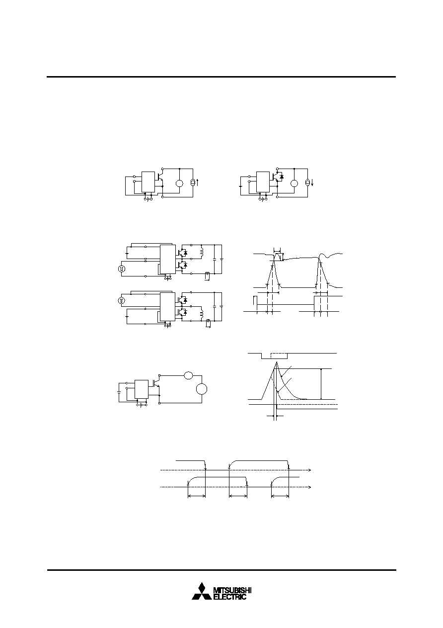
PRECAUTIONS FOR TESTING
1. Before appling any control supply voltage (V
D
), the input terminals should be pulled up by resistores, etc. to their corre-
sponding supply voltage and each input signal should be kept off state.
After this, the specified ON and OFF level setting for each input signal should be done.
2. When performing "SC" tests, the turn-off surge voltage spike at the corresponding protection operation should not be al-
lowed to rise above V
CES
rating of the device.
(These test should not be done by using a curve tracer or its equivalent.)
P, (U,V,W,B)
U,V,W, (N)
U,V,W,B, (N)
V
D
(all)
IN
Fo
IN
Fo
V
D
(all)
V
CIN
(0V)
Ic
V
V
P, (U,V,W)
V
CIN
(15V)
Ic
Fig. 7 Dead time measurement point example
Fig. 1 V
CE(sat)
Test
Fig. 2 V
EC
, (V
FM
) Test
0V
1.5V
1.5V
1.5V
2V
2V
2V
0V
t
t
t
dead
t
dead
t
dead
1.5V: Input on threshold voltage Vth(on) typical value, 2V: Input off threshold voltage Vth(off) typical value
IPM' input signal V
CIN
(Upper Arm)
IPM' input signal V
CIN
(Lower Arm)
10%
90%
trr
Irr
tr
td(on)
tc(on)
tc(off)
td(off)
V
CIN
Ic
V
CE
10%
10%
10%
90%
tf
(ton= td(on) + tr)
(toff= td(off) + tf)
Fo
Fo
P
N
N
C
S
C
S
U,V,W
Vcc
Vcc
Ic
Ic
V
D
(all)
V
D
(all)
P
U,V,W
V
CIN
V
CIN
V
CIN
(15V)
V
CIN
(15V)
Fo
Fo
Fig. 3 Switching time and SC test circuit
Fig. 4 Switching time test waveform
a) Lower Arm Switching
Signal input
(Upper Arm)
Signal input
(Lower Arm)
Signal input
(Upper Arm)
Signal input
(Lower Arm)
b) Upper Arm Switching
V
CIN
Fig. 5 I
CES
Test
Fig. 6 SC test waveform
SC
Short Circuit Current
toff(SC)
V
D
(all)
U,V,W, (N)
P, (U,V,W,B)
A
Pulse
V
CE
V
CIN
(15V)
Ic
Fo
IN
Fo
Constant Current