
MITSUBISHI (OPTICAL DEVICES)
MF-156DF-T12-20x/29x/23x
MF-156DS-R13-17x
SONET/SDH TRANSMITTER & RECIEVER
DESCRIPTION
This product is designed to provide high optical
performance for SDH STM-1/SONET OC-3.
Transmitter uses uncooled laser in a hermetic pigtail
coaxial module with drivered by specific integrated
circuit.
Receiver uses PIN preamp in a hermetic pigtail
coaxial module and integrated circuits for reshaping,
retiming and regenerating optical signal.
FEATURES
SONET,SDH system from intra-office to long-
leach application fully line up
Low cost and Low power consumption
Multisourced 20-Pin DIP with pigtail fiber
Single +5V power supply and P-ECL compatible
input and output
Operating case temperature range -40 to 85
°
C
With clock recovery and digital alarm function
APPLICATION
Short haul and long haul telecommunication systems
for SDH STM-1 / SONET OC-3.
ABSOLUTE MAXIMUM RATINGS
Stress below listed absolute maximum rating may cause permanent damage to the module.
Th is is a stress o nly and functional operation of the module at these or any other conditions in excess of those
given in the operational sections of this data sheet.
Exposure to Absolute Maximum Rating for extended periods may affect module reliability.
(T
C
=25
°
C)
Parameters
Symbol
Ratings
Unit
Supply voltage
Vcc
+6 to 0
V
PECL high output current
-
-50 to 0
mA
PECL input voltage
-
0 to Vcc+0.4
V
Storage temperature
Tstg
-40 to 85
°
C
Operating case temperature
Tc
-40 to 85
°
C
Soldering Temperature
-
+260
°
C
Soldering Time
-
10
sec
Relative humidity(non condensation)
-
10 to 80
%
Fiber bend radius from package
rF
32
mm

MITSUBISHI (OPTICAL DEVICES)
MF-156DF-T12-20x/29x/23x
MF-156DS-R13-17x
SONET/SDH TRANSMITTER & RECIEVER
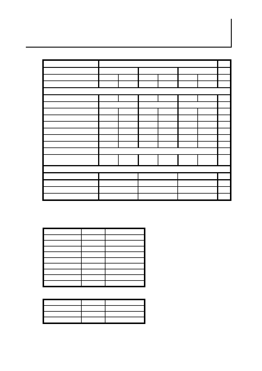
ELECTRICAL CHARACTERISTICS
All parameters are specified over the operating case temperature.
Measurement conditions are at 155.52Mb/s+/-20ppm, NRZ PN2
23
-1 and 50% duty cycle data signal.
The DATA input/output and CLOCK output signal levels are PECL compatible.
The transmitter disable input signal level is CMOS/TTL compatible.
The Signal Detect output signal level is PECL level compatible.
Transmitter
Parameters
Condition
Symbol
Min.
Typ.
Max.
Unit
Supply voltage
-
Vcc
4.75
5.0
5.25
V
Power consumption
-
Pc
-
0.5
1.3
W
PECL input voltage
note 1
-
PECL
-
Transmitter Disable voltage
note 2
Vd
Vcc-2.0V
-
Vcc
V
Transmitter Enable voltage
note 2
Ve
0
-
0.8
V
Laser bias monitor voltage
note 3
Vb
0.01
-
0.45
V
Laser backface monitor voltage
note 3
Vbf
0.01
-
0.20
V
Receiver
Parameters
Condition
Symbol
Min.
Typ.
Max.
Unit
Supply voltage
-
Vcc
4.75
5.0
5.25
V
Power consumption
-
Pc
-
1.0
1.5
W
PECL input voltage
note 4,5
-
PECL
-
Data/Clock external Load
note 4
RI
50
ohm
Data to clock phase
note 6
Tcda
-800
-
800
psec.
Clock duty
note 6
-
45
-
55
%
Jitter
-
-
ITU Rec.compliant
-
Signal Detect Response Time:
Decreasing Light Input
note 5,7
SDRTd
-
-
100
us
Signal Detect Response Time:
Increasing Light Input
note 5,7
SDRTi
-
-
100
us
Photo Bias Current Responsity
note 8
PBr
0.6
-
-
A/W
MITSUBISHI (OPTICAL DEVICES)
MF-156DF-T12-20x/29x/23x
MF-156DS-R13-17x
SONET/SDH TRANSMITTER & RECIEVER
OPTICAL CHARACTERISTICS
Parameter
Specification
Unit
ITU code
S-1.1
L-1.1
L-1.2
Min.
Max.
Min.
Max.
Min.
Max.
Optical Budget
0
14
0
29
0
30
dB
Transmitter
Wavelength
1261
1360
1280
1335
1480
1580
nm
Optical source
MLM
SLM(MLM)
SLM
-
Optical power at pigtail
-14
-8
-5
0
-4
0
dBm
Optical power when disable
-
-45
-
-45
-
-45
dBm
Spectral width(rms)
-
4
-
-(4)
-
-
nm
Spectral width(-20dB)
-
-
-
1(-)
-
1
nm
SMSR
-
-
30(-)
-
30
-
dB
Extinction ratio
8.2
-
10
-
10
-
dB
Optical wave form
SONET/SDH Mask compliant
-
Path penalty
(dispersion = ITU-T compliant)
-
1
-
1
-
1
dB
Receiver
Min.
Typ.
Max.
Wavelength
1260
-
1580
nm
Sensitivity
-
-36
-34
dBm
Overload
0
+1
-
dBm
ORDERING INFORMATION
Transmitter
Part number
ITU-code
Optical connector type
MF-156DF-T12-200
S-1.1
FC
MF-156DF-T12-201
S-1.1
SC
MF-156DF-T12-202
S-1.1
ST
MF-156DF-T12-290
L-1.1
FC
MF-156DF-T12-291
L-1.1
SC
MF-156DF-T12-292
L-1.1
ST
MF-156DF-T12-230
L-1.2
FC
MF-156DF-T12-231
L-1.2
SC
MF-156DF-T12-232
L-1.2
ST
Receiver
Part number
ITU-code
Optical connector type
MF-156DS-R13-170
STM-1
FC
MF-156DS-R13-171
STM-1
SC
MF-156DS-R13-172
STM-1
ST

MITSUBISHI (OPTICAL DEVICES)
MF-156DF-T12-20x/29x/23x
MF-156DS-R13-17x
SONET/SDH TRANSMITTER & RECIEVER
BLOCK DIAGRAM
OPT.OUT
DATA IN
DATA IN
Laser-bias monitor(-)
Transmitter disable
Laser-bias monitor(+)
Laser-backface
monitor(-)
Laser-backface
monitor(+)
DRIVER IC
LD Module
Transmitter Block Diagram
A.P.C.
Curcuit
Driver
IC
PD
LD
Integrated device
Clock recovery IC
Limiting IC
OPT.IN
CLK Out
CLK Out
DATA Out
DATA Out
Signal Detect
Receiver Block Diagram
PLL
Decider
Alarm
PD-Preamp
Module
Rt
Amp
Preamp
PD

MITSUBISHI (OPTICAL DEVICES)
MF-156DF-T12-20x/29x/23x
MF-156DS-R13-17x
SONET/SDH TRANSMITTER & RECIEVER
TRANSMITTER PIN ALLOCATION
No.
Symbol
Description
No.
Symbol
Description
1
NC
No user connection
20
NC
No user connection
2
Lbs(+)
Laser-bias monitor(+)
19
Lbf(+)
Laser-backface monitor(+)
3
NC
No user connection
18
Vcc
Vcc
4
Lbs(-)
Laser-bias monitor(-)
17
Lbf(-)
Laser-backface monitor(-)
5
GND
Ground
16
Data
Data
6
Vcc
Vcc
15
Data
Data
7
Td
Transmitter disable
14
GND
Ground
8
Vcc
Vcc
13
GND
Ground
9
Vcc
Vcc
12
Vcc
Vcc
10
NC
No user connection
11
GND
Ground
TRANSMITTER PIN DESCRIPTIONS
Pin No.
Function
I/O
Pin description
5,11,
13,14
GND
I
These pin are the module's ground connections.
They should be connected to a low inpedance ground plane(0V).
6,8,9,
12,18
Vcc
I
This is the power supply pin for the module.
It should be connected to +5.0V.
Recommended power supply decoupling.
15,16
Data & Data
I
This data input pin modulates the laser diode. When the Dat a input is
asserted,the laser diode is turned on.
Signal level of these pin are PECL level and internal Vbb bias. Refer t o
electrical interface in NOTE1.
7
Transmitter disable
I
The transmitt er is nomally enabled and only requires an external voltage
to disable.
Refer to electrical interface in NOTE2.
2,4
Laser-bias
monitor(+),
Laser-bias monitor(-)
O
The laser bias current is calculat ed as a rat io of the volt age to an int ernal
10 ohm sensing resistor.
Ib[mA]={Lbs(+)-Lbs(-)}[mV]/10
Refer to electrical interface in NOTE3.
17,19
Laser-backface
monitor(+),
Laser-backface
monitor(-)
O
The laser backface monitor is calculated as a ratio of t he voltage to an
internal 200 ohm sensing resistor.
Ibf[mA]={Lbf(+)-Lbf(-)}[mV]/200
Refer to electrical interface in NOTE3.
1,3,
10,20
NC
-
These pin are No user connection and should be left open.