MITSUBISHI
DIGITAL ASSP
M66222SP/FP
128
×
8-BIT
×
2 MAIL-BOX
1
DESCRIPTION
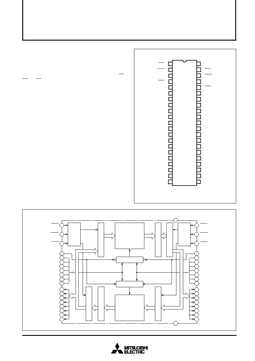
The M66222 is a mail box that incorporates two complete CMOS
shared memory cells of 128
×
8-bit configuration using high-
performance silicon gate CMOS process technology, and are
equipped with two access ports of A and B.
Access ports A and B are equipped with independent addresses CS,
WE and OE control pins and I/O pins to allow independent and
asynchronous read/write operations individually. This product
exclusively performs a write operation from A port and a read operation
from B port for one memory, and a read operation from A port and a
write operation from B port for the other memory.
FEATURES
· Memory configuration of 128
×
8 bits
×
2 memory areas
· High-speed access, address access time 40ns (typ.)
· Complete asynchronous accessibility from ports A and B
· Fixed read/write access ports for memory
· Completely static operation
· Low power dissipation CMOS design
· 5V single power supply
· TTL direct-coupled I/O
· 3-state output for I/O pins
APPLICATION
Inter-MCU data transfer memory, communication buffer memory
MITSUBISHI
DIGITAL ASSP
M66222SP/FP
128
×
8-BIT
×
2 MAIL-BOX
BLOCK DIAGRAM
PIN CONFIGURATION (Top view)
41
40
38
30
37
36
35
34
33
32
31
22
23
24
25
26
27
28
29
1
2
4
12
5
6
7
8
9
10
11
13
14
15
16
17
18
19
20
42
21
READ/
WRITE
CONTROL
CIRCUIT
MEMORY AREA(1)
128-WORD
×
8-BIT
CONFIGURATION
0-127
ADDRESSES
SENSE AMPLIFIER
OUTPUT BUFFER
READ/
WRITE
CONTROL
CIRCUIT
ROW/COLUMN
DECODER
ROW/COLUMN
DECODER
MEMORY AREA(2)
128-WORD
×
8-BIT
CONFIGURATION
128-255
ADDRESSES
OUTPUT BUFFER
SENSE AMPLIFIER
INPUT DATA CONTROL
CIRCUIT
INPUT DATA CONTROL
CIRCUIT
Write
Read
A
0
A~A
6
A
A
0
B~A
6
B
V
CC
GND
CSA
WEA
OEA
A
7
A
A
0
A
A
1
A
A
2
A
A
3
A
A
4
A
A
5
A
A
6
A
I/O
0
A
I/O
1
A
I/O
2
A
I/O
3
A
I/O
4
A
I/O
5
A
I/O
6
A
I/O
7
A
CSB
WEB
OEB
A
7
B
A
0
B
A
1
B
A
2
B
A
3
B
A
4
B
A
5
B
A
6
B
I/O
0
B
I/O
1
B
I/O
2
B
I/O
3
B
I/O
4
B
I/O
5
B
I/O
6
B
I/O
7
B
CHIP SELECT
INPUT
WRITE
ENABLE INPUT
OUTPUT
ENABLE INPUT
A PORT
ADDRESS
INPUT
A PORT
DATA I/O
CHIP
SELECT INPUT
WRITE
ENABLE INPUT
OUTPUT
ENABLE INPUT
B PORT
ADDRESS
INPUT
B PORT
DATA I/O
Read
Write
7
7
CSA
1
2
3
4
5
6
7
8
9
10
11
12
13
14
15
16
17
18
19
20
21
25
24
23
22
27
26
29
28
31
30
35
34
33
32
37
36
39
38
41
40
42
WEA
NC
OEA
I/O
7
A
GND
I/O
6
A
I/O
5
A
I/O
4
A
I/O
3
A
I/O
2
A
I/O
1
A
I/O
0
A
A
7
A
A
6
A
A
5
A
A
4
A
A
3
A
A
2
A
A
1
A
A
0
A
CSB
V
CC
NC
WEB
A
0
B
OEB
A
1
B
A
2
B
A
3
B
A
4
B
A
5
B
I/O
7
B
A
6
B
A
7
B
I/O
6
B
I/O
5
B
I/O
4
B
I/O
3
B
I/O
2
B
I/O
1
B
I/O
0
B
CHIP SELECT
INPUT
WRITE ENABLE
INPUT
OUTPUT ENABLE
INPUT
A PORT
ADDRESS
INPUT
A PORT
DATA I/O
CHIP SELECT
INPUT
WRITE ENABLE
INPUT
OUTPUT ENABLE
INPUT
B PORT
ADDRESS
INPUT
B PORT
DATA I/O
Outline
NC: No Connection
42P4B
42P2R-A
M66222SP/FP
MITSUBISHI
DIGITAL ASSP
M66222SP/FP
128
×
8-BIT
×
2 MAIL-BOX
2
FUNCTION
The M66222 is a mail box most suitable for inter-MCU data
communication interface. Provision of two pairs of addresses and
data buses in its shared memory cell of 128
×
8-bit configuration
allows independent and asynchronous read/write operations from/to
two access ports of A and B individually.
Two memory areas of 128
×
8-bit configuration are incorporated in
the chip. Memory area (1) is used only to perform a write operation
from A port and a read operation from B port, and memory area (2)
only to perform a read operation from A port and a write operation
from B port.
In this case, address A
7
A should be set to "L" when writing data from
A port in memory area (1), and address A
7
B should be set to "L"
when reading data from B port in memory area (1). Also, address
A
7
B should be set to "H" when writing data from B port in memory
area (2), and address A
7
A should be set to "H" when reading data
from A port in memory area (2).
Therefore, an attempt to set addresses A
7
A and A
7
B from each port
in a mode other than the above setting invalidates any read/write
operation from the corresponding port (See Table 1 and Fig 1).
As a basic write operation to memory, one of addresses A
0
to A
7
is
specified. The CS signal is set to "L" to place one of I/O pins in the
input mode. Also, the WE signal is set to "L". Data at the I/O pin is
written into memory.
As a read operation, the WE signal is set to "H". Both CS signal and
OE signal are set to "L" to place one of I/O pins in the output mode.
One of addresses A
0
to A
7
is specified. Data at the specified address
is thus output to the I/O pin.
When the CS signal is set to "H", the chip enters a non-select state
which inhibits a read and write operation. At this time, the output is
placed in the floating state (high impedance state), thus allowing OR
tie with another chip. When the OE signal is set to "H", the output
enters the floating state. In the I/O bus mode, setting the OE signal
to "H" at a write time avoids contention of I/O bus data. When the CS
signal is set to Vcc, the output enters the full stand-by state to minimize
supply current (See Tables 2 and 3).
Access
port
Operation
A port
A
7
A = "L"
A
7
A = "H"
B port
A
7
B = "H"
A
7
B = "L"
Write
Read
Note 1: No input data is written into any port having address A
7
set under
any condition other than Table 1. Undefined data is read to an
output pin during a read operation.
Fig 1 Access from Ports
Table 2 A Port Function Table
CSA
L
L
L
H
WEA
L
H
H
×
OEA
×
L
H
×
A
7
A
L
H
L
H
×
×
Mode
Write
Invalid
Invalid
Read
--
Non-select
I/O pin
D
IN
D
IN
D
OUT
D
OUT
High impedance
High impedance
I
CC
Operation
Operation
Operation
Operation
Operation
Stand-by
Note 2:
×
indicates "L" or "H". (Irrelevant)
"H" = High level, "L" = Low level
Table 3 B Port Function Table
CSB
L
L
L
H
WEB
L
H
H
×
OEB
×
L
H
×
A
7
B
L
H
L
H
×
×
Mode
Invalid
Write
Read
Invalid
--
Non-select
I/O pin
D
IN
D
IN
D
OUT
D
OUT
High impedance
High impedance
I
CC
Operation
Operation
Operation
Operation
Operation
Stand-by
A
7
B = "L" Read
Write A
7
A = "L"
A
7
B = "H" Write
Read A
7
A = "H"
A port
B port
Memory area (1)
of 128-word
×
8-bit
configuration
0-127 addresses
Memory area (2)
of 128-word
×
8-bit
configuration
128-255 addresses
Table 1 Port Operations and Address A
7
Setting Conditions
MITSUBISHI
DIGITAL ASSP
M66222SP/FP
128
×
8-BIT
×
2 MAIL-BOX
3
FUNCTIONAL DESCRIPTION
The M66222 with independent and asynchronous accessibility from
two ports has the following four basic operations depending on an
address and mode set from both ports:
(1) A port .......... Write
B port .......... Write
(2) A port .......... Write
B port .......... Read
(3) A port .......... Read
B port .......... Write
(4) A port .......... Read
B port .......... Read
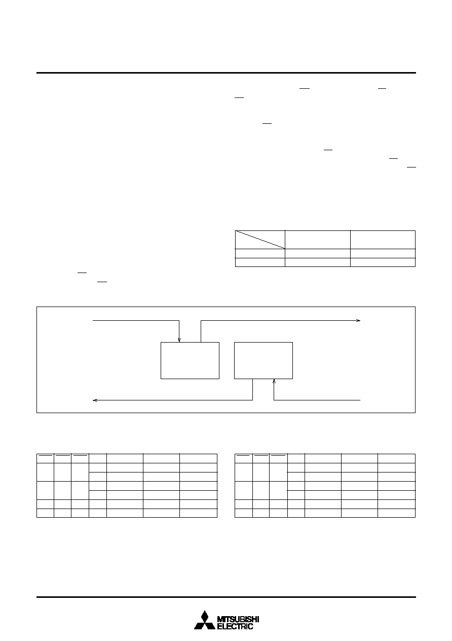
In this case, the same address is not selected when the same read/
write instruction is being executed at both ports as given in (1) and
(4). There is no concern about uncertainty of read/write data at an
active address. If one port operates in the write mode and the other
does in the read mode as given in (2) and (3), however, the same
address may be selected. In this case, data of the port operating in
the write mode is written. If the port in the read mode comes first,
read data of the first-in port becomes uncertain until write data of the
last-in port is determined (If the same address is selected, data of
the port operating in the write mode is written into memory. Therefore,
data of the port in the read mode may change from previously written
data to newly written ones during the same cycle) (See Fig 2).
Ex.) A port - address setting first-in read operation
A port address
B port address
WEB
B port I/O
(D
IN
)
A port I/O
(D
OUT
)
: When selecting the same address
Data B
Data B
Data A
(Data read to A port)
B port - address setting last-in write operation
Fig 2 Example of Read Data Transition at Selection of Same Address
(Data written from B port)

MITSUBISHI
DIGITAL ASSP
M66222SP/FP
128
×
8-BIT
×
2 MAIL-BOX
4
ABSOLUTE MAXIMUM RATINGS
(Ta = 0 ~ 70
°
C, unless otherwise noted)
Symbol
V
CC
V
I
V
O
P
d
T
stg
Parameter
Supply voltage
Input voltage
Output voltage
Maximum power dissipation
Storage temperature range
Conditions
When defining GND pin as a
reference.
Ta = 25
°
C
Ratings
0.3 ~ +7.0
0.3 ~ V
CC
+ 0.3
0 ~ V
CC
700
65 ~ 150
Unit
V
V
V
mW
°
C
RECOMMENDED OPERATING CONDITIONS
Symbol
V
CC
GND
V
I
T
opr
Parameter
Supply voltage
Ground
Input voltage
Operating temperature range
Unit
V
V
V
°
C
Limits
Min.
4.5
0
0
Typ.
5.0
0
Max.
5.5
V
CC
70
ELECTRICAL CHARACTERISTICS
(Ta = 0 ~ 70
°
C, Vcc=5V
±
10%, unless otherwise noted)
Test conditions
I
OH
= 2mA
I
OL
= 4mA
V
I
= V
CC
V
I
= GND
CS = V
IH
or OE = V
IH
V
O
= V
CC
CS = V
IH
or OE = V
IH
V
O
= GND
CS
<
0.2V,
Another input V
IN
>
V
CC
0.2V
or V
IN
<
0.2V, Output pin open
CSA, CSB = V
IH
CSA or CSB = V
IH
I
OUT
= 0mA
(Active port output pin open)
CSA, CSB
>
V
CC
0.2V
Another input V
IN
>
V
CC
0.2V
or V
IN
<
0.2V
CSA or CSB
>
V
CC
0.2V
Another input V
IN
>
V
CC
0.2V
or V
IN
<
0.2V, I
OUT
= 0mA
(Active port output pin open)
Symbol
V
IH
V
IL
V
OH
V
OL
I
IH
I
IL
I
OZH
I
OZL
I
CC
I
SB1
I
SB2
I
SB3
I
SB4
C
I
C
O
Parameter
"H" input voltage
"L" input voltage
"H" output voltage
"L" output voltage
"H" input current
"L" input current
Off state "H" output current
Off state "L" output current
Static current dissipation (active)
Two-port stand-by
One-port stand-by
Two-port full stand-by
One-port full stand-by
Input capacitance
Output capacitance in off state
Stand-by current
Unit
V
V
V
V
µ
A
µ
A
µ
A
µ
A
mA
mA
mA
mA
mA
pF
pF
Limits
Min.
2.2
0.3
2.4
Typ.
Max.
V
CC
+0.3
0.8
0.5
10.0
10.0
10.0
10.0
60
5
60
0.1
30
10
15
Notes 3: The direction in which current flows into the IC is defined as positive (no sign).
4: The above typical values are standard values for V
CC
=5V and T
a
=25
°
C.

MITSUBISHI
DIGITAL ASSP
M66222SP/FP
128
×
8-BIT
×
2 MAIL-BOX
5
SWITCHING CHARACTERISTICS
(Ta = 0 ~ 70
°
C, V
CC
= 5V
±
10%, unless otherwise noted)
Read cycle
Symbol
t
CR
t
a(A)
t
a(CS)
t
a(OE)
t
dis(CS)
t
dis(OE)
t
en(CS)
t
en(OE)
t
v(A)
Parameter
Read cycle time
Address access time
Chip select access time
Output enable access time
Output disable time after CS (Note 5)
Output disable time after OE (Note 5)
Output enable time after CS (Note 5)
Output enable time after OE (Note 5)
Data effective time after Address
Limits
Unit
ns
ns
ns
ns
ns
ns
ns
ns
ns
Typ.
Max.
70
70
35
35
35
Min.
70
5
5
10
TIMING REQUIREMENTS
(Ta = 0 ~ 70
°
C, V
CC
= 5V
±
10%, unless otherwise noted)
Write cycle
Parameter
Write cycle time
Write pulse width
Address setup time (for WE)
Address setup time (for CS)
Address setup time for rise of WE
Chip select setup time
Data setup time
Data hold time
Write recovery time
Output disable time after WE (Note 5)
Output disable time after OE (Note 5)
Output enable time after WE (Note 5)
Output enable time after OE (Note 5)
Limits
Unit
ns
ns
ns
ns
ns
ns
ns
ns
ns
ns
ns
ns
ns
Typ.
Max.
35
35
Min.
70
45
0
0
65
65
40
0
0
0
5
Note 5: The time required for the output to change from a steady state to
±
500mV under the load conditions shown in Figure 4.
This parameter is guaranteed but is not tested at shipment.
Symbol
t
CW
t
w(WE)
t
su(A)1
t
su(A)2
t
su(A-WEH)
t
su(CS)
t
su(D)
t
h(D)
t
rec(WE)
t
dis(WE)
t
dis(OE)
t
en(WE)
t
en(OE)