Supply voltage range·····Vcc=6 ~ 9V Rated supply voltage······Vcc=8V
V
DD
=4 ~ 6V V
DD
=5V
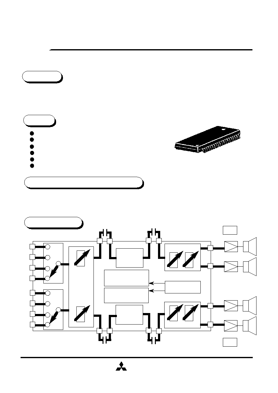
Block Diagram
ELECTRIC
MITSUBISHI
M62440FP
ELECTRIC VOLUME CONTROL WITH TONE
CONTROLLER FOR 4-SPEAKER APPLICATIONS
MITSUBISHI SOUND PROCESSOR
The M62440FP is an IC developed for car audio, it has a built-in 4ch input selector,
master volume, loudness, tone control and fader volume blocks. All of these blocks are
controlled via serial data.Thank to the used zero crossing detector, very low click noise
are obtained.
Outline 42P2R
(1/10)
Built-in zero cross detector prevents click noise
4-input Selector
Loudness
Tone Control Bass/Mid/Treble
Master Volume/Fader Volume
Serial Data Control
PRELIMINARY
Notice ; This is not a final specification.
some parametric limits are subject to change.
Bass/
Mid/
Treble
Fader
Fader
Interface
Lch
Front
Rear
Front
Rear
Rch
Zero Cross
Detector
Volume
&
Loudness
INC1
INB1
INA1
IND1
INC2
INB2
INA2
IND2
Description
Features
Recommended Operating Conditions
Bass/
Mid/
Treble
Zero Cross
Detector
MITSUBISHI
ELECTRIC
(2/10)
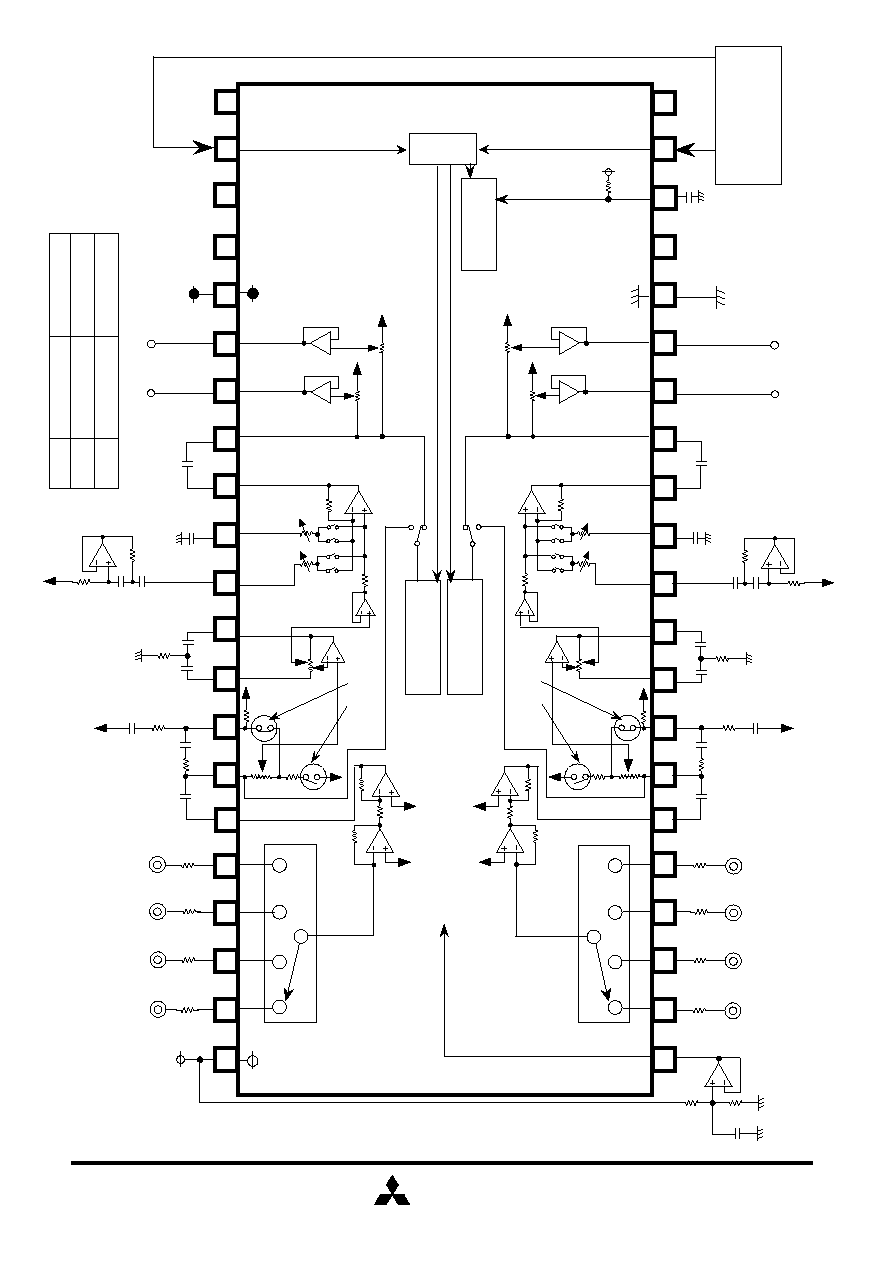
Pin Configuration & Application Example
SW A
SW B
Loudness ON
OFF
ON
Loudness OFF
ON
OFF
I/F
VDD
VDD
MCU
Vcc
200K
0.22
µ
16
17
18
9
12
13
14
10
11
15
7
8
1
3
5
4
33
31
30
36
35
27
29
28
32
34
38
39
40
42
FROUT
RROUT
1
µ
0.01
µ
FROUT
RROUT
VCC
VCC
ZERO CROSS
DETECTOR
0.068
µ
0.068
µ
6.8K
ZERO CROSS
DETECTOR
REF
22K
TIMER
DETECTOR
+
+
22K
+
+
1
µ
0.01
µ
0.068
µ
0.068
µ
6.8K
25
26
10
µ
47K
47K
6
37
19
24
GND
Loudness SW
Loudness SW
2.2
µ
2.2
µ
A
A
B
B
2
41
20
21
23
22
1.5K
100K
0.0033
µ
0.047
µ
1.5K
100K
0.0033
µ
0.047
µ
N.C.
N.C.
N.C.
INA1
INB1
INC1
IND1
INA2
INB2
INC3
IND4
N.C.
N.C.
22K
22K
22K
22K
22K
22K
22K
22K

MITSUBISHI
ELECTRIC
(3/10)
REF
INB1
IND1
1
2
3
5
TIM1
VOL IN1
BASSA1
6
7
8
9
MID1
TRE1
TONE OUT1
FADER IN1
GND
10
11
12
13
14
15
16
17
INA1
BASSB1
REAR OUT1
FRONT OUT1
Ground
DATA
LOUD IN1
19
20
SELECT OUT1
INC1
4
18
N.C.
Non Connection
N.C.
21
Pin Description
Pin No.
Symbol
Function
IC signal ground. Apply 1/2 Vcc
Input pin for channel 1 of the input
selector switch block
Output pin of the input selector switch block
Input pin of the volume block
Pin for setting the frequency characteristics
of the loudness block
Pin for setting the frequency characteristics
of the tone(Bass) block
R-ladder terminal of tone(Treble)
R-ladder terminal of tone(Mid)
Output pin of the tone block
Input pin of the fader volume
Output pin of the fader volume(Rear)
Output pin of the fader volume(Front)
Timer setting terminal
The relationship between outside parts
C and setting time is T=13.8X 10 ·C(sec).
Input pin of the control data
This pin inputs data in synchronization with CLOCK
Non Connection
4

MITSUBISHI
ELECTRIC
(4/10)
CLOCK
V
DD
IND2
24
26
27
28
VOL IN2
BASSB2
29
30
31
32
MID2
TRE2
TONE OUT2
FADER IN2
33
34
35
36
38
39
40
42
INB2
BASSA2
REAR OUT2
FRONT OUT2
Vcc
Digital power supply pin, normally +5V
INC2
Analog power supply pin
N.C.
23
37
LOUD IN2
22
N.C.
25
N.C.
INA2
41
SELECT OUT2
Non Connection
Input pin for channel 2 of the input
selector switch block
Output pin of the input selector switch block
Input pin of the volume block
Pin for setting the frequency characteristics
of the loudness block
Pin for setting the frequency characteristics
of the tone(Bass) block
R-ladder terminal of tone(Treble)
R-ladder terminal of tone(Mid)
Output pin of the tone block
Input pin of the fader volume
Output pin of the fader volume(Rear)
Output pin of the fader volume(Front)
Non Connection
Non Connection
Pin No.
Symbol
Function
Clock input pin for serial data transfer

Absolute Maximum Ratings
MITSUBISHI
ELECTRIC
(5/10)
Ratings
Vcc,V
DD
Supply Voltage
10 , 7
V
Pd
990
mW
Ta
25
K
9.9
mW/°C
Ta
25
T
opr
-30 ~ 85
-55 ~ 125
T
stg
25
50
75
100
125
150
200
400
600
800
1000
Thermal Derating
990
Ambient Temperature Ta [ °C ]
Power Dissipation Pd [ mW ]
Power Dissipation
Operating Temperature
Storage Temperature
85
°C
°C
Unit
Symbol
Parameter
Conditions
Thermal Derating Ratio