MITSUBISHI ELECTRIC
M5M5V416BUG - 70H I
revision-01, 17th July '00
4194304-BIT (262144-WORD BY 16-BIT) CMOS STATIC RAM
MITSUBISHI LSIs
* "ty pical" parameter is sampled, not 100% tested.
2.7 ~ 3.6V
0.3µA
1µA
3µA
1µA
15µA
30µA
50mA
(10MHz)
7mA
(1MHz)
70ns
M5M5V416BUG -70HI
Version,
Operating
temperature
I-
v ersion
-40 ~ +85°C
Part name
Power
Supply
Access time
max.
Stand-by c urrent Icc
(PD)
, Vcc=3.0V
ty pical *
Ratings (max.)
Activ e
current
(3.0V, ty p.)
Icc1
70°C
85°C
25°C
25°C
40°C
40°C
1
DESCRIPTION
The M5M5V416B is a f amily of low v oltage 4-Mbit static RAMs
organized as 262,144-words by 16-bit, f abricated by Mitsubishi's
high-perf ormance 0.25µm CMOS technology .
The M5M5V416B is suitable f or memory applications where a
simple interf acing , battery operating and battery backup are the
important design objectiv es.
M5M5V416BUG is packaged in a CSP (chip scale package),
with the outline of 7mm x 8.5mm, ball matrix of 6 x 8 (48pin) and
ball pitch of 0.75mm. It giv es the best solution f or a compaction
of mounting area as well as f lexibility of wiring pattern of printed
circuit boards.
Single +2.7~+3.6V power supply
Small stand-by current: 0.3µA(3V,ty p.)
No clocks, No ref resh
Data retention supply v oltage =2.0V to 3.6V
All inputs and outputs are TTL compatible.
Easy memory expansion by S1, S2, BC1 and BC2
Common Data I/O
Three-state outputs: OR-tie capability
OE prev ents data contention in the I/O bus
Process technology : 0.25µm CMOS
Package: 48pin 7mm x 8.5mm CSP
FEATURES
PIN CONFIGURATION
A0 ~ A17
DQ1 ~ DQ16
S1
W
OE
BC1
Address input
Data input / output
Chip select input 1
Write control input
Output enable input
Lower By te (DQ1 ~ 8)
Pin
Function
Vcc
GND
Power supply
Ground supply
BC2
Upper By te (DQ9 ~ 16)
S2
Chip select input 2
(TOP VIEW)
Outline:
48FJA
NC: No Connection
1
2
3
4
5
6
A
B
C
D
E
F
G
DQ3
A7
DQ1
S2
VCC
GND
DQ7
A2
S1
DQ2
DQ4
DQ5
DQ6
A1
A4
A6
A5
A17
A16
A15
A0
A3
GND
A14
OE
BC2
DQ11
DQ12
DQ13
DQ14
BC1
DQ9
DQ10
GND
VCC
DQ15
DQ8
W
A13
A12
N.C.
DQ16
N.C.
A11
A10
A9
A8
N.C.
H
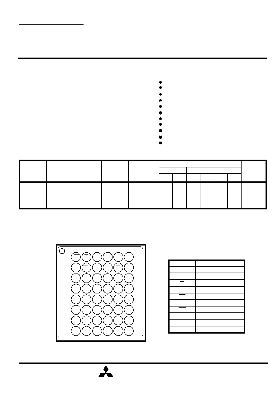
Those are summarized in the part name table below.

MITSUBISHI ELECTRIC
M5M5V416BUG - 70H I
revision-01, 17th July '00
4194304-BIT (262144-WORD BY 16-BIT) CMOS STATIC RAM
MITSUBISHI LSIs
2
FUNCTION
The M5M5V416BWG is organized as 262,144-words by
16-bit. These dev ices operate on a single +2.7~3.6V power
supply , and are directly TTL compatible to both input and
output. Its f ully s t atic circuit needs no clocks and no
ref resh, and makes it usef ul.
The operation mode are determined by a combination of
the dev ice control inputs BC1 , BC2 , S1, S2 , W and OE.
Each mode is summarized in the f unction table.
A write operation is executed whenev er the low lev el W
ov erlaps with the low lev el BC1 and/or BC2 and the low
lev el S1 and the high lev el S2. The address(A0~A17) must
be set up bef ore the write cy cle and must be stable during
the entire cycle.
A read operation is executed by s etting W at a high lev el
and OE at a low lev el while BC1 and/or BC2 and S1 and
S2 are in an activ e state(S1=L,S2=H).
When setting BC1 at the high lev el and other pins are in
an activ e stage , upper-by t e are in a selectable mode in
which both reading and writing are enabled, and lower-by t e
are in a non-selectable mode. And when setting BC2 at a
high lev el and other pins are in an activ e stage, lower-
by t e are in a selectable mode and upper-by te are in a
non-selectable mode.
When setting BC1 and BC2 at a high lev el or S1 at a high
lev el or S2 at a low lev el, the chips are in a non-selectable
mode in which both reading and writing are disabled. In this
mode, the output stage is in a high-impedance state, allowing
OR-tie with other chips and memory expansion by BC1, BC2
and S1, S2.
The power supply c urrent is reduced as low as 0.3µA(25°C,
ty pical), and the memory data can be held at +2V power
supply , enabling battery back-up operation during power
f ailure or power-down operation in the non-selected mode.
BLOCK DIAGRAM
MEMORY ARRAY
262144 WORDS
x 16 BITS
CLOCK
GENERATOR
A
0
A
1
A
16
A
17
S2
BC1
BC2
W
OE
DQ
8
DQ
1
DQ
16
DQ
9
-
Vcc
GND
S1
FUNCTION TABLE
Mode
S2
W
BC1 BC2
OE
DQ1~8
DQ9~16
Icc
High-Z High-Z
H
X
L
L
H
Din
High-Z
Activ e
H
H
L
H
Read
High-Z
Dout
Activ e
L
H
H
L
Activ e
H
H
L
Activ e
H
L
High-Z
High-Z
Activ e
H
L
H
H
High-Z
H
L
Dout
H
L
L
Read
Dout
Activ e
H
L
Din
L
L
X
Write
Din
Activ e
H
High-Z
H
H
High-Z High-Z
Non selection
X
H
H
X
X
Standby
Write
H
H
L
L
Write
Din
Activ e
X
H
L
H
Read
High-Z
Activ e
L
Dout
H
High-Z
S1
L
L
L
L
L
L
L
X
L
L
L
X
X
High-Z
X
X
Non selection
High-Z Standby
X
X
High-Z
X
X
Non selection
High-Z Standby
H
X
X
MITSUBISHI ELECTRIC
M5M5V416BUG - 70H I
revision-01, 17th July '00
4194304-BIT (262144-WORD BY 16-BIT) CMOS STATIC RAM
MITSUBISHI LSIs
3
ABSOLUTE MAXIMUM RATINGS
pF
10
V
I
=GND, V
I
=25mVrms, f =1MHz
V
O
=
GND,V
O
=25mVrms, f =1MHz
C
I
C
O
Symbol
Parameter
Limits
Conditions
Units
µA
mA
µA
mA
V
Icc
1
Icc
2
Icc
4
V
IH
V
IL
I
O
Icc
3
V
OH1
I
OH
= -0.5mA
V
OH2
I
OH
= -0.05mA
V
OL
I
OL
=2mA
I
I
V
I
=0
~
Vcc
BC1 and BC2=VIH or S1=VIH or S2=VIH or OE=VIH, VI/O=0 ~ Vcc
Vcc+0.3V
0.6
2.2
-0.3 *
2.4
0.5
0.4
±1
70
50
20
Vcc-0.5V
±1
15
Max
Ty p
Min
DC ELECTRICAL CHARACTERISTICS
+70°C
+40°C
0.3
f = 10MHz
f = 1MHz
-
-
-
-
-
-
-
-
Supply v oltage
Input v oltage
Output v oltage
Power dissipation
Operating
temperature
Storage temperature
V
mW
Conditions
Ta=25°C
700
- 65 ~ +150
Ratings
Vcc
V
I
V
O
P
d
T
a
T
stg
-0.5
*
~ +4.6
-0.5
*
~ Vcc + 0.5
0 ~ Vcc
Symbol
Parameter
Units
- 40 ~ +85
I-v ersion
With respect to GND
f = 10MHz
f = 1MHz
7
70
50
15
7
+85°C
- 20 ~ +25°C
- 40 ~ +25°C
0 ~ +25°C
-
-
-
0.3
0.3
1
2.0
5.0
-
-
40
-
With respect to GND
With respect to GND
( Vcc=2.7 ~ 3.6V, unless otherwise noted)
High-lev el input v oltage
Low-lev el input v oltage
High-level output voltage 1
High-level output voltage 2
Low-lev el output v oltage
Input leakage current
Output leakage current
Activ e supply c urrent
( AC,MOS lev el )
( AC,TTL lev el )
Activ e supply c urrent
Stand by s upply current
( AC,MOS lev el )
( AC,TTL lev el )
Stand by s upply current
Other inputs= 0 ~ Vcc
* -3.0V in case of AC (Pulse width 30ns)
Note 1: Direction for current flowing into IC is indicated as positive (no mark)
Note 2: Typical value is for Vcc=3.0V and Ta=25
°
C
CAPACITANCE
(Vcc=2.7 ~ 3.6V, unless otherwise noted)
Symbol
Parameter
Conditions
Limits
Max
Ty p
Min
Units
Input capacitance
Output capacitance
* -3.0V in case of AC (Pulse width 30ns)
BC1 and BC2 0.2V, S1 0.2V, S2 Vcc-0.2V
other inputs 0.2V or Vcc-0.2V
Output - open (duty 100%)
<
=
<
=
>
=
BC1 and BC2=V
IL
, S=V
IL
,S2=V
IH
<
=
other pins =V
IH or
V
IL
Output - open (duty 100%)
Other inputs=0~Vcc
S1 Vcc - 0.2V,
other inputs = 0 ~ Vcc
>
=
>
=
S1 0.2V, S2 Vcc - 0.2V
<
=
< 1 >
< 3 >
BC1 and BC2 Vcc - 0.2V
BC1 and BC2=V
IH
or S1=V
IH
or S2=V
IL
2.0
2.0
<
=
<
=
10
°C
°C
S2 0.2V,
other inputs = 0 ~ Vcc
< 2 >
>
=

MITSUBISHI ELECTRIC
M5M5V416BUG - 70H I
revision-01, 17th July '00
4194304-BIT (262144-WORD BY 16-BIT) CMOS STATIC RAM
MITSUBISHI LSIs
AC ELECTRICAL CHARACTERISTICS
(Vcc=2.7 ~ 3.6V, unless otherwise noted)
Input rise time and f all time
Ref erence lev el
Output loads
2.7V~3.6V
V
IH
=2.4V,V
IL
=0.4V
V
OH
=V
OL
=1.5V
Transition is measured ±500mV f rom
steady state voltage.(f or t
en
,t
dis
)
5ns
Fig.1,CL=30pF
CL=5pF (for ten,tdis)
(1) TEST CONDITIONS
Supply v oltage
Input pulse
1TTL
CL
DQ
Fig.1 Output load
Including scope and
jig capacitance
4
(2) READ CYCLE
(3) WRITE CYCLE
t
CR
ns
t
a
(S1)
t
a
(OE)
t
dis
(S1)
t
dis
(OE)
t
en
(S1)
t
en
(OE)
t
V
(A)
t
a
(A)
ns
ns
ns
ns
ns
ns
ns
ns
t
a
(BC1)
t
a
(BC2)
t
dis
(BC1)
t
dis
(BC2)
t
en
(BC1)
t
en
(BC2)
ns
ns
ns
ns
ns
ns
t
a
(S2)
ns
t
en
(S2)
ns
t
dis
(S2)
ns
70
10
10
10
10
10
35
70
70
70
70
25
25
25
25
70
25
Symbol
Parameter
Read cy cle time
Limits
Address access time
Chip select 1 access time
Chip select 2 access time
By te control 1 access time
By te control 2 access time
Output enable access time
Output disable time af t er S2 low
Output disable time af t er S1 high
Output disable time af t er BC1 high
Max
Min
Units
Output disable time af t er BC2 high
Output disable time af t er OE high
Output enable time af ter S1 low
Output enable time af ter S2 high
Output enable time af ter BC1 low
Output enable time af ter BC2 low
Output enable time af ter OE low
Data v alid time after address
5
t
su
(A-WH)
t
CW
t
w
(W)
t
su
(A)
t
su
(S1)
t
su
(D)
t
h
(D)
t
rec
(W)
t
dis
(W)
t
dis
(OE)
t
en
(W)
t
en
(OE)
ns
70
ns
ns
ns
ns
ns
ns
ns
ns
ns
ns
ns
ns
ns
55
0
60
25
25
5
5
t
su
(BC1)
t
su
(BC2)
60
60
60
35
0
0
t
su
(S2)
ns
60
Max
Min
Limits
Units
Write cy cle time
Write pulse width
Address setup time
Address setup time with respect to W
By te control 1 setup time
By te control 2 setup time
Chip select 1 setup time
Chip select 2 setup time
Data setup time
Data hold time
Write recov ery time
Output disable time f rom W low
Output disable time f rom OE high
Output enable time f rom W high
Output enable time f rom OE low
Symbol
Parameter
MITSUBISHI ELECTRIC
M5M5V416BUG - 70H I
revision-01, 17th July '00
4194304-BIT (262144-WORD BY 16-BIT) CMOS STATIC RAM
MITSUBISHI LSIs
S2
(Note3)
(Note3)
t
su
(S2)
t
en
(W)
5
t
a
(A)
t
a
(BC1)
t
v
(A)
t
dis
(BC1) or
t
dis
(BC1)
t
a
(OE)
t
en
(OE)
t
dis
(OE)
t
CR
t
h
(D)
t
su
(D)
DQ
1~16
t
su
(BC1) or
t
su
(BC2)
t
en
(OE)
t
dis
(OE)
t
w
(W)
t
rec
(W)
t
su
(A)
t
dis
(W)
t
CW
t
en
(S1)
W = "H" lev el
A
0~17
DQ
1~16
A
0~17
OE
OE
W
(4)TIMING DIAGRAMS
Read cycle
(Note3)
(Note3)
(Note3)
(Note3)
VALID DATA
Write cycle ( W control mode )
DATA IN
STABLE
(Note3)
(Note3)
t
a
(S1)
t
dis
(S1)
S1
(Note3)
(Note3)
BC1 ,BC2
t
a
(BC2)
or
t
en
(BC2)
t
en
(BC1)
t
su
(A-WH)
S1
(Note3)
(Note3)
t
su
(S1)
BC1,BC2
t
a
(S2)
t
dis
(S2)
S2
(Note3)
(Note3)
t
en
(S2)