
MITSUBISHI LSIs
16,777,216-BIT (1048,576-WORD BY16-BIT)
CMOS 3.3V-ONLY, BLOCK ERASE FLASH MEMORY
M5M29GB/T161BWG
Sep.1999. Rev4.0
1
DESCRIPTION
The MITSUBISHI Mobile FLASH M5M29GB/T161BWG are 3.3V-only high speed 16,777,216-bit CMOS boot block Flash Memories with
alternating BGO (Back Ground Operation) feature. The BGO feature of the device allows Program or Erase operations to be performed in
one bank while the device simultaneously allows Read operations to be performed on the other bank. This BGO feature is suitable for
mobile and personal computing, and communication products. The M5M29GB/T161BWG are fabricated by CMOS technology for the
peripheral circuits and DINOR(Divided bit line NOR) architecture for the memory cells, and are available in 6x8-balls CSP (0.75mm ball
pitch) .
FEATURES
PIN CONFIGURATION (TOP VIEW)
APPLICATION
Digital Cellular Phone
Telecommunication
Mobile Computing Machine
PDA (Personal Digital Assistance)
Car Navigation System
Video Game Machine
Boot Block
M5M29GB161BWG Bottom Boot
M5M29GT161BWG Top Boot
Other Functions
Soft Ware Command Control
Selective Block Lock
Erase Suspend/Resume
Program Suspend/Resume
Status Register Read
Alternating Back Ground Program/Erase Operation
Between Bank(I) and Bank(II)
Package
7mm x 8.5mm CSP (Chip Scale Package)
- 6 x 8 balls, 0.75mm ball pitch
........................
........................
NC : NO CONNECTION
INDEX
M5M29GB/T161BWG
A13
A11
A14
A15
A12
A10
WE#
A8
A9
A16
NC
GND
D15
D7
D5
D6
D13
WP2#
RP#
WP1#
A18
D11
D12
D4
VCC
D3
D2
D10
D1
OE#
D0
GND
D8
CE#
A0
A1
A3
A6
A2
A5
A17
A4
A7
D14
D9
NC
NC
8.5mm
7.0mm
A
B
C
D
E
F
G
H
6
5
4
3
2
1
CSP(0.75mm ball pitch):48FJA
16-bit version
A19
Organization 1048,576 word x 16bit
(M5M29GB/T161BWG)
Supply voltage
................................
V
CC
= 2.7~3.6V
Access time 90ns (Max.)
Power Dissipation
Read 54 mW (Max. at 5MHz)
(After Automatic Power saving) 0.33
�
W (typ.)
Program/Erase 126 mW (Max.)
Standby 0.33
�
W (typ.)
Deep power down mode 0.33
�
W (typ.)
Auto program for Bank(I)
Program Time 4ms (typ.)
Program Unit
(Byte Program) 1word
(Page Program) 128word
Auto program for Bank(II)
Program Time 4ms (typ.)
Program Unit 128word
Auto Erase
Erase time 40 ms (typ.)
Erase Unit
Bank(I) Boot Block 16Kword x 1
Parameter Block 16Kword x 7
Bank(II) Main Block 32Kword x 28
Program/Erase cycles 100Kcycles
.................................
.................................
.............................
.......................
..............................
.................................
.....................
..............
......................
.........................................
.................................
.........................
.........................
.................................
.................................
.................................
..........
.......................
MITSUBISHI LSIs
16,777,216-BIT (1048,576-WORD BY16-BIT)
CMOS 3.3V-ONLY, BLOCK ERASE FLASH MEMORY
M5M29GB/T161BWG
Sep.1999. Rev4.0
2
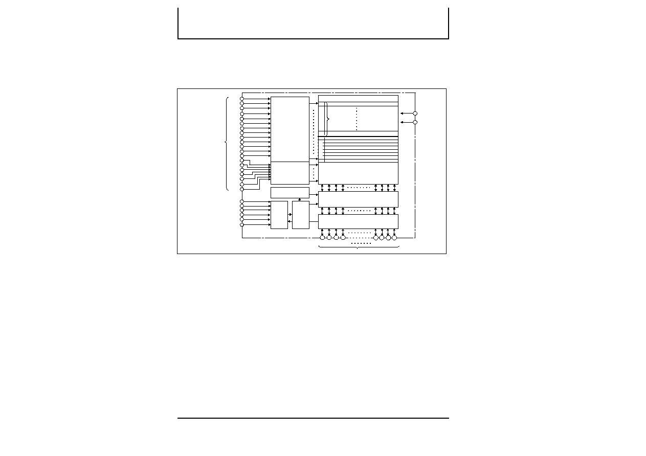
M5M29GB/T161BWG (16 bit version)
BLOCK DIAGRAM
X-DECODER
Y-DECODER
Y-GATE / SENSE AMP.
INPUT/OUTPUT
BUFFERS
CE#
OE#
WE#
V
CC
(3.3V)
GND (0V)
DATA INPUTS/OUTPUTS
DQ
15
DQ
14
DQ
13
DQ
12
DQ
2
DQ
1
DQ
0
DQ
3
WP1#
RP#
MULTIPLEXER
CUI
WSM
STATUS / ID REGISTER
128 WORD PAGE BUFFER
Main Block 32KW
A
18
A
17
A
16
A
15
A
14
A
13
A
12
A
11
A
10
A
9
A
8
A
7
A
6
A
5
A
4
A
3
A
2
A
1
A
0
ADDRESS
INPUTS
CHIP ENABLE INPUT
OUTPUT ENABLE INPUT
WRITE ENABLE INPUT
WRITE PROTECT INPUT
RESET/POWER DOWN INPUT
Main Block 32KW
Bank(II)
28
WP2#
WRITE PROTECT INPUT
Parameter Block5 16KW
Parameter Block6 16KW
Boot Block 16KW
Parameter Block3 16KW
Parameter Block4 16KW
Parameter Block1 16KW
Parameter Block2 16KW
Bank(I)
Parameter Block7 16KW
A
19

MITSUBISHI LSIs
16,777,216-BIT (1048,576-WORD BY16-BIT)
CMOS 3.3V-ONLY, BLOCK ERASE FLASH MEMORY
M5M29GB/T161BWG
Sep.1999. Rev4.0
FUNCTION
Deep Power-Down
When RP# is at VIL, the device is in the deep powerdown
mode and its power consumption is substantially low. During
read modes, the memory is deselected and the data
input/output are in a high-impedance(High-Z) state. After
return from powerdown, the CUI is reset to Read Array , and
the Status Register is cleared to value 80H.
During block erase or program modes, RP# low will abort
either operation. Memory array data of the block being altered
become invalid.
The M5M29GB/T161BWG includes on-chip program/erase control
circuitry. The Write State Machine (WSM) controls block erase
and byte/page program operations. Operational modes are
selected by the commands written to the Command User Interface
(CUI). The Status Register indicates the status of the WSM and
when the WSM successfully completes the desired program or
block erase operation.
A Deep Powerdown mode is enabled when the RP# pin is at GND,
minimizing power consumption.
Read
The M5M29GB/T161BWG has three read modes, which accesses
to the memory array, the Device Identifier and the Status Register.
The appropriate read command are required to be written to the
CUI. Upon initial device powerup or after exit from deep
powerdown, the M5M29GB/T161BWG automatically resets to read
array mode. In the read array mode, low level input to CE# and
OE#, high level input to WE# and RP#, and address signals to the
address inputs (A19-A0:M5M29GB/T161BWG) output the data of
the addressed location to the data input/output
(D15-D0:M5M29GB/T161BWG).
Write
Writes to the CUI enables reading of memory array data, device
identifiers and reading and clearing of the Status Register. They
also enable block erase and program. The CUI is written by
bringing WE# to low level, while CE# is at low level and OE# is at
high level. Address and data are latched on the earlier rising edge
of WE# and CE#. Standard micro-processor write timings are
used.
Standby
When CE# is at VIH, the device is in the standby mode and its
power consumption is reduced. Data input/output are in a
high-impedance(High-Z) state. If the memory is deselected
during block erase or program, the internal control circuits
remain active and the device consume normal active power
until the operation completes.
Alternating Background Operation (BGO)
The M5M29GB/T161BWG allows to read array from one bank
while the other bank operates in software command write cycling
or the erasing / programming operation in the background. Read
array operation with the other bank in BGO is performed by
changing the bank address without any additional command.
When the bank address points the bank in software command
write cycling or the erasing / programming operation, the data is
read out from the status register. The access time with BGO is the
same as the normal read operation.
Output Disable
When OE# is at VIH, output from the devices is disabled. Data
input/output are in a high-impedance(High-Z) state.
Automatic Power-Saving (APS)
The Automatic Power-Saving minimizes the power
consumption during read mode. The device automatically
turns to this mode when any addresses or CE# isn't changed
more than 200ns after the last alternation. The power
consumption becomes the same as the stand-by mode. While
in this mode, the output data is latched and can be read out.
New data is read out correctly when addresses are changed.
3

MITSUBISHI LSIs
16,777,216-BIT (1048,576-WORD BY16-BIT)
CMOS 3.3V-ONLY, BLOCK ERASE FLASH MEMORY
M5M29GB/T161BWG
Sep.1999. Rev4.0
SOFTWARE COMMAND DEFINITIONS
The device operations are selected by writing specific software
command into the Command User Interface.
Read Array Command (FFH)
The device is in Read Array mode on initial device power up and
after exit from deep powerdown, or by writing FFH to the
Command User Interface. After starting the internal operation the
device is set to the read status register mode automatically.
Read Device Identifier Command (90H)
It can normally read device identifier codes when Read Device
Identifier Code Command(90H) is written to the command latch.
Following the command write, the manufacturer code and the
device code can be read from address 0000H and 0001H,
respectively.
Read Status Register Command (70H)
The Status Register is read after writing the Read Status Register
command of 70H to the Command User Interface. Also, after
starting the internal operation the device is set to the Read Status
Register mode automatically.
The contents of Status Register are latched on the later falling
edge of OE# or CE#. So CE# or OE# must be toggled every status
read.
Clear Status Register Command (50H)
The Erase Status, Program Status and Block Status bits are set to
"1"s by the Write State Machine and can only be reset by the Clear
Status Register command of 50H. These bits indicates various
failure conditions.
Block Erase / Confirm Command (20H/D0H)
Automated block erase is initiated by writing the Block Erase
command of 20H followed by the Confirm command of D0H. An
address within the block to be erased is required. The WSM
executes iterative erase pulse application and erase verify
operation.
Program Commands
A)Word Program (40H)
Word program is executed by a two-command sequence. The
Word Program Setup command of 40H is written to the
Command Interface, followed by a second write specifying the
address and data to be written. The WSM controls the program
pulse application and verify operation. The Word Program
Command is Valid for only Bank(I).
DATA PROTECTION
The M5M29GB/T161BWG provides selectable block locking of
memory blocks. Each block has an associated nonvolatile lock-bit
which determines the lock status of the block. In addition, the
M5M29GB/T161BWG have a master Write Protect pin (WP1# &
WP2#) which prevents any modifications to memory blocks whose
lock-bits are set to "0", when WP1# or WP2# is low. When WP1#
& WP2# are high , all blocks can be programmed or erased
regardless of the state of the lock-bits, and the lock-bits are
cleared to "1" by erase. See the BLOCK LOCKING table on P.9 for
details.
Power Supply Voltage
When the power supply voltage (Vcc) is less than V
LKO,
Low V
CC
Lock-Out voltage, the device is set to the Read-only mode.
Regarding DC electrical characteristics of V
LKO,
see P.9
A delay time of 2 us is required before any device operation is
initiated. The delay time is measured from the time Vcc reaches
Vccmin (2.7V).
During power up, RP#=GND is recommended. Falling in Busy
status is not recommended for possibility of damaging the device.
MEMORY ORGANIZATION
The M5M29GB/T161BWG has one 16Kword boot block, seven
16Kword parameter blocks, for Bank(I) and twenty-eight 32Kword
main blocks for Bank(II). A block is erased independently of other
blocks in the array.
Suspend/Resume Command (B0H/D0H)
Writing the Suspend command of B0H during block erase
operation interrupts the block erase operation and allows read out
from another block of memory. Writing the Suspend command of
B0H during program operation interrupts the program operation
and allows read out from another block of memory. The Bank
address is required when writing the Suspend/Resume Command.
The device continues to output Status Register data when read,
after the Suspend command is written to it. Polling the WSM
Status and Suspend Status bits will determine when the erase
operation or program operation has been suspended. At this
point, writing of the Read Array command to the CUI enables
reading data from blocks other than that which is suspended.
When the Resume command of D0H is written to the CUI,
the WSM will continue with the erase or program processes.
4
B)Page Program for Data Blocks (41H)
Page Program for Bank(I) and Bank(II) allows fast programming of
128words of data. Writing of 41H initiates the page program
operation for the Data area. From 2nd cycle to 129th cycle , write
data must be serially inputted. Address A6-A0 have to be
incremented from 00H to 7FH. After completion of data loading, the
WSM controls the program pulse application and verify operation.
C)Single Data Load to Page Buffer (74H)
/ Page Buffer to Flash (0EH/D0H)
Single data load to the page buffer is performed by writing 74H
followed by a second write specifying the column address and
data. Distinct data up to 128word can be loaded to the page
buffer by this two-command sequence. On the other hand, all of
the loaded data to the page buffer is programed simultaneously
by writing Page Buffer to Flash command of 0EH followed by the
confirm command of D0H. After completion of programing the
data on the page buffer is cleared automatically.
This command is valid for only Bank(I) alike Word Program.
Clear Page Buffer Command (55H)
Loaded data to the page buffer is cleared by writing the Clear
Page Buffer command of 55H followed by the Confirm command
of D0H. This command is valid for clearing data loaded by Single
Data Load to Page Buffer command.
MITSUBISHI LSIs
16,777,216-BIT (1048,576-WORD BY16-BIT)
CMOS 3.3V-ONLY, BLOCK ERASE FLASH MEMORY
M5M29GB/T161BWG
Sep.1999. Rev4.0
M 5 M 29G T 160B WG
Operating Voltage :
29G : 2.7 - 3.6V
Standard / BGO Type
29W : 1.65 - 2.2V
Standard / BGO Type
Boot Block :
T : Top Boot
B : Bottom Boot
Package :
VP : 48pin TSOP(I) 12mm x 20mm (Nomal Pinout)
WG: CSP Ball Pitch 0.75mm,6x8 array, 7mm x 8.5mm
Density/Write Protect/
Word Organizetion:
Mitsubishi 16M Flash Memory Type name
5
160B : 16M WP1#, x8/x16
161B : 16M WP1# & WP2#, x16
MITSUBISHI LSIs
16,777,216-BIT (1048,576-WORD BY16-BIT)
CMOS 3.3V-ONLY, BLOCK ERASE FLASH MEMORY
M5M29GB/T161BWG
Sep.1999. Rev4.0
6
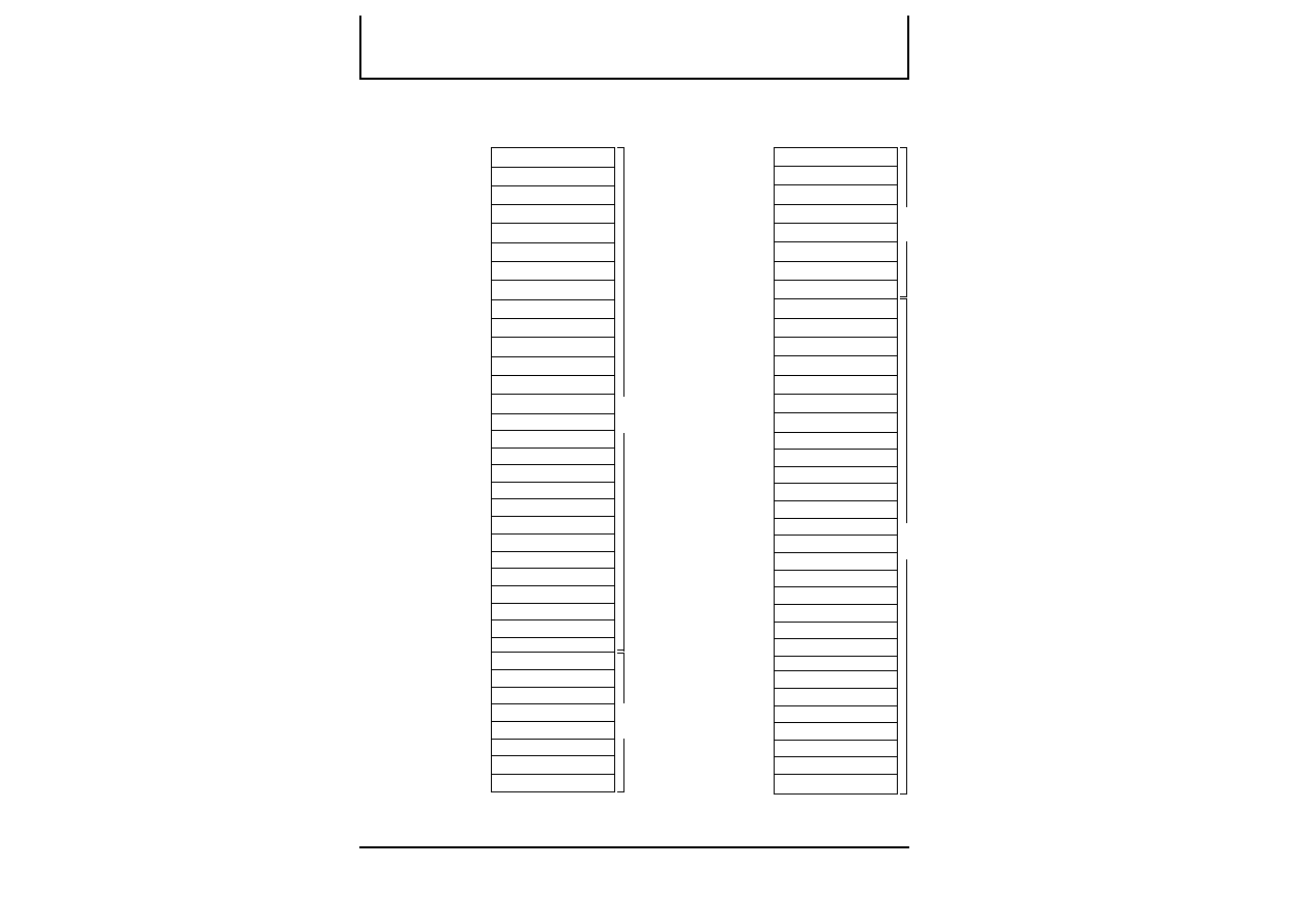
M5M29GT161BWG Memory Map
BANK(I)
BANK(II)
16Kword BOOT BLOCK 35
16Kword PARAMETER BLOCK 34
32Kword MAIN BLOCK 27
32Kword MAIN BLOCK 26
32Kword MAIN BLOCK 25
32Kword MAIN BLOCK 24
32Kword MAIN BLOCK 23
32Kword MAIN BLOCK 22
32Kword MAIN BLOCK 21
32Kword MAIN BLOCK 20
32Kword MAIN BLOCK 19
32Kword MAIN BLOCK 18
32Kword MAIN BLOCK 17
32Kword MAIN BLOCK 16
32Kword MAIN BLOCK 15
32Kword MAIN BLOCK 14
32Kword MAIN BLOCK 13
32Kword MAIN BLOCK 12
32Kword MAIN BLOCK 11
32Kword MAIN BLOCK 10
32Kword MAIN BLOCK 9
32Kword MAIN BLOCK 8
32Kword MAIN BLOCK 7
32Kword MAIN BLOCK 6
32Kword MAIN BLOCK 5
32Kword MAIN BLOCK 4
32Kword MAIN BLOCK 3
32Kword MAIN BLOCK 2
32Kword MAIN BLOCK 1
32Kword MAIN BLOCK 0
16Kword PARAMETER BLOCK 33
16Kword PARAMETER BLOCK 32
16Kword PARAMETER BLOCK 31
16Kword PARAMETER BLOCK 30
16Kword PARAMETER BLOCK 29
16Kword PARAMETER BLOCK 28
MEMORY ORGANIZATION
A
19
-A
0
(M5M29GB161BWG)
M5M29GB161BWG Memory Map
32Kword MAIN BLOCK 35
32Kword MAIN BLOCK 34
32Kword MAIN BLOCK 33
32Kword MAIN BLOCK 32
32Kword MAIN BLOCK 31
32Kword MAIN BLOCK 30
32Kword MAIN BLOCK 29
32Kword MAIN BLOCK 28
32Kword MAIN BLOCK 27
32Kword MAIN BLOCK 26
32Kword MAIN BLOCK 25
32Kword MAIN BLOCK 24
32Kword MAIN BLOCK 23
32Kword MAIN BLOCK 22
BANK(II)
32Kword MAIN BLOCK 21
32Kword MAIN BLOCK 20
32Kword MAIN BLOCK 19
32Kword MAIN BLOCK 18
32Kword MAIN BLOCK 17
32Kword MAIN BLOCK 16
32Kword MAIN BLOCK 15
32Kword MAIN BLOCK 14
32Kword MAIN BLOCK 13
32Kword MAIN BLOCK 12
32Kword MAIN BLOCK 11
32Kword MAIN BLOCK 10
32Kword MAIN BLOCK 9
32Kword MAIN BLOCK 8
BANK(I)
16Kword PARAMETER BLOCK 1
16Kword BOOT BLOCK 0
16Kword PARAMETER BLOCK 2
16Kword PARAMETER BLOCK 3
16Kword PARAMETER BLOCK 4
16Kword PARAMETER BLOCK 5
16Kword PARAMETER BLOCK 6
16Kword PARAMETER BLOCK 7
x16 ( Wordmode)
F8000H-FFFFFH
F0000H-F7FFFH
E8000H-EFFFFH
E0000H-E7FFFH
D8000H-DFFFFH
D0000H-D7FFFH
C8000H-CFFFFH
C0000H-C7FFFH
B8000H-BFFFFH
B0000H-B7FFFH
A8000H-AFFFFH
A0000H-A7FFFH
98000H-9FFFFH
90000H-97FFFH
00000H-03FFFH
18000H-1BFFFH
14000H-17FFFH
10000H-13FFFH
0C000H-0FFFFH
08000H-0BFFFH
04000H-07FFFH
1C000H-1FFFFH
20000H-27FFFH
28000H-2FFFFH
30000H-37FFFH
38000H-3FFFFH
40000H-47FFFH
48000H-4FFFFH
50000H-57FFFH
58000H-5FFFFH
60000H-67FFFH
68000H-6FFFFH
70000H-77FFFH
78000H-7FFFFH
80000H-87FFFH
88000H-8FFFFH
x16 ( Wordmode)
FC000H-FFFFFH
F8000H-FBFFFH
F4000H-F7FFFH
F0000H-F3FFFH
EC000H-EFFFFH
E8000H-EBFFFH
E4000H-E7FFFH
E0000H-E3FFFH
D8000H-DFFFFH
D0000H-D7FFFH
C8000H-CFFFFH
C0000H-C7FFFH
B8000H-BFFFFH
B0000H-B7FFFH
00000H-07FFFH
30000H-37FFFH
28000H-2FFFFH
20000H-27FFFH
18000H-1FFFFH
10000H-17FFFH
08000H-0FFFFH
38000H-3FFFFH
40000H-47FFFH
48000H-4FFFFH
50000H-57FFFH
58000H-5FFFFH
60000H-67FFFH
68000H-6FFFFH
70000H-77FFFH
78000H-7FFFFH
80000H-87FFFH
88000H-8FFFFH
90000H-97FFFH
98000H-9FFFFH
A0000H-A7FFFH
A8000H-AFFFFH
A
19
-A
0
(M5M29GT161BWG)

MITSUBISHI LSIs
16,777,216-BIT (1048,576-WORD BY16-BIT)
CMOS 3.3V-ONLY, BLOCK ERASE FLASH MEMORY
M5M29GB/T161BWG
Sep.1999. Rev4.0
7
1) X can be V
IH
or V
IL
for control pins.
BUS OPERATIONS
Bus Operations for Word-Wide Mode (
M5M29GB/T161BWG
)
Mode
Array
Status Register
Identifier Code
Stand by
Program
Erase
Write
Read
Pins
CE#
OE#
WE#
V
IL
V
IL
V
IL
V
IL
V
IH
V
IL
V
IL
V
IL
V
IL
V
IL
V
IH
X
V
IH
V
IH
V
IH
V
IH
V
IH
V
IH
X
V
IL
V
IL
Data out
Status Register Data
Identifier Code
Hi-Z
Hi-Z
Command/Data in
Command
Output disable
Deep Power Down
Others
RP#
V
IH
V
IH
V
IH
V
IH
V
IH
V
IH
V
IH
X
V
IL
V
IH
X
V
IL
X
Hi-Z
V
IH
V
IL
Command
DQ
0-15
1)
V
IH
Lock Bit Status
V
IL
V
IL
V
IH
Lock Bit Data (DQ
6
)

MITSUBISHI LSIs
16,777,216-BIT (1048,576-WORD BY16-BIT)
CMOS 3.3V-ONLY, BLOCK ERASE FLASH MEMORY
M5M29GB/T161BWG
Sep.1999. Rev4.0
SOFTWARE COMMAND DEFINITION
Command List
1) Upper byte data (DQ8-DQ15) is ignored.
2) IA=ID Code Address : A0=VIL (Manufacturer's Code) : A0=VIH (Device Code), ID=ID Code
3) Bank = Bank Address (Bank(I) or Bank(II)). A19-A17.
4) SRD = Status Register Data
5) Word Program, Single Data Load and Page Buffer to Flash Command is valid for only Bank(I).
6) WA = Write Address,WD = Write Data
7) WA0,WAn=Write Address, WD0,WDn=Write Data.
: Write Address and Write Data must be provided sequentially from 00H to 7FH for A6-A0. Page size is 128word (128word x 16bit).
and also A19-A7(Block Address, Page Address) must be valid.
8) WA = Write Address : Upper page address, A19-A7(Block Address, Page Address) must be valid.
9) BA = Block Address : Bank1: A19-A14
Bank2: A19-A15
10) DQ6 provides Block Lock Status, DQ6 = 1 : Block Unlock, DQ6 = 0 : Block Locked.
8
Read Array
FFH
X
Write
1st bus cycle
2nd bus cycle
Command
Device Identifier
90H
X
Write
ID
IA
Read
Read Status Register
70H
Write
SRD
Read
Clear Status Register
50H
X
Write
2)
4)
2)
Page Program
Write
41H
Block Erase / Confirm
Suspend
Resume
7)
Read Lock Bit Status
Lock Bit Program / Confirm
Erase All Unlocked Blocks
Write
Write
20H
Bank
Write
D0H
Write
B0H
Bank
Write
71H
X
Write
9)
Write
Write
A7H
77H
D0H
Write
Read
BA
X
D0H
D0H
DQ6
Word Program
5)
Write
40H
Write
WD0
Write
7)
7)
WD
10)
Single Data Load to Page Buffer
Page Buffer to Flash
Write
Write
74H
Write
WD
WA
0EH
Write
D0H
3)
Clear Page Buffer
55H
X
Write
Write
X
D0H
5)
5)
Bank
Bank
Bank(I)
WA
Bank
Bank
BA
Bank
X
WDn
Write
7)
7)
WAn
WA0
3rd ~129th bus cycles (
M5M29GB/T161BWG
)
1)
1)
Address
Mode
Data
Address
Mode
Data
Address
Mode
Data
1)
(DQ15-0)
1)
1)
1)
WA
6)
8)
6)
(DQ15-0)
(DQ15-0)
BA
5)
Bank(I)
5)
Bank(I)
5)

MITSUBISHI LSIs
16,777,216-BIT (1048,576-WORD BY16-BIT)
CMOS 3.3V-ONLY, BLOCK ERASE FLASH MEMORY
M5M29GB/T161BWG
Sep.1999. Rev4.0
9
BLOCK LOCKING
1) DQ
6
provides Lock Status of each block after writing the Read Lock Status command (71H).
WP1# & WP2# pins must not be switched during performing Erase / Write operations or WSM Busy (WSMS = 0).
2) Erase/Write command for locked blocks is aborted. At this time read mode is not array read mode but status read mode and
00B0H is read. Please issue Clear Status Register command plus Read Array command to change the mode from status read mode
to array read mode.
STATUS REGISTER
Status
Erase Status
Program Status
Definition
Symbol
(DQ
5
)
(DQ
4
)
Write State Machine Status
(DQ
7
)
(DQ
6
)
(DQ
1
)
(DQ
0
)
(DQ
3
)
(DQ
2
)
"1"
"0"
Ready
Busy
Suspended
Operation in Progress / Completed
Error
Successful
Error
Successful
SR.5
SR.4
SR.7
SR.6
SR.1
SR.0
SR.3
SR.2
Block Status after Program
Reserved
-
Suspend Status
Error
Successful
-
*DQ3 indicates the block status after the page programming, byte/word programming and page buffer to flash. When DQ3 is "1", the page has the
over-programed cell . If over-program occurs, the device is block fail. However if DQ3 is "1", please try the block erase to the block. The block may revive.
Reserved
Reserved
-
-
-
-
Deep Power Down Mode
Write Protection Provided
Locked
V
IL
RP#
WP1#
WP2#
X
X
Lock
Bit
(Internally)
X
BANK(I)
Lock Bit
Boot
Parameter
Data
Locked
Locked
Locked
Note
All Blocks Locked
All Blocks Unlocked
V
IH
V
IL
V
IH
V
IH
V
IL
V
IL
V
IL
V
IH
V
IH
0
1
X
X
0
1
Locked
Locked
Unlocked
Locked
Locked
Locked
Locked
Locked
Locked
Locked
Locked
Locked
Unlocked Unlocked Unlocked
Locked
Locked
Locked
Unlocked Unlocked
Locked
Unlocked
Locked
Locked
Only Parameter Block is Unlocked
BANK(II)
161BWG
MITSUBISHI LSIs
16,777,216-BIT (1048,576-WORD BY16-BIT)
CMOS 3.3V-ONLY, BLOCK ERASE FLASH MEMORY
M5M29GB/T161BWG
Sep.1999. Rev4.0
10
CAPACITANCE
Symbol
Parameter
Test conditions
pF
pF
Unit
Max
8
12
Typ
Min
Limits
Ta = 25
�
C, f = 1MHz, V
in
= V
out
= 0V
Input capacitance (Address, Control Pins)
Output capacitance
C
IN
C
OUT
1) Minimum DC voltage is -0.5V on input/output pins. During transitions, this level may undershoot to -2.0V for periods <20ns. Maximum DC voltage
on input/output pins is V
CC
+0.5V which, during transitions, may overshoot to V
CC
+1.5V for periods <20ns.
ABSOLUTE MAXIMUM RATINGS
Conditions
Parameter
With respect to Ground
Symbol
V
cc
All input or output voltage except V
cc,
A9,RP#
V
I1
V
cc
voltage
1)
Unit
V
V
Min
Max
4.6
-0.2
Ambient temperature
Temperature under bias
T
a
T
bs
Storage temperature
T
stg
�
C
�
C
�
C
85
-50
95
-65
125
Output short circuit current
I
OUT
mA
100
-0.6
4.6
-40
All currents are in RMS unless otherwise noted.
1) Typical values at Vcc=3.3V, Ta=25
�
C
2) To protect against initiation of write cycle during Vcc power-up/ down, a write cycle is locked out for Vcc less than V
LKO.
If Vcc is less than V
LKO, Write State Machine is reset to read mode. When the Write State Machine is in Busy state, if Vcc is less than V
LKO
, the alteration of memory contents
may occur.
DEVICE IDENTIFIER CODE
The upper data(D
15-8)
is "0".
Code
Manufacturer Code
Pins
Hex. Data
1CH
DQ
0
0
A
0
V
IL
DQ
1
0
DQ
2
1
DQ
3
1
DQ
4
1
DQ
5
DQ
6
0
DQ
7
0
Device Code (-T161BWG)
A0H
V
IH
0
0
1
Device Code (-B161BWG)
V
IH
1
0
0
1
1
0
0
0
0
0
0
0
A1H
0
1
DC ELECTRICAL CHARACTERISTICS
(Ta = -40~ 85
�
C, Vcc = 2.7V ~ 3.6V, unless otherwise noted)
Symbol
Parameter
Max
Typ1)
Limits
Min
Test conditions
Unit
V
CC
standby current
I
LO
�
10
Output leakage current
�
A
0V
V
OUT
V
CC
I
LI
Input leakage current
�
A
0V
V
IN
V
CC
�
1.0
V
CC
deep powerdown current
I
CC3
V
CC
program current
mA
35
V
CC
= 3.6V, V
IN
=V
IL
/V
IH
, CE# = RP# =WP# = V
IH
I
CC4
V
CC
erase current
mA
35
V
CC
= 3.6V, V
IN
=V
IL
/V
IH
, CE# = RP# =WP# = V
IH
Output high voltage
V
V
OL
Output low voltage
V
I
OL
= 4.0mA
0.45
Vcc+0.5
V
IH
Input high voltage
V
2.0
0.8
V
IL
Input low voltage
� 0.5
V
OH1
I
OH
= �2.0mA
0.85Vcc
V
V
OH2
I
OH
= �100
�
A
Vcc�0.4
V
V
LKO
Low V
CC
Lock-Out voltage 2)
1.5
2.2
V
I
CC5
V
CC
suspend current
200
V
CC
= 3.6V, V
IN
=V
IL
/V
IH
, CE# = RP# =WP# = V
IH
�
A
I
SB2
5
V
CC
= 3.6V, V
IN
=GND or V
CC
,
CE# = RP# = WP# = V
CC
�
0.3V
�
A
0.1
15
mA
I
CC1
V
CC
read current for Word or Byte
V
CC
= 3.6V, V
IN
=V
IL
/V
IH
, CE# = V
IL
,
RP#=OE#=V
IH
, I
OUT
= 0mA
8
I
SB1
V
CC
= 3.6V, V
IN
=V
IL
/V
IH
, CE# = RP# =WP# = V
IH
�
A
200
50
I
CC2
15
mA
V
CC
Write current for Word or Byte
V
CC
= 3.6V,V
IN
=V
IL
/V
IH
, CE# =WE#= V
IL
,
RP#=OE#=V
IH
V
CC
= 3.6V, V
IN
=V
IL
/V
IH
, RP# = V
IL
�
A
15
5
I
SB3
�
A
0.1
I
SB4
V
CC
= 3.6V, V
IN
=GND or V
CC
, RP# =GND
�
0.3V
5
5MHz
4
2
1MHz

MITSUBISHI LSIs
16,777,216-BIT (1048,576-WORD BY16-BIT)
CMOS 3.3V-ONLY, BLOCK ERASE FLASH MEMORY
M5M29GB/T161BWG
Sep.1999. Rev4.0
11
Read-Only Mode
AC ELECTRICAL CHARACTERISTICS
(Ta = -40 ~85
�
C, Vcc = 2.7V ~3.6V)
Write Mode (WE# control)
AC ELECTRICAL CHARACTERISTICS
(Ta = -40 ~85
�
C, Vcc = 2.7V ~3.6V)
Timing measurements are made under AC waveforms for read operations.
Symbol
Parameter
Limits
t
a (AD)
Address access time
t
AVQV
t
CLZ
Chip enable to output in low-Z
t
ELQX
t
a (CE)
Chip enable access time
t
ELQV
t
a (OE)
Output enable access time
t
GLQV
t
DF(CE)
Chip enable high to output in high Z
t
EHQZ
t
RC
Read cycle time
t
AVAV
t
OH
Output hold from CE#, OE#, addresses
t
OH
t
OLZ
t
GLQX
Output enable to output in low-Z
t
DF(OE)
t
GHQZ
Output enable high to output in high Z
t
PHZ
RP# low to output high-Z
t
PLQZ
RP# recovery to CE# low
Unit
ns
ns
ns
ns
ns
ns
ns
ns
ns
ns
ns
t
PS
t
PHEL
Vcc=2.7-3.6V
90
0
90
30
25
90
0
0
25
150
150
Max
Min
Typ
90ns
Read timing parameters during command write operations mode are the same as during read-only operations mode.
Typical values at Vcc=3.3V, Ta=25
�
C
Symbol
Parameter
Write cycle time
Data hold time
Data set-up time
Address hold time
Address set-up time
t
AVAV
t
WHDX
t
DVWH
t
WHAX
t
AVWH
t
WC
t
DH
t
DS
t
AH
t
AS
Limits
90ns
90
50
50
Max
Min
Typ
0
0
Unit
ns
ns
ns
ns
ns
Write pulse width
Chip enable hold time
Chip enable set-up time
Write pulse width high
RP# high recovery to write enable low
Block Lockhold from valid SRD
Write enable high to F-RY/BY# low
Duration of auto-program operation
Duration of auto-block erase operation
Block Lock set-up to write enable high
t
WLWH
t
WHEH
t
ELWL
t
WHWL
t
PHWL
t
QVPH
t
WHRL
t
WHRH1
t
WHRH2
t
PHHWH
t
WHRL
t
WP
t
CH
t
CS
t
WPH
t
PS
t
BLS
t
BLH
t
DAP
t
DAE
OE# hold to WE# Low
t
GHWL
t
GHWL
150
4
40
90
80
600
60
0
30
0
90
0
0
ns
ns
ns
ns
ns
ns
ns
ms
ms
ns
ns
Vcc=2.7-3.6V
ns
ns
10
30
OE# hold from WE# high
t
WHGL
t
OEH
-
t
RE
Latency between Read and Write FFH or 71H

MITSUBISHI LSIs
16,777,216-BIT (1048,576-WORD BY16-BIT)
CMOS 3.3V-ONLY, BLOCK ERASE FLASH MEMORY
M5M29GB/T161BWG
Sep.1999. Rev4.0
12
Erase and Program Performance
Block Erase Time
Main Block Write Time (Page Mode)
Page Write Time
Parameter
ms
sec
ms
Unit
Typ
4
1.0
40
Max
80
1.8
600
Min
Vcc Power Up / Down Timing
Symbol
Unit
Typ
2
Max
Min
t
VCS
Parameter
RP# =V
IH
set-up time from Vccmin
�
s
During power up/down, by the noise pulses on control pins, the device has possibility of accidental erasure or programming.
The device must be protected against initiation of write cycle for memory contents during power up/down.
The delay time of min.2
�
sec is always required before read operation or write operation is initiated from the time Vcc reaches Vccmin during power up/down.
By holding RP# VIL, the contents of memory is protected during Vcc power up/down.
During power up, RP# must be held VIL for min.2
�
s from the time Vcc reaches Vccmin.
During power down, RP# must be held VIL until Vcc reaches GND.
RP# doesn't have latch mode ,therefore RP# must be held VIH during read operation or erase/program operation.
Program Suspend Latency / Erase Suspend Time
Program Suspend Latency
Erase Suspend Time
Parameter
Unit
Typ
Max
15
15
Min
�
s
�
s
Please see page 19.
Please see page 12.
Write Mode (F-CE# control)
AC ELECTRICAL CHARACTERISTICS
(Ta = -40 ~ 85
�
C, Vcc = 2.7V ~ 3.6V)
Read timing parameters during command write operation mode are the same as during read-only operation mode.
Typical values at Vcc=3.3V, Ta=25
�
C
Symbol
Parameter
Write cycle time
Data hold time
Data set-up time
Address hold time
Address set-up time
t
AVAV
t
EHDX
t
DVWH
t
EHAX
t
AVWH
t
WC
t
DH
t
DS
t
AH
t
AS
Limits
90ns
90
50
50
Max
Min
Typ
0
0
Unit
ns
ns
ns
ns
ns
CE# pulse width
Write enable hold time
Write enable set-up time
CE# pulse width high
RP# high recovery to write enable low
Block Lockhold from valid SRD
CE# high to F-RY/BY# low
Duration of auto-program operation
Duration of auto-block erase operation
Block Lock set-up to chip enable high
t
ELEH
t
EHWH
t
WLEL
t
EHEL
t
PHWL
t
QVPH
t
EHRL
t
EHRH1
t
EHRH2
t
PHHEH
t
EHRL
t
CEP
t
WH
t
WS
t
CEPH
t
PS
t
BLS
t
BLH
t
DAP
t
DAE
OE# hold to CE# Low
t
GHEL
t
GHEL
150
4
40
90
80
600
60
0
30
0
90
0
90
ns
ns
ns
ns
ns
ns
ns
ms
ms
ns
ns
Vcc=2.7-3.6V
ns
ns
10
30
OE# hold from CE# high
t
EHGL
t
OEH
-
t
RE
Latency between Read and Write FFH or 71H
MITSUBISHI LSIs
16,777,216-BIT (1048,576-WORD BY16-BIT)
CMOS 3.3V-ONLY, BLOCK ERASE FLASH MEMORY
M5M29GB/T161BWG
Sep.1999. Rev4.0
13
3.3V
GND
V
CC
Vcc POWER UP / DOWN TIMING
V
IH
V
IL
RP#
Read /Write Inhibit
t
VCS
V
IH
V
IL
CE#
V
IH
V
IL
WE#
t
PS
t
PS
Read /Write Inhibit
Read /Write Inhibit
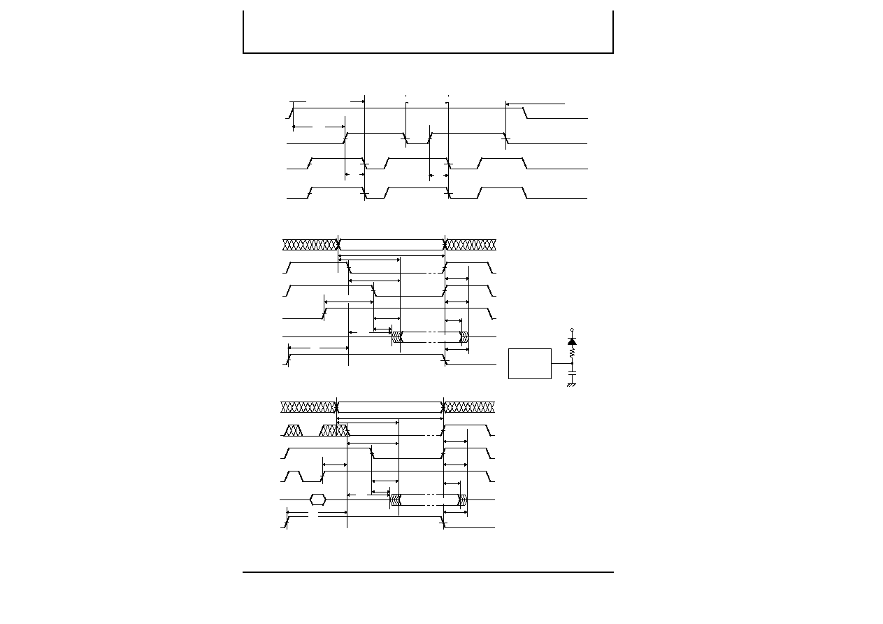
TEST CONDITIONS
FOR AC CHARACTERISTICS
Input voltage : V
IL
= 0V, V
IH
= 3.0V
Input rise and fall times :
5ns
Reference voltage
at timing measurement : 1.5V
Output load : 1TTL gate +CL(30pF)
or
DUT
3.3k
1N914
1.3V
C
L
AC WAVEFORMS FOR READ OPERATION AND TEST CONDITIONS
OUTPUT VALID
HIGH-Z
t
DF(OE)
t
RC
V
IH
V
IL
V
IH
V
IL
V
IH
V
IL
V
IH
V
IL
V
OH
V
OL
ADDRESSES
CE#
OE#
WE#
DATA
ADDRESS VALID
t
OH
t
OLZ
t
a (CE)
t
OEH
t
CLZ
t
a (AD)
t
a (OE)
HIGH-Z
V
IH
V
IL
RP#
t
PS
t
DF(CE)
t
PHZ
AC WAVEFORMS FOR WRITE FFH or 71H AND READ OPERATION
OUTPUT VALID
HIGH-Z
t
DF(OE)
t
RC
V
IH
V
IL
V
IH
V
IL
V
IH
V
IL
V
IH
V
IL
V
OH
V
OL
ADDRESSES
CE#
OE#
WE#
DATA
ADDRESS VALID
t
OH
t
OLZ
t
a (CE)
t
RE
t
CLZ
t
a (AD)
t
a (OE)
HIGH-Z
V
IH
V
IL
RP#
t
PS
t
DF(CE)
t
PHZ
Valid
FFH or 71H
In the case of use CE# is Low fixed, it is allowed to define a timming specification of tRE
from rising edge of WE# to falling edge of OE#, and valid data is read after spec of tRE+ta(CE).
(This is only for FFH,71H program and read)

MITSUBISHI LSIs
16,777,216-BIT (1048,576-WORD BY16-BIT)
CMOS 3.3V-ONLY, BLOCK ERASE FLASH MEMORY
M5M29GB/T161BWG
Sep.1999. Rev4.0
14
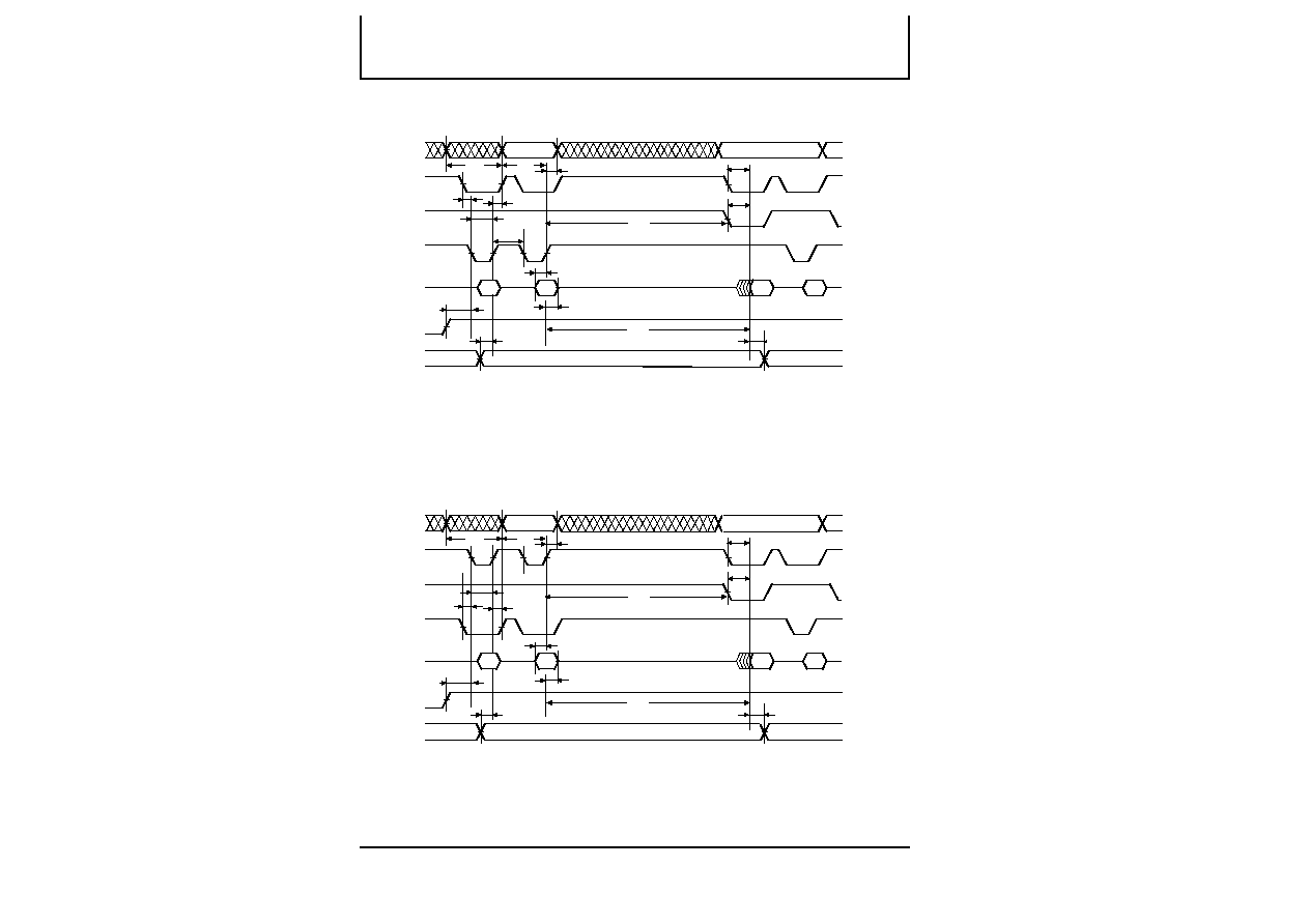
AC WAVEFORMS FOR PAGE PROGRAM OPERATION (WE# control)
AC WAVEFORMS FOR PAGE PROGRAM OPERATION (CE# control)
41H
DIN
t
WPH
t
WP
t
DS
t
DH
t
CS
t
CH
t
WC
V
IH
V
IL
V
IH
V
IL
V
IH
V
IL
V
IH
V
IL
ADDRESS VALID
CE#
OE#
WE#
DATA
t
AH
V
IH
V
IL
t
AS
DIN
SRD
DIN
V
IH
V
IL
t
OEH
t
DAP
PROGRAM
READ STATUS
REGISTER
WRITE READ
ARRAY COMMAND
FFH
7FH
01H~7EH
00H
t
a(CE)
t
a(OE)
V
IL
V
IH
V
IL
WP1#,
WP2#
t
BLH
t
BLS
t
PS
V
IH
RP#
BANK ADDRESS VALID
The other bank
address
VALID
VALID
DOUT
t
OEH
t
GHWL
t
a(OE)
t
a(CE)
VALID
A6~A0
A19~A7
DIN
t
CEPH
t
CEP
t
DS
t
DH
t
WS
t
WH
t
WC
V
IH
V
IL
V
IH
V
IL
V
IH
V
IL
V
IH
V
IL
ADDRESS VALID
CE#
OE#
WE#
DATA
t
AH
V
IH
V
IL
t
AS
DIN
SRD
DIN
V
IH
V
IL
t
OEH
t
DAP
PROGRAM
READ STATUS
REGISTER
WRITE READ
ARRAY COMMAND
FFH
7FH
01H~7EH
00H
t
a(CE)
t
a(OE)
BANK ADDRESS VALID
VALID
VALID
VALID
DOUT
t
a(CE)
t
OEH
t
GHEL
t
a(OE)
The other bank
address
A6~A0
A19~A7
t
PS
V
IH
V
IL
RP#
V
IH
V
IL
t
BLH
WP1#,
WP2#
t
BLS
41H
MITSUBISHI LSIs
16,777,216-BIT (1048,576-WORD BY16-BIT)
CMOS 3.3V-ONLY, BLOCK ERASE FLASH MEMORY
M5M29GB/T161BWG
Sep.1999. Rev4.0
15
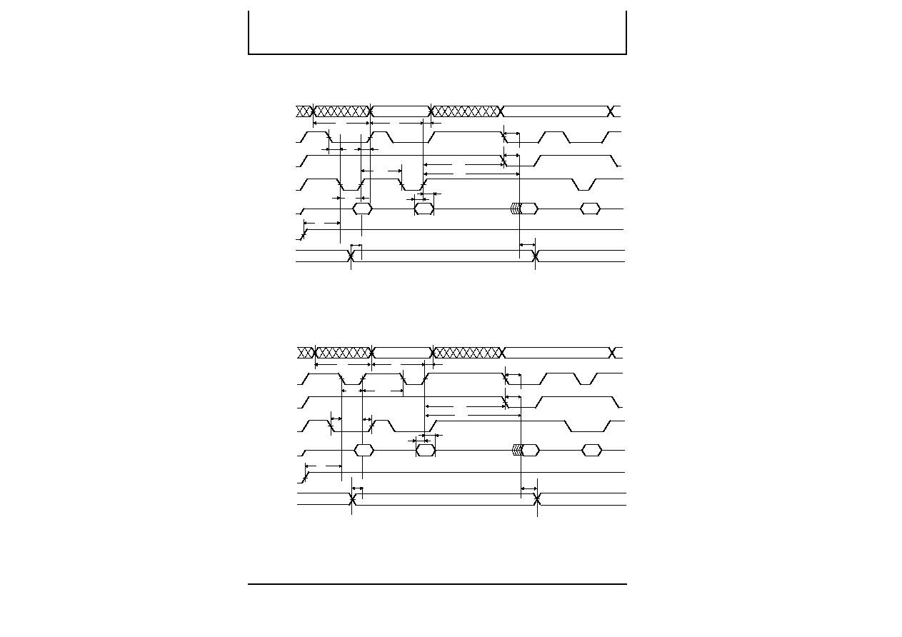
AC WAVEFORMS FOR BYTE / WORD PROGRAM OPERATION (CE# control) (to only BANK(I))
AC WAVEFORMS FOR BYTE / WORD PROGRAM OPERATION (WE# control) (to only BANK(I))
WRITE READ
ARRAY COMMAND
READ STATUS
REGISTER
V
IH
V
IL
ADDR
ADDRESS
VALID
PROGRAM
V
IH
V
IL
V
IH
V
IL
V
IH
CE#
OE#
WE#
DATA
V
IL
V
IH
V
IL
V
IH
V
IL
RST#
V
IH
V
IL
40H
DIN
t
CS
t
CH
t
WPH
t
WP
t
DS
t
PS
t
DAP
t
OEH
t
a(CE)
t
a(OE)
t
BLH
SRD
FFH
t
AH
t
AS
t
WC
t
BLS
BANK(I) ADDRESS VALID
WP1#,
WP2#
t
DH
WRITE READ
ARRAY COMMAND
READ STATUS
REGISTER
V
IH
V
IL
A
DDR
ADDRESS
VALID
PROGRAM
V
IH
V
IL
V
IH
V
IL
V
IH
CE#
OE#
WE#
DATA
V
IL
V
IH
V
IL
V
IH
V
IL
RP#
V
IH
V
IL
40H
DIN
t
WS
t
WH
t
CEP
t
DS
t
PS
t
DAP
t
OEH
t
a(CE)
t
a(OE)
t
BLH
t
DH
SRD
FFH
t
AH
t
AS
t
WC
t
BLS
BANK(I) ADDRESS VALID
WP1#,
WP2#
MITSUBISHI LSIs
16,777,216-BIT (1048,576-WORD BY16-BIT)
CMOS 3.3V-ONLY, BLOCK ERASE FLASH MEMORY
M5M29GB/T161BWG
Sep.1999. Rev4.0
16
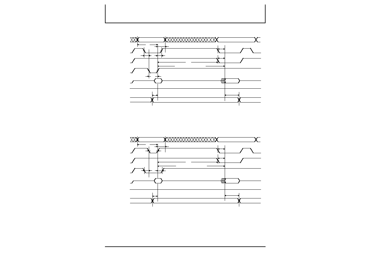
AC WAVEFORMS FOR ERASE OPERATIONS (WE# control)
AC WAVEFORMS FOR ERASE OPERATIONS (CE# control)
20H
D0H
t
WPH
t
WP
t
DS
t
DH
t
CS
t
CH
t
WC
V
IH
V
IL
V
IH
V
IL
V
IH
V
IL
V
IH
V
IL
t
AH
V
IH
V
IL
ADDRESSES
t
AS
FFH
SRD
t
OEH
t
DAE
ADDRESS VALID
ERASE
READ STATUS
REGISTER
WRITE READ
ARRAY COMMAND
CE#
OE#
WE#
DATA
t
a(OE)
t
a(CE)
BANK ADDRESS VALID
V
IL
V
IH
V
IL
t
PS
V
IH
RP#
t
BLS
t
BLH
WP1#,
WP2#
20H
D0H
t
CEPH
t
CEP
t
DS
t
DH
t
WS
t
WH
t
WC
V
IH
V
IL
V
IH
V
IL
V
IH
V
IL
V
IH
V
IL
t
AH
V
IH
V
IL
ADDRESSES
t
AS
FFH
SRD
t
OEH
t
DAE
ADDRESS VALID
ERASE
READ STATUS
REGISTER
WRITE READ
ARRAY COMMAND
CE#
OE#
WE#
DATA
t
a(OE)
t
a(CE)
BANK ADDRESS VALID
V
IL
V
IH
V
IL
t
PS
V
IH
RP#
t
BLH
t
BLS
WP1#,
WP2#

MITSUBISHI LSIs
16,777,216-BIT (1048,576-WORD BY16-BIT)
CMOS 3.3V-ONLY, BLOCK ERASE FLASH MEMORY
M5M29GB/T161BWG
Sep.1999. Rev4.0
17
AC WAVEFORMS FOR PAGE PROGRAM OPERATION WITH BGO (WE# control)
AC WAVEFORMS FOR PAGE PROGRAM OPERATION WITH BGO (CE# control)
ARRAY READ FROM THE OTHER BANK
WITH BGO
V
IH
V
IL
V
IH
V
IL
V
IH
V
IL
V
IH
ADDRESS VALID
CE#
OE#
WE#
DATA
V
IH
V
IL
V
IL
V
IH
V
IL
7FH
01H~7EH
00H
41H
DIN
DOUT
DIN
DIN
SRD
VALID
VALID
VALID
VALID
t
WC
t
AS
t
AH
t
CS
t
CH
t
WPH
t
WP
t
DS
t
DH
t
a(CE)
t
a(OE)
t
OEH
DOUT
PROGRAM DATA TO ONE BANK
Change Bank Address
A6~A0
A19~A7
~ ~
~ ~
~ ~
~ ~
~ ~
~ ~
ARRAY READ FROM THE OTHER BANK
WITH BGO
V
IH
V
IL
V
IH
V
IL
V
IH
V
IL
V
IH
ADDRESS VALID
CE#
OE#
WE#
DATA
V
IH
V
IL
V
IL
V
IH
V
IL
7FH
01H~7EH
00H
41H
DIN
DOUT
DIN
DIN
SRD
VALID
VALID
VALID
VALID
t
WC
t
AS
t
AH
t
WS
t
CH
t
CEPH
t
CEP
t
DS
t
DH
t
a(CE)
t
a(OE)
t
OEH
DOUT
PROGRAM DATA TO ONE BANK
Change Bank Address
A6~A0
A19~A7
~ ~
~ ~
~ ~
~ ~

MITSUBISHI LSIs
16,777,216-BIT (1048,576-WORD BY16-BIT)
CMOS 3.3V-ONLY, BLOCK ERASE FLASH MEMORY
M5M29GB/T161BWG
Sep.1999. Rev4.0
18
AC WAVEFORMS FOR BYTE / WORD PROGRAM OPERATION WITH BGO (WE# control)
ARRAY READ FROM BANK(II) WITH BGO
V
IH
V
IL
V
IH
V
IL
V
IH
V
IL
V
IH
ADDRESS VALID
CE#
OE#
WE#
DATA
V
IH
V
IL
V
IL
V
IH
V
IL
40H
DIN
DOUT
SRD
VALID
VALID
VALID
VALID
t
WC
t
AS
t
AH
t
CS
t
CH
t
WPH
t
WP
t
DS
t
DH
t
a(CE)
t
a(OE)
t
OEH
DOUT
PROGRAM DATA TO
BANK(I)
VALID
READ STATUS
REGISTER
Change Bank Address
A6~A0
A19~A7
AC WAVEFORMS FOR BYTE / WORD PROGRAM OPERATION WITH BGO (CE# control)
Change Bank Address
ARRAY READ FROM BANK(II) WITH BGO
V
IH
V
IL
V
IH
V
IL
V
IH
V
IL
V
IH
CE#
OE#
WE#
DATA
V
IH
V
IL
V
IL
V
IH
V
IL
40H
DIN
DOUT
SRD
VALID
VALID
VALID
VALID
t
WC
t
AS
t
WS
t
CH
t
CEPH
t
CEP
t
DS
t
DH
t
a(CE)
t
a(OE)
t
OEH
DOUT
PROGRAM DATA TO
BANK(I)
VALID
ADDRESS VALID
READ STATUS
REGISTER
A6~A0
A19~A7

MITSUBISHI LSIs
16,777,216-BIT (1048,576-WORD BY16-BIT)
CMOS 3.3V-ONLY, BLOCK ERASE FLASH MEMORY
M5M29GB/T161BWG
Sep.1999. Rev4.0
19
AC WAVEFORMS FOR BLOCK ERASE OPERATION WITH BGO (WE# control)
ARRAY READ FROM THE OTHER
BANK WITH BGO
V
IH
V
IL
V
IH
V
IL
V
IH
V
IL
V
IH
ADDRESSES
ADDRESS VALID
CE#
OE#
WE#
DATA
V
IL
V
IH
V
IL
20H
D0H
DOUT
SRD
VALID
VALID
t
WC
t
AS
t
AH
t
CS
t
CH
t
WPH
t
WP
t
DS
t
DH
t
a(CE)
t
a(OE)
t
OEH
DOUT
BLOCK ERASE IN
ONE BANK
READ STATUS
REGISTER
Change Bank Address
AC WAVEFORMS FOR BLOCK ERASE OPERATION WITH BGO (CE# control)
V
IH
V
IL
V
IH
V
IL
V
IH
V
IL
V
IH
CE#
OE#
WE#
DATA
V
IL
V
IH
V
IL
20H
D0H
DOUT
SRD
VALID
VALID
t
WC
t
AS
t
WS
t
CH
t
CEPH
t
CEP
t
DS
t
DH
t
a(CE)
t
a(OE)
t
OEH
DOUT
ADDRESS VALID
t
AH
READ DATA FROM THE OTHER BANK
WITH BGO
ADDRESSES
BLOCK ERASE IN
ONE BANK
READ STATUS
REGISTER
Change Bank Address
MITSUBISHI LSIs
16,777,216-BIT (1048,576-WORD BY16-BIT)
CMOS 3.3V-ONLY, BLOCK ERASE FLASH MEMORY
M5M29GB/T161BWG
Sep.1999. Rev4.0
20
AC WAVEFORMS FOR SUSPEND OPERATION (WE# control)
B0H
t
WP
t
CS
t
CH
V
IH
V
IL
V
IH
V
IL
V
IH
V
IL
V
IH
V
IL
V
IH
V
IL
ADDRESSES
t
AS
t
OEH
BANK ADDRESS VALID
READ STATUS
REGISTER
CE#
OE#
WE#
DATA
t
a(OE)
t
a(CE)
BANK ADDRESS VALID
V
IL
V
IH
V
IL
V
IH
RP#
t
BLS
t
BLH
t
AH
VALID SRD
Program Suspend Latency
WP1#,
WP2#
S.R.6,7=1
AC WAVEFORMS FOR SUSPEND OPERATION (CE# control)
B0H
V
IH
V
IL
V
IH
V
IL
V
IH
V
IL
V
IH
V
IL
V
IH
V
IL
ADDRESSES
t
AS
t
OEH
Program Suspend Latency
t
CEP
BANK ADDRESS VALID
READ STATUS
REGISTER
CE#
OE#
WE#
DATA
t
a(OE)
t
a(CE)
BANK ADDRESS VALID
V
IL
V
IH
V
IL
V
IH
RP#
t
BLS
VALID SRD
t
BLH
t
AH
t
WS
t
WH
WP1#,
WP2#
S.R.6,7=1

MITSUBISHI LSIs
16,777,216-BIT (1048,576-WORD BY16-BIT)
CMOS 3.3V-ONLY, BLOCK ERASE FLASH MEMORY
M5M29GB/T161BWG
Sep.1999. Rev4.0
21
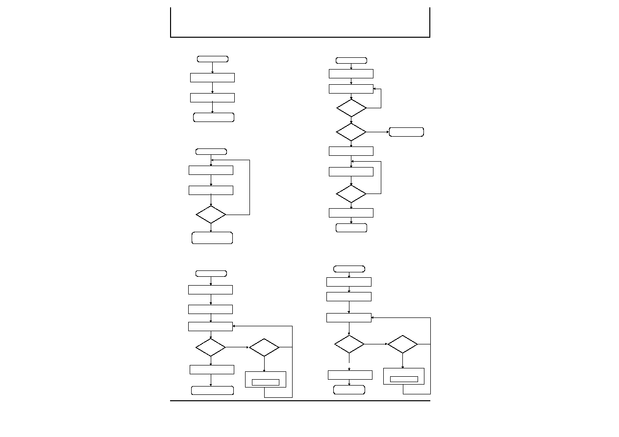
FULL STATUS CHECK PROCEDURE
SR.5 = 0 ?
SR.4 = 0 ?
SR.4 =1
and
SR.5 =1
?
SUCCESSFUL
(BLOCK ERASE, PROGRAM)
YES
YES
YES
NO
STATUS REGISTER
READ
COMMAND SEQUENCE ERROR
NO
BLOCK ERASE ERROR
NO
PROGRAM ERROR
(BLOCK)
WRITE 77H
WRITE D0H
BLOCK ADDRESS
LOCK BIT PROGRAM FLOW CHART
SR.4 = 0 ?
LOCK BIT PROGRAM
SUCCESSFUL
YES
YES
NO
NO
START
LOCK BIT PROGRAM
FAILED
SR.7 = 1 ?
SR.3 = 0 ?
YES
NO
PROGRAM ERROR
(PAGE, LOCK BIT)
PAGE PROGRAM FLOW CHART
START
WRITE 41H
FULL STATUS CHECK
IF DESIRED
PAGE PROGRAM
COMPLETED
YES
n = 0
n = n+1
WRITE
ADDRESS n, DATA n
YES
SR.7 = 1 ?
n = FFH ?
or
n = 7FH ?
NO
WRITE B0H ?
YES
NO
SUSPEND LOOP
WRITE D0H
YES
NO
STATUS REGISTER
READ
BYTE PROGRAM FLOW CHART
START
WRITE 40H
FULL STATUS CHECK
IF DESIRED
PAGE PROGRAM
COMPLETED
YES
WRITE
ADDRESS , DATA
SR.7 = 1 ?
WRITE B0H ?
YES
NO
SUSPEND LOOP
WRITE D0H
YES
NO
STATUS REGISTER
READ
* Word program is admitted to only BANK(I).
MITSUBISHI LSIs
16,777,216-BIT (1048,576-WORD BY16-BIT)
CMOS 3.3V-ONLY, BLOCK ERASE FLASH MEMORY
M5M29GB/T161BWG
Sep.1999. Rev4.0
22
SUSPEND / RESUME FLOW CHART
START
WRITE B0H
OPERATION
RESUMED
SR.6 =1?
YES
NO
WRITE FFH
READ ARRAY DATA
DONE
READING ?
NO
YES
WRITE D0H
SUSPEND
RESUME
BLOCK ERASE FLOW CHART
START
WRITE 20H
WRITE D0H
BLOCK ADDRESS
FULL STATUS CHECK
IF DESIRED
YES
SR.7 = 1 ?
WRITE B0H ?
YES
NO
SUSPEND LOOP
WRITE D0H
YES
NO
STATUS REGISTER
READ
BLOCK ERASE
COMPLETED
STATUS REGISTER
READ
SR.7 = 1?
YES
NO
PROGRAM / ERASE
COMPLETED
* The bank address is required when writing this command. Also, there is
no need to suspend the erase or program operation when reading data
from the other bank. Please use BGO function.
SINGLE DATA LOAD TO PAGE BUFFER
START
WRITE 74H
FULL STATUS CHECK
IF DESIRED
PAGE BUFFER TO FLASH
COMPLETED
WRITE
ADDRESS , DATA
WRITE B0H ?
YES
NO
SUSPEND LOOP
WRITE D0H
YES
NO
STATUS REGISTER
READ
WRITE 0EH
WRITE D0H
PAGE ADDRESS
SR.7 = 1 ?
YES
DONE
LOADING?
NO
SINGLE DATA LOAD
TO PAGE BUFFER
COMPLETED
PAGE BUFFER TO FLASH
START
CLEAR PAGE BUFFER
START
WRITE 55H
WRITE D0H
PAGE BUFFER CLEAR
COMPLETED

MITSUBISHI LSIs
16,777,216-BIT (1048,576-WORD BY16-BIT)
CMOS 3.3V-ONLY, BLOCK ERASE FLASH MEMORY
M5M29GB/T161BWG
Sep.1999. Rev4.0
23
OPERATION STATUS and EFFECTIVE COMMAND
Page Program
Setup
Lock Bit Program
Setup
Block Erase
Setup
Setup State
Read/Standby State
OTHER
Erase &
Verify
Read
Status Register
B0H
D0H
B0H
D0H
50H
41H
77H
20H
A7H
Suspend State
Read Array
Read
Status Register
FFH
70H
70H
Read
Status Register
Read
Device Identifier
Read
Lock Status
FFH
70H
90H
70H
90H
FFH
FFH
71H
70H
71H
90H
Read Array
OTHER
OTHER
D0H
D0H
D0H
WDi
i=0-127
Erase All Unlocked
Blocks Setup
Program &
Verify
Read
Status Register
71H
Clear
Status Register
Ready
Read Array
(From The Other Bank)
Change Bank
Address
Change Bank
Address
Read State with BGO
40H
Byte Program
Setup
WD
0EH
D0H
Single Data Load
to Page Buffer
Setup
74H
WD
OTHER
Page Buffer to Flash
Setup
Internal State
Clear
Page Buffer
Setup
55H
D0H