MITSUBISHI ICs (Monitor)
M52733SP
3-CHANNEL VIDEO AMPLIFICATION WITH OSD BLANKING
1
DESCRIPTION
The M52733SP is a semiconductor integrated circuit amplifies
video signals, having a 3-channel amplifier with a band width of
130MHz. The circuit also features the OSD blanking function.
The circuit is most useful with high resolution displays that have
OSD, and its function are available for each channel, including OSD
blanking, wide-band amplification, contrast control (main and sub),
and brightness control.
FEATURES
·
Frequency band width: RGB................................130MHz (3V
P-P
)
Input
:RGB.............................................................0.7V
P-P
(typ.)
BLK ...............................................3.0V
P-P
min. (positive)
Output :RGB...........................................................4.0V
P-P
(max.)
·
To adjust contrast, two types of controls are provided, main and
sub. With the main control, the contrast of the 3-channels can be
changed simultaneously. Sub controls are used to adjust the
contrast of a given channel individually. The control terminals can
be controlled by applying a voltage of 0 to 5V.
·
The DC power remains stable at the IC output terminal because
a feedback circuit is built in.
APPLICATION
Display monitor
RECOMMENDED OPERATING CONDITION
Supply voltage range....................................................11.5 to 12.5V
Rated supply voltage................................................................12.0V
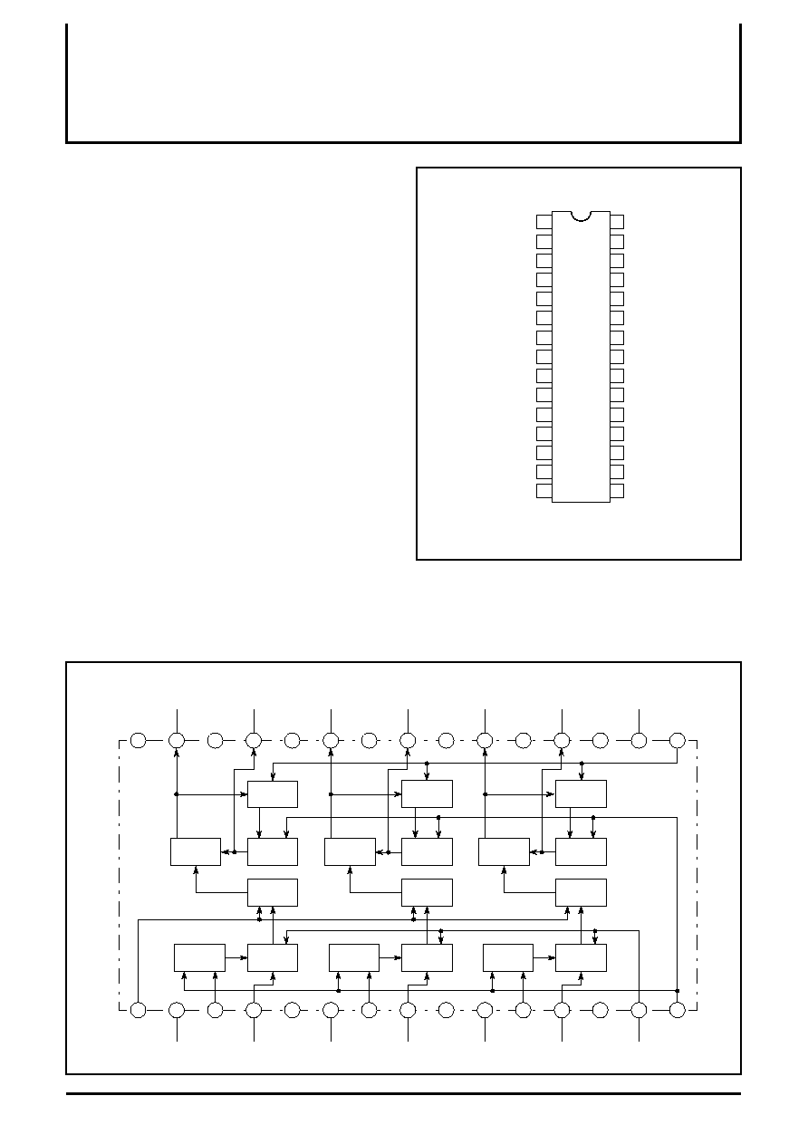
PIN CONFIGURATION (TOP VIEW)
Outline 30P4B
30
27
28
29
1
4
3
2
26
5
25
6
22
9
21
10
20
11
19
18
12
13
14
17
7
8
24
23
15
16
OUTPUT (G)
V
CC2
(B)
HOLD (B)
OUTPUT (R)
OUTPUT (B)
GND2 (B)
V
CC2
(G)
INPUT (B)
V
CC1
(G)
SUB CONTRAST (B)
GND1 (G)
GND1 (B)
V
CC1
(B)
V
CC1
(R)
SUB CONTRAST (G)
OSD BLK IN
GND
GND2 (G)
INPUT (G)
HOLD (G)
NC
GND2 (R)
HOLD (R)
GND1 (R)
MAIN CONTRAST
SUB CONTRAST (R)
INPUT (R)
V
CC2
(R)
NC : NO CONNECTION
M52733SP
CP IN
BRIGHTNESS
BLOCK DIAGRAM
B
Hold
B
Blanking
B
Contrast
G
G
G
G
R
R
R
R
OUTPUT (G)
V
CC2
(B)
HOLD (B)
OUTPUT (R)
OUTPUT (B)
GND2 (B)
SUB CONTRAST
INPUT (G)
GND1 (B)
V
CC1
(R)
V
CC1
(G)
INPUT (B)
INPUT (R)
GND1 (G)
V
CC1
(B)
GND
GND2 (G)
SUB CONTRAST
HOLD (G)
NC
BRIGHTNESS
HOLD (R)
MAIN CONTRAST
CP IN
GND1 (R)
SUB CONTRAST
V
CC2
(R)
(R)
(G)
(B)
GND2 (R)
28
26
27
25
24
20
21
19
17
18
23
22
1
3
2
4
5
9
8
10
12
11
13
14
6
7
15
29
30
B
AMP
B
Clamp
G
G
R
R
B
Brightness
16
V
CC2
(G)
OSD BLK IN
Hold
Blanking
Contrast
AMP
Clamp
Brightness
Hold
Blanking
Contrast
AMP
Clamp
Brightness
MITSUBISHI ICs (Monitor)
M52733SP
3-CHANNEL VIDEO AMPLIFICATION WITH OSD BLANKING
2
ABSOLUTE MAXIMUM RATINGS
(Ta=25
°
C)
ELECTRICAL CHARACTERISTICS
(V
CC
=12V, Ta=25
°
C, unless otherwise noted)
Symbol
Parameter
Ratings
Unit
V
CC
Supply voltage
13.0
V
P
d
Power dissipation
1736
mW
T
opr
Ambient temperature
-20 to +85
°
C
T
stg
Storage temperature
-40 to +150
°
C
V
opr
Recommended supply voltage
12.0
V
V
opr'
Recommended supply voltage range
11.5 to 12.5
V
Surge
Electrostatic discharge
±
200
V
Symbol
Parameter
Test conditions
Limits
Unit
Test
point
(s)
Input
External power supply (V)
Pulse input
SW11
R-ch
SW7
G-ch
SW3
B-ch
V4
V14
V16
SW1 SW15
Min.
Typ.
Max.
I
CC
Circuit current
A
a
-
a
-
a
-
5
5
5
a
-
b
SG5
60
83
123
mA
Vomax
Output dynamic range
T.P.29
T.P.25
T.P.21
b
SG6
b
SG6
b
SG6
5
5
Vari-
able
a
-
b
SG5
5.8
6.8
9.0
V
P-P
Vimax
Maximum input
T.P.29
T.P.25
T.P.21
b
SG6
b
SG6
b
SG6
5
2.5
1
a
-
b
SG5
1
1.8
-
V
P-P
Gv
Maximum gain
T.P.29
T.P.25
T.P.21
b
SG6
b
SG6
b
SG6
5
5
2
a
-
b
SG5
15
17
20
dB
Gv
Rrlative maximum gain
Relative to measured values above
0.8
1
1.2
-
V
CR1
Contrast control
characteristics (typical)
T.P.29
T.P.25
T.P.21
b
SG6
b
SG6
b
SG6
5
4
2
a
-
b
SG5
14
15.5
17
dB
V
CR1
Contrast control relative
characteristics (typical)
Relative to measured values above
0.8
1
1.2
-
V
CR2
Contrast control
characteristics
(minimum)
T.P.29
T.P.25
T.P.21
b
SG6
b
SG6
b
SG6
5
1
2
a
-
b
SG5
0.3
0.6
0.9
V
P-P
V
CR2
Contrast control relative
characteristics (minimum)
Relative to measured values above
0.8
1
1.2
-
V
SCR1
Sub contrast control
characteristics (typical)
T.P.29
T.P.25
T.P.21
b
SG6
b
SG6
b
SG6
4
5
2
a
-
b
SG5
14
15.5
17
dB
V
SCR1
Sub contrast control
relative characteristics
(typical)
Relative to measured values above
0.8
1
1.2
-
V
SCR2
Sub contrast control
characteristics
(minimum)
T.P.29
T.P.25
T.P.21
b
SG6
b
SG6
b
SG6
1
5
2
a
-
b
SG5
0.5
0.9
1.3
V
P-P
V
SCR2
Sub contrast control relative
characteristics (minimum)
Relative to measured values above
0.8
1
1.2
-
V
SCR3
Contrast/sub contrast
control characteristics
(typical)
T.P.29
T.P.25
T.P.21
b
SG6
b
SG6
b
SG6
3
3
2
a
-
b
SG5
0.8
1.5
2.2
V
P-P
V
SCR3
Contrast/sub contrast
control relative
characteristics (typical)
Relative to measured values above
0.8
1
1.2
-
V
B1
Brightness control
characteristics
(maximum)
T.P.29
T.P.25
T.P.21
a
-
a
-
a
-
5
5
4
a
-
b
SG5
3.0
3.6
4.2
V
V
B1
Brightness control relative
characteristics (maximum)
Relative to measured values above
-0.3
0
0.3
V

MITSUBISHI ICs (Monitor)
M52733SP
3-CHANNEL VIDEO AMPLIFICATION WITH OSD BLANKING
3
ELECTRICAL CHARACTERISTICS
(cont.)
Symbol
Parameter
Test conditions
Limits
Unit
Test
point
(s)
Input
External power supply (V
)
Pulse input
SW11
R-ch
SW7
G-ch
SW3
B-ch
V4
V14
V16
SW1 SW15
Min.
Typ.
Max.
V
B2
Brightness control
characteristics (typical)
T.P.29
T.P.25
T.P.21
a
-
a
-
a
-
5
5
2.5
a
-
b
SG5
1.7
2.3
2.9
V
V
B2
Brightness control relative
characteristics (typical)
Relative to measured values above
-0.3
0
0.3
V
V
B3
Brightness control
characteristics
(minimum)
T.P.29
T.P.25
T.P.21
a
-
a
-
a
-
5
5
1
a
-
b
SG5
0.5
0.9
1.3
V
V
B3
Brightness control relative
characteristics (minimum)
Relative to measured values above
-0.3
0
0.3
V
F
C1
Frequency
characteristics 1
(f=50MHz)
T.P.29
T.P.25
T.P.21
b
SG2
b
SG2
b
SG2
5
2.5
V
T
a
-
a
-
-2.5
-1
3
dB
F
C1
Frequency relative
characteristics 1 (f=50MHz)
Relative to measured values above
-1
0
1
dB
F
C1'
Frequency
characteristics 1
(f=130MHz;maximum)
T.P.29
T.P.25
T.P.21
b
SG3
b
SG3
b
SG3
5
2.5
V
T
a
-
a
-
-3
-2
3
dB
F
C1'
Frequency relative
characteristics 1
(f=130MHz;maximum)
Relative to measured values above
-1
0
1
dB
F
C2
Frequency
characteristics 2
(f=130MHz; maximum)
T.P.29
T.P.25
T.P.21
b
SG3
b
SG3
b
SG3
5
1.5
V
T
a
-
a
-
-3
0
3
dB
F
C2'
Frequency relative
characteristics 2
(f=130MHz; maximum)
Relative to measured values above
-1
0
1
dB
C.T.1
Crosstalk 1 (f=50MHz)
T.P.29
T.P.25
T.P.21
b
SG2
a
-
a
-
5
5
V
T
a
-
a
-
-
-30
-20
dB
C.T.1'
Crosstalk 1 (f=130MHz)
T.P.29
T.P.25
T.P.21
b
SG3
a
-
a
-
5
5
V
T
a
-
a
-
-
-20
-15
dB
C.T.2
Crosstalk 2 (f=50MHz)
T.P.29
T.P.25
T.P.21
a
-
b
SG2
a
-
5
5
V
T
a
-
a
-
-
-30
-20
dB
C.T.2'
Crosstalk 2 (f=130MHz)
T.P.29
T.P.25
T.P.21
a
-
b
SG3
a
-
5
5
V
T
a
-
a
-
-
-20
-15
dB
C.T.3
Crosstalk 3 (f=50MHz)
T.P.29
T.P.25
T.P.21
a
-
a
-
b
SG2
5
5
V
T
a
-
a
-
-
-30
-20
dB
C.T.3'
Crosstalk 3 (f=130MHz)
T.P.29
T.P.25
T.P.21
a
-
a
-
b
SG3
5
5
V
T
a
-
a
-
-
-20
-15
dB
Tr
Pulse characteristics 1
T.P.29
T.P.25
T.P.21
b
SG4
b
SG4
b
SG4
5
3.3
2
a
-
b
SG5
-
3
7
nsec
Tf
Pulse characteristics 2
T.P.29
T.P.25
T.P.21
b
SG4
b
SG4
b
SG4
5
3.3
2
a
-
b
SG5
-
4
8
nsec
V14th
Clamp pulse threshold
voltage
T.P.29
T.P.25
T.P.21
a
-
a
-
a
-
5
5
2
a
-
b
SG5
1.0
1.5
2.0
V
DC
W14
Clamp pulse minimum
width
T.P.29
T.P.25
T.P.21
a
-
a
-
a
-
5
5
2
a
-
b
SG5
-
0.1
0.5
µ
sec
P
DCH
Pedestal voltage
temperatere
characteristics1
T.P.29
T.P.25
T.P.21
b
SG6
b
SG6
b
SG6
5
5
2
a
-
b
SG5
-0.3
0
0.3
V
DC
MITSUBISHI ICs (Monitor)
M52733SP
3-CHANNEL VIDEO AMPLIFICATION WITH OSD BLANKING
4
ELECTRICAL CHARACTERISTICS TEST METHOD
1. Because a description of signal input pin and pulse input pin
switch numbers is already given in Supplementary Table, only
external power supply switch numbers are included in the notes
below.
Sub contrast voltages V4, V8 and V12 are always set to the
same voltage, therefore only V4 is referred to in Supplementary
Table.
I
CC
Circuit current
Measuring conditions are as listed in Supplementary Table.
Measured with an ammeter At test point A when SW A is set to b.
Vomax Output dynamic range
Voltage V16 is varied as described below:
1. Increase V16 gradually while inputting SG6 to pin 11 (7 or 3).
Measure the voltage when the top of the waveform output at
T.P21 (25 or 29) is distorted. The voltage is called V
TR1
(V
TG1
or
V
TB1
). Next, decrease V16 gradually, and measure the voltage
when the bottom of the waveform output at T.P29 (25 or 21) is
distorted. The voltage is called V
TR2
(V
TG2
or V
TB2
).
2. Voltage V
T
(V
TR
, V
TG
and V
TB
) is calculated by the equation
below:
Use relevant voltages, depending on the pin at which the
waveform is output; specifically, use V
TR1
when it is output at
T.P21; V
TG1
, at T.P25, and V
TB
, at T.P29.
3. After setting V
TR
(V
TG
or V
TB
), increase the SG6 amplitude
gradually, starting from 700mV. Measure the amplitude when the
top and bottom of the waveform output at T.P21 (25 or 29) starts
becoming distorted synchronously.
Vimax Maximum input
Measuring conditions are the same as those used above, except
that the setting of V14 is changed to 2.5V as specified in
Supplementary Table. Increase the input signal amplitude gradually,
starting from 700mV
P-P
.
Measure the amplitude when the output
signal starts becoming distorted.
Gv Maximum gain
Gv Relative maximum gain
1. Input SG6 to pin 11 (7 or 3), and read the amplitude at output
T.P21 (25 or 29). The amplitude is called V
OR1
(V
OG1
or V
OB1
) .
2. Maximum gain G
V
is calculated by the equation below:
3. Relative maximum gain
G is calculated by the equation below:
G
V
=V
OR1
/V
OG1
, V
OG1
/V
OB1
, V
OB1
/V
OR1
V
CR1
Contrast control characteristics (typical)
V
CR1
Contrast control relative characteristics (typical)
1. Measuring conditions are as given in Supplementary Table.
The setting of V14 is changed to 4V.
2. Measure the amplitude output at T.P21 (25 or 29). The measured
value is called V
OR2
(V
OG2
or V
OB2
).
3. Contrast control characteristics V
CR1
and relative characteristics
V
CR1
are calculated, respectively, by the equations below:
V
CR1
=V
OR2
/V
OG2
, V
OG2
/V
OB2
, V
OB2
/V
OR2
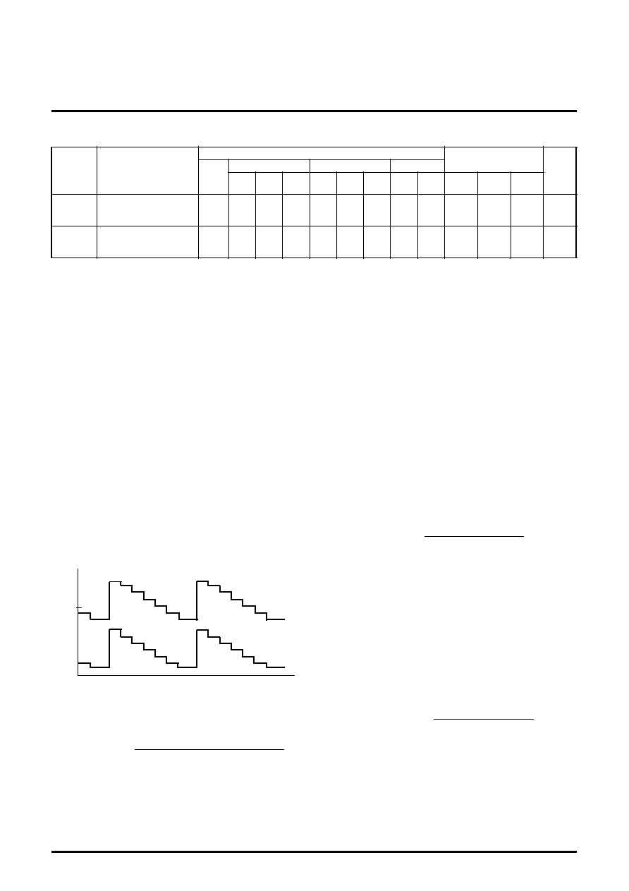
Waveform Output at T.P21
(Identical to output at T.P25 and T.P29.)
0.0
5.0
(V)
V
TR1
(V
TG1
, V
TB1
) + V
TR2
(V
TG1
, V
TB1
)
2
V
TR
(V
TG
, V
TB
)=
V
OR1
(V
OG1
, V
OB1
)
0.7
[V
P-P
]
[V
P-P
]
G
V
=20LOG
V
OR2
(V
OG2
, V
OB2
)
0.7
[V
P-P
]
[V
P-P
]
V
CR1
=20LOG
ELECTRICAL CHARACTERISTICS
(cont.)
Symbol
Parameter
Test conditions
Limits
Unit
Test
point
(s)
Input
External power supply (V
)
Pulse input
SW11
R-ch
SW7
G-ch
SW3
B-ch
V4
V14
V16
SW1 SW15
Min.
Typ.
Max.
P
DCL
Pedestal voltage
temperatere
characteristics2
T.P.29
T.P.25
T.P.21
b
SG6
b
SG6
b
SG6
5
5
2
a
-
b
SG5
-0.3
0
0.3
V
DC
V1th
BLK input threshold
voltage
T.P.29
T.P.25
T.P.21
b
SG6
b
SG6
b
SG6
5
5
2
b
SG7
b
SG5
1.7
2.5
3.5
V
DC

MITSUBISHI ICs (Monitor)
M52733SP
3-CHANNEL VIDEO AMPLIFICATION WITH OSD BLANKING
5
V
CR2
Contrast control characteristics (minimum)
V
CR2
Contrast control relative characteristics (minimum)
1. Measuring conditions are as given in Supplementary Table.
The setting of V14 is changed to 1.0V.
2. Measure the amplitude output at T.P21 (25 or 29). The measured
value is called V
OR3
(V
OG3
or V
OB3
), and is treated as V
CR2
.
3. Contrast control relative characteristics
V
CR2
are calculated by
the equation below:
V
CR2
=V
OR3
/V
OG3
, V
OG3
/V
OB3
, V
OB3
/V
OR3
V
SCR1
Sub contrast control characteristics (typical)
V
SCR1
Sub contrast control relative characteristics (typical)
1. Set V4, V8 and V12 to 4.0V. Other conditions are as given in
Supplementary Table.
2. Measure the amplitude output at T.P21 (25 or 29). The measured
value is called V
OR4
(V
OG4
or V
OB4
).
3. Sub contrast control characteristics V
SCR1
and relative
characteristics
V
SCR1
are calculated, respectively, by the
equations below:
V
SCR1
=V
OR4
/V
OG4
, V
OG4
/V
OB4
, V
OB4
/V
OR4
V
SCR2
Sub contrast control characteristics (minimum)
V
SCR2
Sub contrast control relative characteristics (minimum)
1. Set V4, V8 and V12 to 1.0V. Other conditions are as given in
Supplementary Table.
2. Measure the amplitude output at T.P21 (25 or 29). The measured
value is called V
OR5
(V
OG5
or V
OB5
).
3. Relative characteristics
V
SCR2
are calculated by the equation
below:
V
SCR2
=V
OR5
/V
OG5
, V
OG5
/V
OB5
, V
OB5/
V
OR5
V
SCR3
Contrast/sub contrast control characteristics (typical)
V
SCR3
Contrast/sub contrast control relative
characteristics (typical)
1. Set V4, V8, V12 and V14 to 3.0V. Other conditions are as given
in Supplementary Table.
2. Measure the amplitude at T.P21 (25 or 29). The measured value
is called V
OR6
(V
OG6
or V
OB6
).
V
CR3
=V
OR6
/V
OG6
, V
OG6
/V
OB6
, V
OB6
/V
OR6
V
B1
Brightness control characteristics (maximum)
V
B1
Brightness control relative characteristics (maximum)
1. Measuring conditions are as given in Supplementary Table.
2. Measure the output at T.P21 (25 or 29) with a voltmeter.
The measured value is called V
OR7
(V
OG7
or V
OB7
), and is treated
as V
B1
.
3. To obtain brightness control relative characteristics, calculate the
difference in the output between the channels, using V
OR7
, V
OG7
and V
OB7
.
V
B1
=V
OR7
-V
OG7
[mV]
=V
OG7
-V
OB7
=V
OB7
-V
OR7
V
B2
Brightness control characteristics (typical)
V
B2
Brightness control relative characteristics (typical)
1. Measuring conditions are as given in Supplementary Table.
2. Measure the output at T.P21 (25 or 29) with a voltmeter.
The measured value is called V
OR7'
(V
OG7'
or V
OB7'
), and is
treated as V
B2
.
3. To obtain brightness control relative characteristics (
V
B2
),
calculate the difference in the output between the channels,
using V
OR7'
, V
OG7'
, and V
OB7'
.
V
B2
=V
OR7'
-V
OG7'
[mV]
=V
OG7'
-V
OB7'
=V
OB7'
-V
OR7'
V
B3
Brightness control characteristics (minimum)
V
B3
Brightness control relative characteristics (minimum)
1. Measuring conditions are as given in Supplementary Table.
2. Measure the output at T.P21 (25 or 29) with a voltmeter.
The measured value is called V
OR7"
(V
OG7"
or V
OB7"
), and is
treated as V
B2
.
3. To obtain brightness control relative characteristics (
V
B3
),
calculate the difference in the output between the channels,
using V
OR7"
, V
OG7"
and V
OB7"
.
V
B3
=V
OR7''
-V
OG7''
[mV]
=V
OG7''
-V
OB7''
=V
OB7''
-V
OR7''
F
C1
Frequency characteristics1 (f=50MHz)
F
C1
Frequency relative characteristics1
(f=50MHz)
F
C1
' Frequency characteristics1 (f=130MHz; maximum)
F
C1
' Frequency relative characteristics1
(f=130MHz; maximum)
1. Measuring conditions are as given in Supplementary Table.
2. SG2 and SG3 are input. The amplitude of the waveform output at
T.P21 (25 or 29) is measured by the same procedure as in G
V
,
G
V
.
V
OR4
(V
OG4
, V
OB4
)
0.7
[V
P-P
]
[V
P-P
]
V
SCR1
=20LOG
V
OR6
(V
OG6
, V
OB6
)
0.7
[V
P-P
]
[V
P-P
]
V
CR3
=20LOG