MITSUBISHI ICs (Monitor)
M52732SP
3-CHANNEL VIDEO AMPLIFICATION
1
DESCRIPTION
The M52732SP is a semiconductor integrated circuit that has 3-
channels of built-in amplifiers in the broad-band video amplifier
having a 75MHz band. Every channel is provided with a broad-band
amplifier, contrast control (main and sub), and brightness control. It
accordingly has an optimal configuration for use with high
resolution color display monitors.
FEATURES
·
It realize low power dissipation so that 3-channels are built in.
(V
CC
=12V, I
CC
=63mA)
·
Input..........................................................................0.7V
P-P
(typ.)
Output.....................................................................4.5V
P-P
(max.)
Frequency band.................................................75MHz (at 3V
P-P
)
·
To adjust contrast, two types of controls are provided, main and
sub.
The main controls adjusts 3-channels of contrast concurrently.
The sub contrast controls adjusts either channel independentry.
APPLICATION
Display monitor
RECOMMENDED OPERATING CONDITION
Supply voltage range....................................................11.5 to 12.5V
Rated supply voltage................................................................12.0V
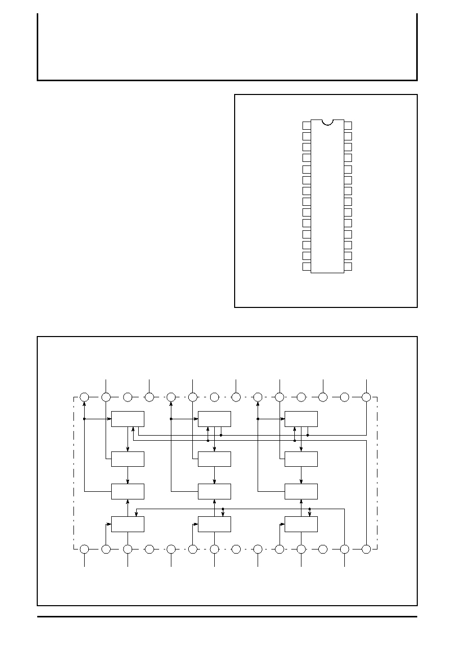
PIN CONFIGURATION (TOP VIEW)
28
25
26
27
1
4
3
2
24
5
23
6
20
9
19
10
18
11
17
16
12
13
14
15
7
8
22
21
Outline 28P4B
HOLD (G)
NC
GND (B)
HOLD (R)
HOLD (B)
OUTPUT (G)
NC
SUB CONTRAST
INPUT (G)
GND (B)
V
CC
(R)
V
CC
(G)
INPUT (B)
INPUT (R)
GND (G)
V
CC
(B)
OUTPUT (B)
OUTPUT (R)
SUB CONTRAST
GND (G)
V
CC
BRIGHTNESS
GND (R)
MAIN CONTRAST
CP IN
GND (R)
SUB CONTRAST
NC
NC : NO CONNECTION
M52732SP
CONTROL
CONTROL (R)
CONTROL (G)
CONTROL (B)
CONTROL
BLOCK DIAGRAM
B-ch
Brt
B-ch
Hold
B-ch
Amp
B-ch
CONTRAST
G-ch
Brt
G-ch
Hold
G-ch
Amp
G-ch
CONTRAST
R-ch
Brt
R-ch
Hold
R-ch
Amp
R-ch
CONTRAST
HOLD(G)
NC
GND (B)
HOLD (R)
HOLD (B)
OUTPUT (G)
NC
SUB CONTRAST
INPUT (G)
GND (B)
V
CC
(R)
V
CC
(G)
INPUT (B)
INPUT (R)
GND (G)
V
CC
(B)
OUTPUT (B)
OUTPUT (R)
SUB CONTRAST
GND (G)
V
CC
BRIGHTNESS
GND (R)
MAIN CONTRAST
CP IN
GND (R)
SUB CONTRAST
NC
CONTROL
CONTROL (R)
CONTROL (G)
CONTROL (B)
CONTROL
28
26
27
25
24
20
21
19
17
18
16
15
23
22
1
3
2
4
5
9
8
10
12
11
13
14
6
7

MITSUBISHI ICs (Monitor)
M52732SP
3-CHANNEL VIDEO AMPLIFICATION
2
ABSOLUTE MAXIMUM RATINGS
(Ta=25
°
C)
ELECTRICAL CHARACTERISTICS
(V
CC
=12V, Ta=25
°
C, unless otherwise noted)
Symbol
Parameter
Ratings
Unit
V
CC
Supply voltage
13.0
V
P
d
Power dissipation
1580
mW
T
opr
Ambient temperature
-20 to +85
°
C
T
stg
Storage temperature
-40 to +150
°
C
V
opr
Recommended supply voltage
12.0
V
V
opr'
Recommended supply voltage range
11.5 to 12.5
V
Surge
Electrostatic discharge
±
200
V
Symbol
Parameter
Test conditions
Limits
Unit
Test
point (s)
Input
External power supply (V)
Pulse
input
SW10
R-ch
SW6
G-ch
SW2
B-ch
V3
V13
V15
SW14
Min.
Typ.
Max.
I
CC
Circuit current
A
a
-
a
-
a
-
12
12
5
b
SG6
45
72
110
mA
Vomax
Output dynamic range
T.P.20
T.P.24
T.P.28
b
SG1
b
SG1
b
SG1
12
12
Variable
a
-
5.8
6.8
9.0
V
P-P
Vimax
Maximum input
T.P.20
T.P.24
T.P.28
b
SG1
b
SG1
b
SG1
12
6
Variable
a
-
1.9
2.4
2.9
V
P-P
Gv
Maximum gain
T.P.20
T.P.24
T.P.28
b
SG1
b
SG1
b
SG1
12
12
V
T
a
-
13
17
20
dB
Gv
Relative maximum gain
Relative to measured values above
0.8
1
1.2
-
V
CR1
Contrast control
characteristics (typical)
T.P.20
T.P.24
T.P.28
b
SG1
b
SG1
b
SG1
12
6
V
T
a
-
4.0
7.4
10.1
dB
V
CR1
Contrast control relative
characteristics (typical)
Relative to measured values above
0.8
1
1.2
-
V
CR2
Contrast control
characteristics
(minimum)
T.P.20
T.P.24
T.P.28
b
SG1
b
SG1
b
SG1
12
3.5
V
T
a
-
5
30
70
mV
P-P
V
CR2
Contrast control relative
characteristics (minimum)
Relative to measured values above
0.8
1
1.3
-
V
SCR1
Sub contrast control
characteristics (typical)
T.P.20
T.P.24
T.P.28
b
SG1
b
SG1
b
SG1
6
12
V
T
a
-
9.9
14
18.1
dB
V
SCR1
Sub contrast control
relative characteristics
(typical)
Relative to measured values above
0.8
1
1.2
-
V
SCR2
Sub contrast control
characteristics
(minimum)
T.P.20
T.P.24
T.P.28
b
SG1
b
SG1
b
SG1
3
12
V
T
a
-
50
300
600
mV
P-P
V
SCR2
Sub contrast control relative
characteristics (minimum)
Relative to measured values above
0.8
1
1.2
-
V
CR2
Contrast/sub contrast
control characteristics
(typical)
T.P.20
T.P.24
T.P.28
b
SG1
b
SG1
b
SG1
6
6
V
T
a
-
0.9
1.3
1.7
V
P-P
V
CR2
Contrast/sub contrast
control relative
characteristics (typical)
Relative to measured values above
0.8
1
1.2
-
V
B1
Brightness control
characteristics
(maximum)
T.P.20
T.P.24
T.P.28
a
-
a
-
a
-
12
12
5.5
b
SG6
3.6
4.3
5.0
V
V
B1
Brightness control relative
characteristics (maximum)
Relative to measured values above
-100
0
100
mV

MITSUBISHI ICs (Monitor)
M52732SP
3-CHANNEL VIDEO AMPLIFICATION
3
ELECTRICAL CHARACTERISTICS
(cont.)
Symbol
Parameter
Test conditions
Limits
Unit
Test
point (s)
Input
External power supply (V)
Pulse
input
SW10
R-ch
SW6
G-ch
SW2
B-ch
V3
V13
V15
SW14
Min.
Typ.
Max.
V
B2
Brightness control
characteristics (typical)
T.P.20
T.P.24
T.P.28
a
-
a
-
a
-
12
12
5
b
SG6
3.0
3.7
4.4
V
V
B2
Brightness control relative
characteristics (typical)
Relative to measured values above
-100
0
100
mV
V
B3
Brightness control
characteristics
(minimum)
T.P.20
T.P.24
T.P.28
a
-
a
-
a
-
12
12
4.5
b
SG6
2.5
3.2
4.0
V
DC
V
B3
Brightness control relative
characteristics (minimum)
Relative to measured values above
-100
0
100
mV
F
C1
Frequency
characteristics 1
(f=50MHz;maximum)
T.P.20
T.P.24
T.P.28
b
SG3
b
SG3
b
SG3
12
7.5
V
T
a
-
-2
0
3
dB
F
C1
Frequency relative
characteristics 1
(f=50MHz;maximum)
Relative to measured values above
-1
0
1
dB
F
C1'
Frequency
characteristics 1
(f=75MHz;maximum)
T.P.20
T.P.24
T.P.28
b
SG4
b
SG4
b
SG4
12
7.5
V
T
a
-
-3
0
3
dB
F
C1'
Frequency relative
characteristics 1
(f=75MHz;maximum)
Relative to measured values above
-1
0
1
dB
F
C2
Frequency
characteristics 2
(f=50MHz; maximum)
T.P.20
T.P.24
T.P.28
b
SG3
b
SG3
b
SG3
12
5
V
T
a
-
-0.5
0
3
dB
F
C2'
Frequency relative
characteristics 2
(f=75MHz; maximum)
T.P.20
T.P.24
T.P.28
b
SG4
b
SG4
b
SG4
12
5
V
T
a
-
-0.5
0
3
dB
C.T.1
Crosstalk 1 (f=50MHz)
T.P.20
T.P.24
T.P.28
b
SG3
a
-
a
-
12
12
V
T
a
-
-
-36
-24
dB
C.T.1'
Crosstalk 1 (f=75MHz)
T.P.20
T.P.24
T.P.28
b
SG4
a
-
a
-
12
12
V
T
a
-
-
-28
-18
dB
C.T.2
Crosstalk 2 (f=50MHz)
T.P.20
T.P.24
T.P.28
a
-
b
SG3
a
-
12
12
V
T
a
-
-
-36
-24
dB
C.T.2'
Crosstalk 2 (f=75MHz)
T.P.20
T.P.24
T.P.28
a
-
b
SG4
a
-
12
12
V
T
a
-
-
-28
-18
dB
C.T.3
Crosstalk 3 (f=50MHz)
T.P.20
T.P.24
T.P.28
a
-
a
-
b
SG3
12
12
V
T
a
-
-
-36
-24
dB
C.T.3'
Crosstalk 3 (f=75MHz)
T.P.20
T.P.24
T.P.28
a
-
a
-
b
SG4
12
12
V
T
a
-
-
-28
-18
dB
Tr
Pulse characteristics 1
T.P.20
T.P.24
T.P.28
b
SG5
b
SG5
b
SG5
12
7
3
b
SG6
-
3
7
nsec
Tf
Pulse characteristics 2
T.P.20
T.P.24
T.P.28
b
SG5
b
SG5
b
SG5
12
7
3
b
SG6
-
6
9
nsec
V14th
Clamp pulse threshold
voltage
T.P.20
T.P.24
T.P.28
a
-
a
-
a
-
12
12
3
b
SG6
0.7
1.5
2.5
V
DC
W14
Clamp pulse minimum
width
T.P.20
T.P.24
T.P.28
a
-
a
-
a
-
12
12
3
b
SG6
-
0.3
1.5
µ
sec
V27
Hold voltage
T.P.20
T.P.24
T.P.28
a
-
a
-
a
-
12
12
3
b
SG6
4
5.2
6.4
V
DC
MITSUBISHI ICs (Monitor)
M52732SP
3-CHANNEL VIDEO AMPLIFICATION
4
ELECTRICAL CHARACTERISTICS TEST METHOD
1. About switch numbers (SW Nos.) since those for the signal and
pulse input pins are listed in Attached Table 1, the following
notes omit them. Only SW Nos. for the external power supply will
be indicated in the Notes.
2. since sub contrast voltges V3, V7, and V11, they are also set to
the same value, so that V3 in attached Table 1 represents all.
I
CC
Circuit current
Conditions shall be as indicated in Attached Table 1. Measure
these conditions using ampere meter A with SW1 set to a.
Vomax Output dynamic range
1. Follow the procedure below to set V15.
Input SG1 to pin 10 (pin 6, 2) and raise V15 slowly. Read the
voltage of V15 when the higher peak of output waveform of T.P20
(T.P24, 28) begins distortion. This voltage is V
TR1
(V
TG1
, V
TB1
)
Next, reduce V15 slowly. Read the voltage of V15 when the lower
peak of output waveform of T.P20 (T.P24, 28) begins distortion.
This voltage is V
TR2
(V
TG2
, V
TB2
).
From the above result, V
T
(V
TR
, V
TG
, V
TB
) is determined as
follows:
Change the procedure according to output pins.
Use V
TR1
when measuring T.P20. Similarly, V
TG1
for T.P24, V
TB1
for T.P28.
2. Set V15 to V
TR
(V
TG
, V
TB
), then slowly raise SG1 amplitude
starting from 700mV. Measure the output amplitude when the
higher and lower peaks of T.P20 (T.P24, T.P28) output waveform
simultaneously begin distortion.
Vimax Maximum input
Under the conditions in Note 2, vary V13 to 6.7V as indicated in
Attached Table 1, then slowly raise amplitude of the input signal
starting from 700mV
P-P
. Read the amplitude of the input signal
when the output signal begins distortion.
Gv Maximum gain
Gv Relative maximum gain
1. Under conditions in attached Table.
2. Input SG1 to pin 10 (pin 6, 2). Read amplitude of the output at
T.P20 (T.P24, 28), which is V
OR1
(V
OG1
, V
OB1
).
3. The maximum gain G is:
4. The maximum relative gain
G is calculated by the equation
below:
G
V
=V
OR1
/V
OG1
, V
OG1
/V
OB1
, V
OB1
/V
OR1
V
CR1
Contrast control characteristics (typical)
V
CR1
Contrast control relative characteristics (typical)
1. Conditions are identical with those in Attached Table except
setting V13 to 6.0V.
2. Then read amplitude of the output at T.P20 (T.P24, 28), which is
V
OR2
(V
OG2
, V
OB2
)
3. The contrast control characteristics V
CR1
and relative contrast
control characteristics
V
CR1
are calculated by the equations
below:
V
CR1
=V
OR2
/V
OG2
, V
OG2
/V
OB2
, V
OB2
/V
OR2
V
CR2
Contrast control characteristics (minimum)
V
CR2
Contrast control relative characteristics (minimum)
1. Conditions are identical with those in Attached Table except
setting V13 to 3.0V.
2. Then read amplitude of the output at T.P20 (T.P24, 28), which is
V
OR3
(V
OG3
, V
OB3
) and also V
CR2
.
3. The relative contrast control characteristics
V
CR2
is:
V
CR2
=V
OR3
/V
OG3
, V
OG3
/V
OB3
, V
OB3
/V
OR3
V
SCR1
Sub contrast control characteristics (typical)
V
SCR1
Sub contrast control relative characteristics (typical)
1. Conditions are identical with those in Attached Table except
setting V3, V7, and V11 to 6.0V.
2. Then read amplitude of the output at T.P20 (T.P24, 28), which is
V
OR4
(V
OG4
, V
OB4
).
3. The sub contrast control characteristics V
SCR1
and relative sub
contrast control characteristics
V
SCR1
are:
V
SCR1
=V
OR4
/V
OG4
, V
OG4
/V
OB4
, V
OB4
/V
OR4
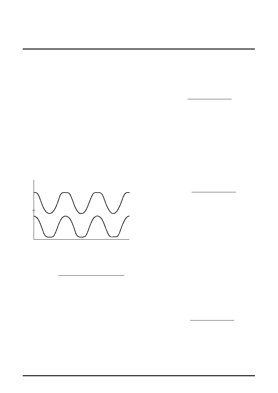
Waveform output at T.P20
(Identical to output at T.P24 and T.P28.)
0.0
(V)
5.0
V
TR1
(V
TG1
, V
TB1
) + V
TR2
(V
TG2
, V
TB2
)
2
V
TR
(V
TG
, V
TB
)=
V
OR1
(V
OG1
, V
OB1
)
0.7
[V
P-P
]
[V
P-P
]
GV=20LOG
V
OR2
(V
OG2
, V
OB2
)
0.7
[V
P-P
]
[V
P-P
]
V
CR1
=20LOG
V
OR4
(V
OG4
, V
OB4
)
0.7
[V
P-P
]
[V
P-P
]
V
SCR1
=20LOG

MITSUBISHI ICs (Monitor)
M52732SP
3-CHANNEL VIDEO AMPLIFICATION
5
V
SCR2
Sub contrast control characteristics (minimum)
V
SCR2
Sub contrast control relative characteristics (minimum)
1. Conditions are identical with those in Attached Table expect
setting V3, V7, and V11 to 3.0V.
2. Then read amplitude of the output at T.P20 (T.P24, 28), which is
V
OR5
(V
OG5
, V
OB5
) and also V
SCR2
.
3. The relative sub contrast control characteristics
V
SCR2
is:
V
SCR2
=V
OR5
/V
OG5
, V
OG5
/V
OB5
, V
OB5/
V
OR5
V
CR2
Contrast/sub contrast control characteristics (typical)
V
CR2
Contrast/sub contrast control relative
characteristics (typical)
1. Conditions are identical with those in Attached Table expect
setting V13, to 6.0V and V3, V7, and V11 to 6.0V.
2. Then read amplitude of the output at T.P20 (T.P24, 28), which is
V
OR6
(V
OG6
, V
OB6
).
3. The gain and relative gain when the contrast and sub contrast
are typical, are:
V
CR3
=V
OR6
/V
OG6
, V
OG6
/V
OB6
, V
OB6
/V
OR6
V
B1
Brightness control characteristics (maximum)
V
B1
Brightness control relative characteristics (maximum)
1. Under conditions in Attached Table.
2. Then use a voltmeter to measure the output at T.P20 (T.P24, 28),
which is V
OR7
(V
OG7
, V
OB7
). This value is V
B1
.
3. In addition, the relative brightness control characteristic is
determined from V
OR7
, V
OG7
, and V
OB7
by calculating differences
between each channel.
V
B1
=V
OR7
-V
OG7
=V
OG7
-V
OB7
[mV]
=V
OB7
-V
OR7
V
B2
Brightness control characteristics (typical)
V
B2
Brightness control relative characteristics (typical)
1. Under conditions in Attached Table.
2. Then use a voltmeter to measure the output at T.P20 (T.P24, 28),
which is V
OR7'
(V
OG7'
, V
OB7'
). This value is V
B2
.
3. In addition, the relative brightness control characteristic is
determined from V
OR7'
, V
OG7'
, and V
OB7'
by calculating
differences between each channel.
V
B2
=V
OR7'
-V
OG7'
=V
OG7'
-V
OB7'
[mV]
=V
OB7'
-V
OR7'
V
B3
Brightness control characteristics (minimum)
V
B3
Brightness control relative characteristics (minimum)
1. Under conditions in Attached Table.
2. Then use a voltmeter to measure the output at T.P20 (T.P24, 28),
which is V
OR7''
(V
OG7''
, V
OB7''
). This value is V
B3
.
3. In addition, the relative brightness control characteristic
V
B3
is
determined from V
OR7''
, V
OG7''
, and V
OB7''
by calculating
differences between each channel.
V
B3
=V
OR7''
-V
OG7''
=V
OG7''
-V
OB7''
[mV]
=V
OB7''
-V
OR7''
F
C1
Frequency characteristics1 (f=50MHz; maximum)
F
C1
Frequency relative characteristics1
(f=50MHz; maximum)
F
C1
' Frequency characteristics1
(f=75MHz; maximum)
F
C1
' Frequency relative characteristics1
(f=75MHz; maximum)
1. Under conditions in Attached Table.
2. Use SG3 and SG4. Measure amplitude of the output waveform
at T.P20 (T.P24, T.P28) following the procedure in G
V
,
G
V
.
3. The frequency characteristics F
C1
, F
C1'
are calculated by the
equations below:
Whre, V
OR8
(V
OG8
, V
OB8
) is the output amplitude when inputting
SG3, and V
OR9
(V
OG9
, V
OB9
), SG4, which are measured in 2
above. (V
OR1
(V
OG1
, V
OB1
) is the value measured in G
V
,
G
V
.)
4. The relative frequency characteristics
F
C1
,
F
C1'
are
determined by calculating differences between each channel's
F
C1
and F
C1'
.
F
C2
Frequency characteristics2 (f=50MHz; maximum)
F
C2
' Frequency relative characteristics2
(f=75MHz; maximum)
The procedure is identical with that in F
C1
,
F
C1
, F
C1'
,
F
C1'
except
that the contrast (V13) is reduced to 5.0V.
C.T.1 Crosstalk1 (f=50MHz)
C.T.1' Crosstalk1 (f=75MHz)
1. Under conditions in attached Table.
2. Input SG2 (or SG4) to pin 10 (R-ch) only. Then measure
amplitude of the output waveform at T.P20 (T.P24, T.P28), which
are V
OR
, V
OG
, and V
OB
, respectively.
3. Crosstalk C.T. is:
V
OR6
(V
OG6
, V
OB6
)
0.7
[V
P-P
]
[V
P-P
]
V
CR3
=20LOG
V
OR8
(V
OG8
, V
OB8
) [V
P-P
]
V
OR1
(V
OG1
, V
OB1
) [V
P-P
]
F
C1
=20LOG
V
OR9
(V
OG9
, V
OB9
) [V
P-P
]
V
OR1
(V
OG1
, V
OB1
) [V
P-P
]
F
C1'
=20LOG
V
OG
or V
OB
[V
P-P
]
V
OR
[V
P-P
]
[dB]
C.T. =20LOG
(C.T. ')