MITSUBISHI ICs (Monitor)
M52721SP
WIDEBAND VIDEO PREAMPLIFIER WITH OSD MIX
1
DESCRIPTION
The M52721SP is a wideband video preamplifier with 200MHz
band.
FEATURES
·
Input:0.7V
P-P
(Typical), Output:7V
P-P
(Maximum)
·
Maximum gain:20dB
·
Frequency band:200MHz (-3dB)
·
Contrast control (0 to 5V
DC
)
·
Brightness control (0 to 5V
DC
)
·
Built-in OSD MIX circuit
APPLICATION
Display monitor
RECOMMENDED OPERATING CONDITION
Supply voltage range....................................................11.5 to 12.5V
Rated supply voltage................................................................12.0V
Operating temperature..............................................-20
°
C to +85
°
C
Circuit current...........................................................................60mA
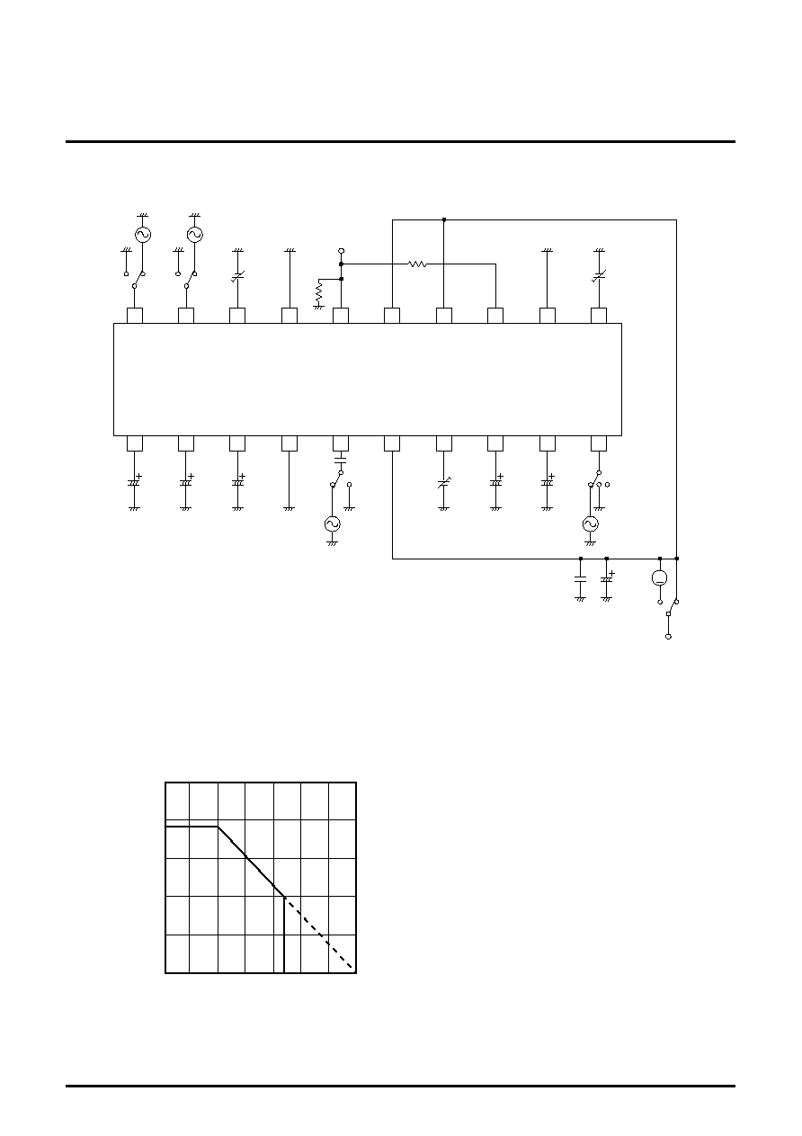
PIN CONFIGURATION (TOP VIEW)
CAP
REF.C
F.B.C
GND 1
VIDEO IN
V
CC1
CONTRAST
OSD.C
CLAMP
+
IN
OSD BLK IN
OSD MIX IN
OSD ADJUST
GND 3
VIDEO OUT
V
CC3
V
CC2
F/B
+
GND 2
F/B
Outline 20P4B
20
17
18
19
1
4
3
2
16
5
15
6
12
9
11
10
7
8
14
13
CLAMP HOLD
M52721SP
BLOCK DIAGRAM
CONTRAST
GND 1
V
CC1
CAP
11
12
13
14
15
16
17
18
19
20
10
9
8
7
6
5
4
3
2
1
CONTRAST
CLAMP
+
IN
CLAMP
OSD.C
VIDEO IN
F.B.C
REF.C
OSD
V
CC3
OSD
OSD
V
CC2
GND 3
VIDEO OUT
F/B
+
GND 2
F/B
HOLD
ADJUST
MIX IN
BLK IN
AMP
BRIGHTNESS
AMP
CLAMP
+

MITSUBISHI ICs (Monitor)
M52721SP
WIDEBAND VIDEO PREAMPLIFIER WITH OSD MIX
2
ABSOLUTE MAXIMUM RATINGS
(Ta=25
°
C, unless otherwise noted)
ELECTRICAL CHARACTERISTICS
(Ta=25
°
C, V
CC
=12V, unless otherwise noted)
Symbol
Parameter
Ratings
Unit
V
CC
Supply voltage
13.0
V
P
d
Power dissipation
1524
mW
T
opr
Operating temperature
-20 to +85
°
C
T
stg
Storage temperature
-40 to +150
°
C
V
opr
Recommended operating supply voltage
12.0
V
V
opr'
Recommended operating supply voltage range
11.5 to 12.5
V
Surge
Electrostatic discharge
±
200
V
Symbol
Parameter
Test
point
SWA
Test conditions
Limits
Unit
Input
External supply
voltage (V)
Pulse
SW5
V7
Con-
trast
V11
Bright-
ness
V18
OSD
Adj
SW10
Clamp
SW19
OSD
MIX
SW20
OSD
BLK
Min.
Typ.
Max.
I
CC
Circuit current
A
a
b
5.0
3.0
5.0
c
b
b
40
52
64
mA
V
omax
Output dynamic range
T.P16
b
a
SG8
5.0
0.5
0
a
SG6
b
b
8.0
8.9
11.5
V
P-P
V
imax
Maximum allowable input
T.P16
b
a
SG8
2.5
0.5
0
a
SG6
b
b
-
0.7
1.0
V
P-P
Gv
Maximum gain
T.P16
b
a
SG8
5.0
2.0
0
a
SG6
b
b
17.0
20.0
23.0
dB
V
CR1
Contrast control
characteristics 1
T.P16
b
a
SG8
2.5
2.0
0
a
SG6
b
b
13.0
15.0
17.0
dB
V
CR2
Contrast control
characteristics 2
T.P16
b
a
SG8
1.0
2.0
0
a
SG6
b
b
5.0
7.2
9.1
dB
V
B1
Brightness control
characteristics 1
T.P16
b
b
5.0
1.0
0
a
SG6
b
b
0.6
1.0
1.4
V
DC
V
B2
Brightness control
characteristics 2
T.P16
b
b
5.0
2.0
0
a
SG6
b
b
1.6
2.0
2.4
V
DC
V
B3
Brightness control
characteristics 3
T.P16
b
b
5.0
3.0
0
a
SG6
b
b
2.6
3.0
3.4
V
DC
F
1-a
Frequency
characteristics 1-a f=100MHz
T.P16
b
a
SG2
2.5
open
0
c
b
b
-1
0
3
dB
F
2-a
Frequency
characteristics 2-a f=200MHz
T.P16
b
a
SG3
2.5
open
0
c
b
b
-3
-2
3
dB
T
r
Pulse characteristics
(rise time)
T.P16
b
a
SG5
4
2.4
0
a
SG6
b
b
-
2.0
5.0
nsec
T
f
Pulse characteristics
(fall time)
T.P16
b
a
SG5
4
2.4
0
a
SG6
b
b
-
1.5
5.0
nsec
V
10th
Clamp pulse threshold voltage
T.P16
b
b
4
2.4
0
a
SG6
b
b
1.9
2.0
5.0
V
DC
W
10
Clamp pulse minimum width
T.P16
b
b
4
2.4
0
a
SG6
b
b
0.7
0.8
-
µ
sec
OT
r
OSD pulse characteristics
(rise time)
T.P16
b
b
4
2.4
4
a
SG6
a
SG7
b
-
5.0
10.0
nsec
OT
f
OSD pulse characteristics
(fall time)
T.P16
b
b
4
2.4
4
a
SG6
a
SG7
b
-
5.0
10.0
nsec
V
19th
OSD input threshold voltage
T.P16
b
b
4
2.4
4
a
SG6
a
SG7
b
2.2
2.3
5.0
V
DC
V
20th
BLK input threshold voltage
T.P16
b
a
SG8
4
2.4
4
a
SG6
b
a
SG7
2.8
2.9
5.0
V
DC
O
aj1
OSD adjust control
characteristics 1
T.P16
b
b
4
2.4
4
a
SG6
a
SG7
b
5.9
6.3
6.8
V
P-P
O
aj2
OSD adjust control
characteristics 2
T.P16
b
b
4
2.4
2
a
SG6
a
SG7
b
2.9
3.3
3.7
V
P-P
MITSUBISHI ICs (Monitor)
M52721SP
WIDEBAND VIDEO PREAMPLIFIER WITH OSD MIX
3
ELECTRICAL CHARACTERISTICS TEST METHOD
I
CC
Circuit current
When there is no signal, fix SWA on side "a", and measure I
CC
,
using ampere meter A.
V
omax
Output dynamic range
Input SG8 to pin 5, and set V11 at 0.5V
Gradually increase the amplitude of SG8 from 700mV, and
measure the amplitude of the TP16 output waveform when the
upper side of the waveform becomes distorted.
V
imax
Maximum allowable input
From the condition in Vomax above, change V7 to 2.5V, gradually
increase the amplitude of SG8 from 700mV
P-P
, and read the input
signal amplitude when the output signal starts to be distorted.
Gv Maximum gain
Read the amplitude of TP16 output: it should be taken as V
0
.
The maximum gain G
V
is determined by:
V
CR1
Contrast control characteristics 1
Set V7 at 2.5V, and read the amplitude of TP16 output: it should be
taken as V
01
.
V
CR2
Contrast control characteristics 2
Set V7 at 1.0V, and read the amplitude of TP16 output: it should be
taken as V
02
.
V
B1
Brightness control characteristics 1
Set brightness (V11) at 1.0V, and measure the output of TP16 with
a voltmeter. This value is V
B1
.
V
B2
Brightness control characteristics 2
Set brightness (V11) at 2.0V, and measure the output of TP16 with
a voltmeter. This value is V
B2
.
V
B3
Brightness control characteristics 3
Set brightness (V11) at 3.0V, and measure the output of TP16 with
a voltmeter. This value is V
B3
.
F
1-a
Frequency characteristics 1-a
f=100MHz
F
2-a
Frequency characteristics 2-a f=200MHz
With zero resistance between pins 13 and 16, apply a DC voltage to
pin 5 so that the bottom of the input waveform reaches 2.6V. Next,
apply a DC voltage to pin 8 so that the bottom of the output
waveform reaches 2.4V.
Input SG1 and measure the amplitude of TP16 output (V
01
).
Input SG2 and measure the amplitude of TP16 output (V
02
).
Input SG3 and measure the amplitude of TP16 output (V
03
).
F
1-a
and F
2-a
are determined by:
T
r
Pulse characteristics (rise time)
T
f
Pulse characteristics (fall time)
1. Measure the rise time T
r1
and fall time T
f1
between 10 and 90%
of the input pulse with an active probe.
2. Next, measure the rise time T
r2
and fall time T
f2
between 10 and
90% of the output pulse with an active probe.
V
10th
Clamp pulse threshold voltage
While monitoring the output (approx. 2.4V
DC
), decrease the SG6
pulse width gradually and measure the SG6 amplitude when the
output reaches 2.4V or more.
W
10
Clamp pulse minimum width
While monitoring the output (approx. 2.4V
DC
), decrease the SG6
amplitude gradually and measure the SG6 pulse width when the
output becomes 2.4V or more.
OT
r
OSD pulse characteristics (rise time)
OT
f
OSD pulse characteristics (fall time)
Measure the OSD rise time T
r
and OSD fall time T
f
between 10 and
90% of the output pulse with an active probe.
V
19th
OSD input threshold voltage
While monitoring the output, decrease the SG7 amplitude gradually
and measure the SG7 amplitude when the output reaches 0V.
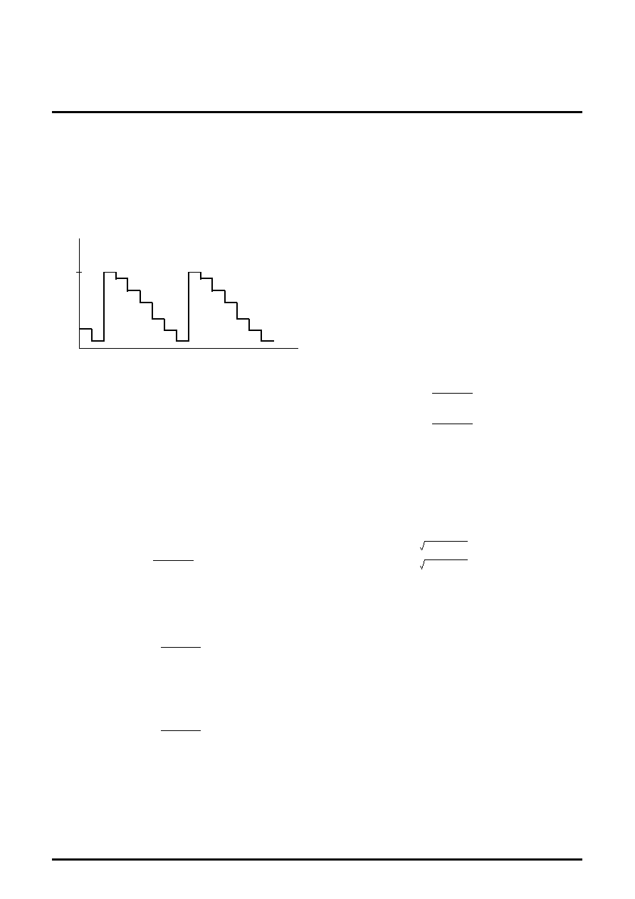
TP16 OUTPUT WAVEFORM
0.0
9.0
(V)
V
0
[V
P-P
]
0.7 [V
P-P
]
[dB]
G
V
=20LOG
V
01
[V
P-P
]
0.7 [V
P-P
]
[dB]
V
CR1
=20LOG
V
02
[V
P-P
]
0.7 [V
P-P
]
[dB]
V
CR2
=20LOG
V
02
[V
P-P
]
V
01
[V
P-P
]
[dB]
F
1-a
=20LOG
V
03
[V
P-P
]
V
01
[V
P-P
]
[dB]
F
2-a
=20LOG
T
r
(nsec)= (T
r2
)
2
-(T
r1
)
2
T
f
(nsec)= (T
f2
)
2
-(T
f1
)
2

MITSUBISHI ICs (Monitor)
M52721SP
WIDEBAND VIDEO PREAMPLIFIER WITH OSD MIX
4
INPUT SIGNAL
SG No.
Signals
SG1
Sine wave with amplitude 0.7V
P-P
(100kHz, amplitude partially variable
)
SG2
Sine wave with amplitude 0.7V
P-P
(f=100MHz)
SG3
Sine wave with amplitude 0.7V
P-P
(f=200MHz)
SG5
Pulse with amplitude 0.7V
P-P
(f=30kHz, duty=50%)
SG6
CP
+
Pulse with amplitude 4.0V
P-P
and pulse width 3.0
µ
s synchronous with the pedestal part of standard video stepped wave
(f=30kHz, pulse width and amplitude partially variable)
SG7
BLK,
OSD
signals
Pulse with amplitude 4.0V
P-P
and pulse width 10
µ
s synchronous with the image part of standard video stepped wave
(f=30kHz, amplitude partially variable
)
SG8
Standard
video
stepped
wave
Video signal with pulse width 0.7V
P-P
(f=30kHz, amplitude partially variable
)
0.7V
P-P
0.7V
P-P
4.0V
P-P
3.0
µ
s
0V
4.0V
P-P
10
µ
s
0V
V
20th
BLK input threshold voltage
Make sure that signal is not output in synchronization with SG7
(blanking portion).
Next, while monitoring this output, decrease the SG7 amplitude
gradually and measure the SG7 amplitude when the blanking
portion disappears.
O
aj1
OSD adjust control characteristics
1
Measure the amplitude of the output.
O
aj2
OSD adjust control characteristics
2
The conditions are the same as in O
aj1
above except that V18 is set
at 2V.