MITSUBISHI ICs (Monitor)
M52337SP
3-CHANNEL VIDEO PREAMPLIFIER WITH OSD MIXING FUNCTION
FOR HIGH-RESOLUTION COLOR DISPLAYS
1
DESCRIPTION
M52337SP is a video preamplifier provided with OSD mixing
function, and a semi-conductor IC having three channels of a built-
in amplifier in the 110MHz band.
Each channel has the functions of OSD blanking, OSD mixing,
wideband amplifier, main and sub-contrast control, and main and
sub brightness. Accordingly, it is structured to best fit the OSD-
provided high-resolution display.
FEATURES
·
Frequency band: RGB ...................................110MHz (at 3V
P-P
)
OSD......................................................50MHz
Input : RGB...........................................................0.7V
P-P
(Typ.)
OSD.............................3.0 to 5.0 V
P-P
(positive polarity)
BLK..........................4.0 V
P-P
or more (positive polarity)
Output : RGB........................................................4.0 V
P-P
(max.)
OSD..............................3.5 V
P-P
(max., black level=2V)
·
Each control of contrast and brightness includes a main which
allows three channels to be variable simultaneously, and a sub
which allows each channel to be variable independently. Each
control pin can be controlled within a range of 0 to 5V.
·
A built-in feedback circuit inside IC provides a stable DC level at
IC output pins.
·
Pin arrangement of M52337SP is the same as that of M52321SP.
APPLICATION
CRT display
RECOMMENDED OPERATING CONDITION
Supply voltage range...........................................Vcc=11.5 to 12.5V
Rated supply voltage........................................................Vcc=12.0V
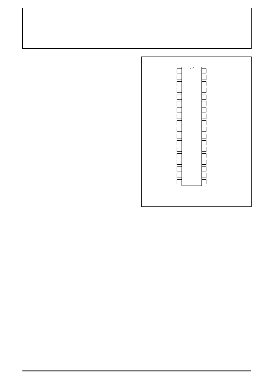
PIN CONFIGURATION (TOP VIEW)
Outline 36P4E
36
33
34
35
1
4
3
2
32
5
31
6
28
9
27
10
26
11
25
12
13
14
24
23
7
8
30
29
15
22
16
21
17
20
18
19
NC:NO CONNECTION
BLK IN
V
CC1
(B)
INPUT (B)
SUB CONTRSAST (B)
OSD IN (B)
GND 1 (B)
V
CC1
(G)
INPUT (G)
SUB CONTRST (G)
OSD IN (G)
GND 1 (G)
INPUT (R)
OSD ADJUST
OUTPUT (B)
V
CC2
(B)
HOLD (B)
SUB BRIGHTNESS (B)
V
CC2
(G)
OUTPUT (G)
GND2 (B)
HOLD (G)
SUB BRIGHTNESS (G)
GND2 (G)
OUTPUT (R)
V
SS2
(R)
HOLD (R)
M52337SP
SUB CONTRAST (R)
OSD IN (R)
GND 1 (R)
MAIN CONTRAST
CP IN
SUB BRIGHTNESS (R)
GND2 (B)
NC
MAIN BRIGHTNESS
V
CC1
(R)
MITSUBISHI ICs (Monitor)
M52337SP
3-CHANNEL VIDEO PREAMPLIFIER WITH OSD MIXING FUNCTION
FOR HIGH-RESOLUTION COLOR DISPLAYS
2
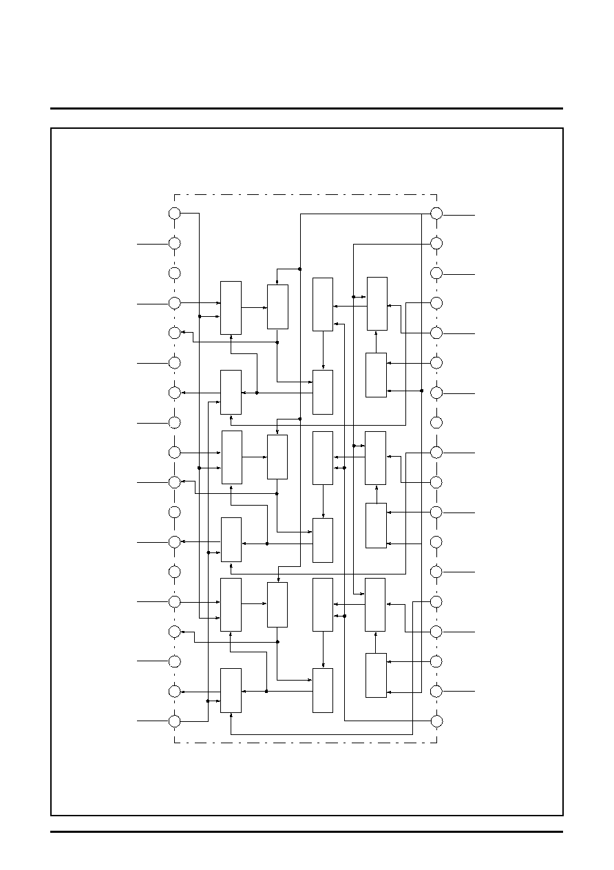
BLOCK DIAGRAM
(G)
OUTPUT
11
12
13
14
15
16
17
18
1
2
3
4
5
6
7
8
9
10
26
25
24
23
22
21
20
19
27
35
34
33
32
31
30
29
28
36
NC
(R) SUB
BRIGHTNESS
(R)
V
CC2
(G)
GND2
(R)
GND2
MAIN
BRIGHTNESS
(R)
HOLD
(R)
OUTPUT
(G)
HOLD
(G) SUB
BRIGHTNESS
(G)
V
CC2
(G)
GND2
(B) SUB
BRIGHTNESS
(B)
V
CC2
(B)
HOLD
(B)
OUTPUT
OSD
ADJUST
(G)
INPUT
CP IN
(R)
GND1
(R) SUB
CONTRAST
(R)
V
CC1
(G)
OSD IN
(B)
GND1
(B) SUB
NONTRAST
(B)
V
CC1
(R)
OSD IN
MAIN
CONTRAST
(R)
INPUT
(G)
GND1
(G) SUB
CONTRAST
(G)
V
CC1
(B)
OSD IN
(B)
INPUT
BLK
IN
B
OSD MIX
G
OSD MIX
R
OSD MIX
R
HOLD
B
HOLD
G
HOLD
B
AMP
R
AMP
G
AMP
R
CLAMP
G
CLAMP
B
CLAMP
B
BRIGHTNESS
G
BRIGHTNESS
R
BRIGHTNESS
B
BLANKING
G
BLANKING
R
BLANKING
B
CONTRAST
G
CONTRAST
R
CONTRAST

MITSUBISHI ICs (Monitor)
M52337SP
3-CHANNEL VIDEO PREAMPLIFIER WITH OSD MIXING FUNCTION
FOR HIGH-RESOLUTION COLOR DISPLAYS
3
ABSOLUTE MAXIMUM RATINGS (Ta=25°C)
ELECTRICAL CHARACTERISTICS
(Ta=25°C, Vcc=12V, unless otherwise noted)
Symbol
Parameter Ratings
Unit
Vcc
Supply voltage
13.0
V
P
d
Power dissipation
2016
mW
S
urge
Surge pressure
±
200
V
V
opr
Recommended supply voltage
12.0
V
V
opr'
Recommended supply voltage range
11.5 to12.5
V
T
opr
Operating temperature
-20 to +85
°C
T
stg
Storage temperature
-40 to +150
°C
Symbol
Parameter
Test
point
Input
External power supply(V)
Pulse input
Limits
Unit
SW13
R-ch
SW8
G-ch
SW13
B-ch
V4
V17
V19
V32
V36
SW18
SW1
5,10,15
Min. Typ. Max.
Icc
Circuit current
A
a
_
a
_
a
_
5
5
5
5
2
b
SG6
a
_
65
95
125
mA
Vomax
Output dynamic range
T.P35
T.P30
T.P25
b
SG1
b
SG1
b
SG1
5
5
Vari-
able
5
-
a
_
a
_
5.8
6.8
9.0
V
P-P
Vimax
Max. allowable input
T.P35
T.P30
T.P25
b
SG1
b
SG1
b
SG1
5
2.5
Vari-
able
5
-
a
_
a
_
1.7
2.4
2.9
V
P-P
Gv
Max. gain
T.P35
T.P30
T.P25
b
SG1
b
SG1
b
SG1
5
5
VT
5
-
a
_
a
_
13
17
20
dB
Gv
Relative max. gain
Take the ratio of the above values
0.8
1
1.2
-
V
CR1
Main contrast control character-
istics (at typ.)
T.P35
T.P30
T.P25
b
SG1
b
SG1
b
SG1
5
2
VT
5
-
a
_
a
_
5
8
11
dB
V
CR1
Relative main contrast control
characteristics (at typ.)
Take the ratio of the above values
0.8
1
1.2
-
V
CR2
Main contrast control character-
istics (at min.)
T.P35
T.P30
T.P25
b
SG1
b
SG1
b
SG1
5
1
VT
5
-
a
_
a
_
0.5
0.8
1.1
V
P-P
V
CR2
Relative main contrast control
characteristics (at min.)
Take the ratio of the above values
0.8
1
1.2
-
V
SCR1
Sub-contrast control character-
istics (at typ.)
T.P35
T.P30
T.P25
b
SG1
b
SG1
b
SG1
2
5
VT
5
-
a
_
a
_
5
8
11 dB
V
SCR1
Relative sub-contrast control
characteristics (at typ.)
Take the ratio of the above values
0.8
1
1.2
-
V
SCR2
Sub-contrast control character-
istics (at min.)
T.P35
T.P30
T.P25
b
SG1
b
SG1
b
SG1
1
5
VT
5
-
a
_
a
_
0.5
0.8
1.1
V
P-P
V
SCR2
Relative sub-contrast control
characteristics (at min.)
Take the ratio of the above values
0.8
1
1.2
-
V
SCR3
Main and sub brightness con-
trol characteristics (both main
and sub at typ.)
T.P35
T.P30
T.P25
b
SG1
b
SG1
b
SG1
3
3
VT
5
-
a
_
a
_
0.8
1.5
2.2
V
P-P
V
SCR3
Relative main and sub bright-
ness control characteristics
(both main and sub at typ.)
Take the ratio of the above values
0.8
1
1.2
-
V
B1
Main brightness control charac-
teristics (at max.)
T.P35
T.P30
T.P25
a
_
a
_
a
_
5
5
4
5
-
b
SG6
a
_
3.0
3.6
4.2
V
V
B1
Relative main brightness con-
trol characteristics (at max.)
Take the ratio of the above values
-0.3
0
0.3
V
V
B2
Main brightness control charac-
teristics (at typ.)
T.P35
T.P30
T.P25
a
_
a
_
a
_
5
5
2.5
5
-
b
SG6
a
_
1.6
2.2
2.8
V
V
B2
Relative main brightness con-
trol characteristics (at typ.)
Take the ratio of the above values
-0.3
0
0.3
V
V
B3
Main brightness control charac-
teristics (at min.)
T.P35
T.P30
T.P25
a
_
a
_
a
_
5
5
1
5
-
b
SG6
a
_
0.8
1.2
1.6
V
DC
V
B3
Relative main brightness con-
trol characteristics (at min.)
Take the ratio of the above values
-0.3
0
0.3
V

MITSUBISHI ICs (Monitor)
M52337SP
3-CHANNEL VIDEO PREAMPLIFIER WITH OSD MIXING FUNCTION
FOR HIGH-RESOLUTION COLOR DISPLAYS
4
ELECTRICAL CHARACTERISTICS
(cont.)
Symbol
Parameter
Test
point
Input
External power supply(V)
Pulse input
Limits
Unit
SW13
R-ch
SW8
G-ch
SW13
B-ch
V4
V17
V19
V32
V36
SW18
SW1
5,10,15
Min. Typ. Max.
V
SB1
Sub-brightness control charac-
teristics (at max.)
T.P35
T.P30
T.P25
a
_
a
_
a
_
5
5
2
5
-
b
SG6
a
_
1.3
1.8
2.4
V
DC
V
SB1
Sub-brightness control charac-
teristics (at min.)
T.P35
T.P30
T.P25
a
_
a
_
a
_
5
5
2
0
-
b
SG6
a
_
0.8
1.2
1.6
V
DC
F
C1
Frequency characteristics 1
(f=50MHz at max.)
T.P35
T.P30
T.P25
b
SG3
b
SG3
b
SG3
5
3
VT
-
-
a
_
a
_
-2.5
-1
3
dB
F
C1
Relative frequency characteris-
tics 1 (f=50MHz at max.)
Take the ratio of the above values
-1
0
1
dB
F
C1'
Frequency characteristics 1
(f=110MHz at max.)
T.P35
T.P30
T.P25
b
SG4
b
SG4
b
SG4
5
3
VT
-
-
a
_
a
_
-3
-2
3
dB
F
C1'
Relative frequency characteris-
tics (f=110MHz at max.)
Take the ratio of the above values
-2
0
2
dB
F
C2
Frequency characteristics 2
(f=110MHz at typ.)
T.P35
T.P30
T.P25
b
SG3
b
SG3
b
SG3
5
2
VT
-
-
a
_
a
_
-3
-2
3
dB
V
C2'
Relative frequency characteris-
tics 2 (f=110MHz at typ.)
T.P35
T.P30
T.P25
b
SG4
b
SG4
b
SG4
5
2
VT
-
-
a
_
a
_
-2
0
2
dB
F
C3
Frequency characteristics 3
(f=110MHz at min.)
T.P35
T.P30
T.P25
b
SG3
b
SG3
b
SG3
5
1
VT
-
-
a
_
a
_
-3
-2
3
dB
F
C3'
Relative frequency characteris-
tics 3 (f=110MHz at min.)
T.P35
T.P30
T.P25
b
SG4
b
SG4
b
SG4
5
1
VT
-
-
a
_
a
_
-2
0
2
dB
C.T.1
Crosstalk1(f=50MHz )
T.P35
T.P30
T.P25
b
SG3
a
_
a
_
5
5
VT
5
-
a
_
a
_
-
-30
-20
dB
C.T.1'
Crosstalk1(f=110MHz )
T.P35
T.P30
T.P25
b
SG4
a
_
a
_
5
5
VT
5
-
a
_
a
_
-
-20
-15
dB
C.T.2
Crosstalk2(f=50MHz )
T.P35
T.P30
T.P25
a
_
b
SG3
a
_
5
5
VT
5
-
a
_
a
_
-
-30
-20
dB
C.T.2'
Crosstalk2(f=110MHz )
T.P35
T.P30
T.P25
a
_
b
SG4
a
_
5
5
VT
5
-
a
_
a
_
-
-20
-15
dB
C.T.3
Crosstalk3(f=50MHz )
T.P35
T.P30
T.P25
a
_
a
_
b
SG3
5
5
VT
5
-
a
_
a
_
-
-30
-20
dB
C.T.3'
Crosstalk2(f=110MHz )
T.P35
T.P30
T.P25
a
_
a
_
b
SG4
5
5
VT
5
-
a
_
a
_
-
-20
-15
dB
Tr
Pulse characteristics 1
T.P35
T.P30
T.P25
b
SG5
b
SG5
b
SG5
5
3.3
2
5
-
b
SG6
a
_
-
4
7
nsec
Tf
Pulse characteristics 2
T.P35
T.P30
T.P25
b
SG5
b
SG5
b
SG5
5
3.3
2
5
-
b
SG6
a
_
-
7
9
nsec
V14th
Clamping pulse threshold volt-
age
T.P35
T.P30
T.P25
a
_
a
_
a
_
5
5
2
5
-
b
SG6
a
_
0.7
1.5
2.5
V
DC
W14
Clamping pulse min. operating
width
T.P35
T.P30
T.P25
a
_
a
_
a
_
5
5
2
5
-
b
SG6
a
_
-
0.3
1.0
µ
sec
OTr
OSD pulse characteristics 1
T.P35
T.P30
T.P25
a
_
a
_
a
_
5
5
2
5
4.5
b
SG6
b
SG8
-
5
10
nsec
OTf
OSD pulse characteristics 2
T.P35
T.P30
T.P25
a
_
a
_
a
_
5
5
2
5
4.5
b
SG6
b
SG8
-
5
10
nsec
Oaj1
OSD adjustment control char-
acteristics (at max.)
T.P35
T.P30
T.P25
a
_
a
_
a
_
5
5
2
5
4.5
b
SG6
b
SG8
2.5
3.1
3.6
V
P-P
Oaj1
Relative OSD adjustment con-
trol characteristics (at max.)
Take the ratio of the above values
0.8
1
1.2
-
Oaj2
OSD adjustment Control char-
acteristics (at min.)
T.P35
T.P30
T.P25
a
_
a
_
a
_
5
5
2
5
0
b
SG6
b
SG8
-0.5
0
0.5
V
P-P
Oaj2
Relative OSD adjustment Con-
trol characteristics (at min.)
Take the ratio of the above values
0.8
1
1.2
-
MITSUBISHI ICs (Monitor)
M52337SP
3-CHANNEL VIDEO PREAMPLIFIER WITH OSD MIXING FUNCTION
FOR HIGH-RESOLUTION COLOR DISPLAYS
5
ELECTRICAL CHARACTERISTICS
(cont.)
Symbol
Parameter
Test
point
Input
External power supply(V)
Pulse input
Limits
Unit
SW13
R-ch
SW8
G-ch
SW13
B-ch
V4
V17
V19
V32
V36
SW18
SW1
5,10,15
Min. Typ. Max.
OSDth
OSD input threshold voltage
T.P35
T.P30
T.P25
a
_
a
_
a
_
5
5
2
5
1.7
b
SG6
b
SG8
1.7
2.5
3.5
V
DC
V1th
BLK input threshold voltage
T.P35
T.P30
T.P25
b
SG7
b
SG7
b
SG7
5
5
2
5
-
b
SG6
SW1 only
b
SG8
1.7
2.5
3.5
V
DC
ELECTRICAL CHARACTERISTICS TEST METHOD
SW/NO of signal input pin and SW/NO of pulse input pin, which
have already been described in the electrical characteristics table,
are omitted, and SW/NO of external power supply will only be
described as follows:
Sub-brightness voltages, V32, V27 and V22, which are always set
to the identical value, are represented by V32 in the electrical
characteristic table. In addition, sub-contract voltages, V4, V9 and
V14, which are also set to the identical value, are represented by V4
in the table.
Icc circuit current
Conditions shall be as specified in the electrical characteristic table,
and take measurements with ammeter A when SW1 is turned to the
b side.
Vomax output dynamic range
Follow the following procedure to set V19.
1. Input SG1 to pin
(pin
or pin
), gradually raise V19, and
read V19 voltage when the upper part of the output waveform of
T.P25 (T.P30 or T.P35) is distorted to let the reading be VTR1
(V
TG
1 or V
TB
1).
In addition, gradually reduce V19 conversely, and read V19
voltage when the lower part of the output waveform of T.P35
(T.P30 or T.P25) is distorted to let the reading be V
TR
2 (V
TG
2 or
V
TB
2).
2. From the above, V
T
(V
TR
, V
TG
or V
TB
) is found by
which should be used properly depending upon output pins.
In measuring, use
3. After setting V
TR
(V
TG
or V
TB
), gradually increase SG1 amplitude
from 700mV, and take measurements of output amplitude at a
point where the upper and lower parts of T.P25 (T.P30 or T.P35)
output waveform start to be distorted simultaneously.
Vimax max. allowable input
From the status of Vomax, change V17 into 2.5V as specified in the
electrical characteristics table, gradually increase input signal
amplitude from 700m V
P-P
, and read input signal amplitude at a
point where output signal starts to be distorted.
GV and
GV max gain and relative max. gain
1. Input SG1 to pin
(pin
or pin
), read the output amplitude
of T.P25 (T.P30 or T.P35) to let the reading be V
OR1
(V
OG1
or
V
OB1
).
2. Max. gain GV is found by:
3. Relative max. gain
G is found by
G
V
=V
OR1
/V
OG1
, V
OG1
/V
OB1
, V
OB1
/
VOR1
through respective calculation.
V
CR1
main contrast control characteristics (at typ.) and
V
CR1
relative main contrast control characteristics (at typ.)
1. Follow the electrical characteristic table except changing V17 to
2.0V.
2. Read the output amplitude of T.P25 (T.P30 or T.P35) at this time
to let the reading be V
OR2
(V
OG2
or V
OB2
).
3. Contrast control characteristics V
CR1
and relative contrast control
characteristics
V
CR1
are found by
through respective calculation.
V
CR2
main contrast control characteristics (at min.) and
V
CR2
relative main contrast control characteristics (at min.)
1. Follow the electrical characteristic table except changing V17 to
1.0V.
2. Read the output amplitude of T.P25 (T.SP30 or T.P35) to let the
reading be V
OR3
(V
OG3
or V
OG3
) to let it be V
CR2
, respective
3. Relative contrast control characteristic
V
CR2
is found by:
V
CR2
=V
OR3
/V
OG3
, V
OG3
/V
OB3
, V
OB3
/V
OR3
13
8
3
(V)
5.0
0.0
Output waveform of T.P25 (T.P30 and T.P35 are also the same)
V
TR
(V
TG
, V
TB
)=
V
TR1
(V
TG1
, V
TB1
)+V
TR2
(V
TG1
, V
TB1
)
2
T.P25 V
TR1
,T.P30 V
TG1
and T.P35 V
TB1
.
13
8
3
G
V
=20log
V
OR1
(V
OG1
, V
OB1
) [V
P-P
]
0.7 [V
P-P
]
V
OR1
=V
CR2
/V
OG2
, V
OG2
/V
OB2
, V
OB2
/V
OR2
V
CR1
=20log
V
OR2
(V
OG2
, V
OB2
) [V
P-P
]
0.7 [V
P-P
]