2835X-DSH-001-D
Mindspeed TechnologiesTM
May 2003
Preliminary Information/Mindspeed Proprietary and Confidential
M28352/M28353/M28354/M28356 (M2835x)
Dual/Triple/Quad/Hex DS3/E3/STS-1 Line Interface Unit with Integrated DJAT
Preliminary Information
This document contains information on a new product. The parametric information, although not
fully characterized, is the result of testing initial devices.
J A T
E n c o d e r
A M I/E 3
G e n
&
P u ls e
S h a p e r
R P O S n
T P O S n
T N E G n
T C L K n
R X _ L IN E P _ n
L in e
D r iv e r
T X _ L I N E P _ n
T X _ L I N E M _ n
R C L K n
R N E G n
P R B S
P a t t e r n
G e n /D e t
D e c o d e r
C D R
Digital
Adaptor
Equalizer
R L O S
R X _ L IN E M _ n
R L O S n
L IU a n d J A T 1 t o 5
L IU a n d J A T 0
R e c e iv e r
S T S 1 _ R E F C L K
D S 3 _ R E F C L K
E 3 _ R E F C L K
C L K 1 9 P 4 4 _ IO
C L A D s
X T A L _ IN
A D D R n /L L O O P n /R L O O P n
T A IS n
Co
nt
r
o
l
R E S E T B
IR Q B
IF _ M O D E 0
IF _ M O D E 1
S C L K
O E B
S D IN
S D O U T
C S B
D A T A n /L B O n /R L O O P n
R W B
L IN E R A T E 0
E N n
L IU _ B Y P
J A T R X
L IN E R A T E 1
.
.
.
JT
A
G
T R S T
T C L K
T D I
T M S
T D O
S C A N M O D E
P R B S
P a t t e r n
G e n /D e t
T L O S
T L O S n
M O N
L o g ic
M O N _ O P
M O N _ O M
M O N _ IN M
M O N _ IN P
X T A L _ O U T
Applications
Multi-service ATM switches
Optical add-drop multiplexers
Digital cross-connect systems (DACS)
DS3 to STS-1 mappers
E3 to STS-1 mappers
High-end routers
Metro-optical access switches
Standards Compliant--Complies with all applicable
DS3/E3/STS-1 standards:
Telcordia GR-253, GR-499
ETSI TBR-24 and ETS 300
ANSI T1.102, T1.105.03b, T1.404
ITU-T G.703, G.751, G.755, G.783, G.823, G.824, 0.151
AT&T TR54014
Functional Block Diagram
Distinguishing Features
Highly Integrated--Up to six independently configured LIUs with
jitter attenuator/desynchronizer channels for DS3, E3 and STS-1
applications
LIUs with Desynchronizers--For Category I interfaces, smoothes the
jitter due to the demapping, bit stuffing, and pointer adjustments in
the DS3 or E3 payloads extracted from the STS-1 frames, generating
a standards compliant clock.
LIUs with Jitter Attenuators--For Category II interfaces, the device
synchronizes to jittered DS3, E3 or STS-1 clock and data input
signals and produces a de-jittered standards compliant clock and
data output.
LIUs with Adaptive Equalization--Automatic adaptive equalization up
to 1,800 feet for AT&T 734/728 75 ohm type cables
Internally Synthesized Clocks--Three Clock Rate Adaptors (CLADs)
providing DS3, E3 and/or STS-1 clock rates from a single 19.44 MHz
crystal or external input.
(continued on page iii)
The M28352/M28353/M28354/M28356 (M2835x) is a 2/3/4/6-port Line Interface Unit (LIU) and Desynchronizer/Jitter
Attenuator (DJAT) for DS3, E3, and STS-1 applications. This highly-integrated, multi-channel, low power solution is capable
of receiving data over 1800 feet of AT&T 734/728 75 ohm type cables and provide standards compliant smooth/de-jittered
clock and data to the system.
The M2835x includes diagnostics and quality monitoring functions for the detection of system and board level operating
conditions and failures. The device provides the capability to monitor RLOS and RLOS integration per GR-253, transmit
loss of signal, transmit open circuits, receiver line input opens and shorts, and clock quality and it includes a clock offset
indicator. Diagnostics capabilities include Fixed and PRBS pattern generation/detection, single error insertion and
detection, bit and error counters to support Bit Error Rate calculations, and full loopback capabilities.
Each M2835x channel can be independently configured for DS3, E3, or STS-1 applications as a LIU with desynchronizer,
LIU with jitter attenuator, or LIU with DJAT disabled or powered down. Each channel can be independently powered down
for low power operation.
ˋ 2002, 2003,
Mindspeed TechnologiesTM, A Conexant Business
All rights reserved.
Information in this document is provided in connection with Mindspeed Technologies ("Mindspeed") products. These materials are provided by
Mindspeed as a service to its customers and may be used for informational purposes only. Mindspeed assumes no responsibility for errors or
omissions in these materials. Mindspeed may make changes to specifications and product descriptions at any time, without notice. Mindspeed
makes no commitment to update the information and shall have no responsibility whatsoever for conflicts or incompatibilities arising from future
changes to its specifications and product descriptions.
No license, express or implied, by estoppel or otherwise, to any intellectual property rights is granted by this document. Except as provided in
Mindspeed's Terms and Conditions of Sale for such products, Mindspeed assumes no liability whatsoever.
THESE MATERIALS ARE PROVIDED "AS IS" WITHOUT WARRANTY OF ANY KIND, EITHER EXPRESS OR IMPLIED, RELATING TO SALE
AND/OR USE OF MINDSPEED PRODUCTS INCLUDING LIABILITY OR WARRANTIES RELATING TO FITNESS FOR A PARTICULAR
PURPOSE, CONSEQUENTIAL OR INCIDENTAL DAMAGES, MERCHANTABILITY, OR INFRINGEMENT OF ANY PATENT, COPYRIGHT OR
OTHER INTELLECTUAL PROPERTY RIGHT. MINDSPEED FURTHER DOES NOT WARRANT THE ACCURACY OR COMPLETENESS OF
THE INFORMATION, TEXT, GRAPHICS OR OTHER ITEMS CONTAINED WITHIN THESE MATERIALS. MINDSPEED SHALL NOT BE
LIABLE FOR ANY SPECIAL, INDIRECT, INCIDENTAL, OR CONSEQUENTIAL DAMAGES, INCLUDING WITHOUT LIMITATION, LOST
REVENUES OR LOST PROFITS, WHICH MAY RESULT FROM THE USE OF THESE MATERIALS.
Mindspeed products are not intended for use in medical, lifesaving or life sustaining applications. Mindspeed customers using or selling
Mindspeed products for use in such applications do so at their own risk and agree to fully indemnify Mindspeed for any damages resulting from
such improper use or sale.
The following are trademarks of Conexant Systems, Inc.: Mindspeed TechnologiesTM, the MindspeedTM logo, and "Build It First"TM. Product
names or services listed in this publication are for identification purposes only, and may be trademarks of third parties. Third-party brands and
names are the property of their respective owners.
For additional disclaimer information, please consult Mindspeed Technologies Legal Information posted at
www.mindspeed.com
which is
incorporated by reference.
2835X-DSH-001-D
Mindspeed TechnologiesTM
ii
Preliminary Information/Mindspeed Proprietary and Confidential
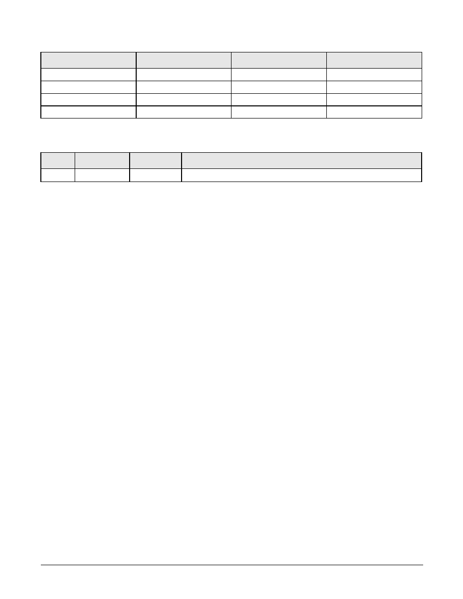
Ordering Information
Model Number
Number of Channels
Package
Operating Temperature
M28352
2
280-ball 19 mm FPBGA
Ù40
¯
C to 85
¯
C
M28353
3
280-ball 19 mm FPBGA
Ù40
¯
C to 85
¯
C
M28354
4
280-ball 19 mm FPBGA
Ù40
¯
C to 85
¯
C
M28356
6
452-ball 27 mm PBGA
Ù40
¯
C to 85
¯
C
Revision History
Revision
Level
Date
Description
D
Preliminary
May 2003
Changed external reference clock accuracy to +/- 20 ppm.

2835X-DSH-001-D
Mindspeed TechnologiesTM
iii
Preliminary Information/Mindspeed Proprietary and Confidential
M28352/M28353/M28354/M28356 (M2835x) Data Sheet
Distinguishing Features
(continued from front page)
Three Interfaces for Configuration:
Hardware interface pins
Serial microprocessor interface port
Parallel microprocessor interface
port
Qualify Monitoring
Determines the integrity of the
signals
Continuously monitor the quality of
the connections
RLOS receive loss of signal indicator
circuit compliant with ITU-T G.775
TLOS internal or external transmit
loss of signal indication
DC continuity check of receive input
ITU-T G.772-compliant monitoring
circuit that monitors the performance
of transmit signals
Clock meter indicates the quality of
recovered receive clocks used to alert
network operators of variations in the
network
Alarm Indication Signal--TAIS alarm
indication signal for DS3 AIS and E3 AIS
Suppression Encoding Error Counters
Line Code Violation (LCV) Counter
Bipolar Violation (BPV) Counter
Excessive Zeros (EXZ) Counter
Event Latching--One-second timer for
event latching of counters
Diagnostics, Per Channel:
PRBS detection and/or generation
3-bit Fixed Pattern detection and/or
generation (B3ZS testing)
4-bit Fixed Pattern detection and/or
generation (HDB3 testing)
Single error insertion into generated
pattern
Single bit error detection and
counting
Received bit counting to support Bit
Error Rate calculations
Loopbacks, Per Channel:
Line loopback
Analog loopback (analog line receive
data looped back to analog transmit
data)
Source loopback
JTAG Interface--JTAG (IEEE 1149.1)
boundary scan
Seamless Framer Interface --Interfaces
seamlessly with other components in
Mindspeed's DS3/E3 family of devices
such as CX28365 and CX2834x
(multiport) DS3/E3 framers.
Operating Conditions
Uses 3.3 V and 1.8 V supplies
Operates from Ù40
¯
C to 85
¯
C
Power Consumption
Independent channel power-down
control for low power operation
Size
6-port device in a 27 mm PBGA package
2, 3, and 4-port devices in a 19 mm
FPBGA package

2835X-DSH-001-D
Mindspeed TechnologiesTM
v
Preliminary Information/Mindspeed Proprietary and Confidential
Contents
Contents
. . . . . . . . . . . . . . . . . . . . . . . . . . . . . . . . . . . . . . . . . . . . . . . . . . . . . . . . . v
Figures
. . . . . . . . . . . . . . . . . . . . . . . . . . . . . . . . . . . . . . . . . . . . . . . . . . . . . . . . . xi
Tables
. . . . . . . . . . . . . . . . . . . . . . . . . . . . . . . . . . . . . . . . . . . . . . . . . . . . . . . . xiii
1.0 Product Description. . . . . . . . . . . . . . . . . . . . . . . . . . . . . . . . . . . . . . . . . . . . . . 1-1
1.1
Overview . . . . . . . . . . . . . . . . . . . . . . . . . . . . . . . . . . . . . . . . . . . . . . . . . . . . . . . . . . . . . . . . . . . . . . . 1-1
1.2
Pin Diagrams. . . . . . . . . . . . . . . . . . . . . . . . . . . . . . . . . . . . . . . . . . . . . . . . . . . . . . . . . . . . . . . . . . . . 1-2
1.2.1
M28356. . . . . . . . . . . . . . . . . . . . . . . . . . . . . . . . . . . . . . . . . . . . . . . . . . . . . . . . . . . . . . . . . . 1-2
1.2.2
M28354. . . . . . . . . . . . . . . . . . . . . . . . . . . . . . . . . . . . . . . . . . . . . . . . . . . . . . . . . . . . . . . . . . 1-4
1.2.3
M28353. . . . . . . . . . . . . . . . . . . . . . . . . . . . . . . . . . . . . . . . . . . . . . . . . . . . . . . . . . . . . . . . . . 1-6
1.2.4
M28352. . . . . . . . . . . . . . . . . . . . . . . . . . . . . . . . . . . . . . . . . . . . . . . . . . . . . . . . . . . . . . . . . . 1-8
1.3
Pin Definitions . . . . . . . . . . . . . . . . . . . . . . . . . . . . . . . . . . . . . . . . . . . . . . . . . . . . . . . . . . . . . . . . . . 1-10
2.0 Functional Description. . . . . . . . . . . . . . . . . . . . . . . . . . . . . . . . . . . . . . . . . . . . 2-1
2.1
Overview . . . . . . . . . . . . . . . . . . . . . . . . . . . . . . . . . . . . . . . . . . . . . . . . . . . . . . . . . . . . . . . . . . . . . . . 2-1
2.2
Clock Rate Adaptor Ù CLAD . . . . . . . . . . . . . . . . . . . . . . . . . . . . . . . . . . . . . . . . . . . . . . . . . . . . . . . . . 2-3
2.2.1
Overview . . . . . . . . . . . . . . . . . . . . . . . . . . . . . . . . . . . . . . . . . . . . . . . . . . . . . . . . . . . . . . . . . 2-3
2.2.2
Crystal Oscillator Circuitry Enabled . . . . . . . . . . . . . . . . . . . . . . . . . . . . . . . . . . . . . . . . . . . . . 2-4
2.2.2.1
Crystal Oscillator Circuitry Not Bypassed and the CLADs Enabled . . . . . . . . . . . . 2-4
2.2.2.2
Crystal Oscillator Circuitry Not Bypassed and the CLADs Disabled . . . . . . . . . . . . 2-5
2.2.3
Crystal Oscillator Circuitry Disabled . . . . . . . . . . . . . . . . . . . . . . . . . . . . . . . . . . . . . . . . . . . . 2-6
2.2.3.1
Crystal Oscillator Circuitry Bypassed and the CLADs Enabled. . . . . . . . . . . . . . . . 2-6
2.2.3.2
Crystal Oscillator Circuitry Bypassed and the CLADs Disabled . . . . . . . . . . . . . . . 2-7
2.3
Line Interface Unit Ù LIU . . . . . . . . . . . . . . . . . . . . . . . . . . . . . . . . . . . . . . . . . . . . . . . . . . . . . . . . . . . 2-7
2.3.1
Overview . . . . . . . . . . . . . . . . . . . . . . . . . . . . . . . . . . . . . . . . . . . . . . . . . . . . . . . . . . . . . . . . . 2-7
2.3.2
Transmitter . . . . . . . . . . . . . . . . . . . . . . . . . . . . . . . . . . . . . . . . . . . . . . . . . . . . . . . . . . . . . . . 2-8
2.3.2.1
AMI/B3ZS/HBD3 Encoder . . . . . . . . . . . . . . . . . . . . . . . . . . . . . . . . . . . . . . . . . . . 2-8
2.3.2.2
Pulse Shaper . . . . . . . . . . . . . . . . . . . . . . . . . . . . . . . . . . . . . . . . . . . . . . . . . . . . . 2-9
2.3.2.3
Line Driver . . . . . . . . . . . . . . . . . . . . . . . . . . . . . . . . . . . . . . . . . . . . . . . . . . . . . . 2-9
2.3.2.4
Transmit Monitor. . . . . . . . . . . . . . . . . . . . . . . . . . . . . . . . . . . . . . . . . . . . . . . . . 2-13
2.3.2.5
Alarm Indication Signal Generator Ù AIS . . . . . . . . . . . . . . . . . . . . . . . . . . . . . . . 2-16
2.3.3
Receiver . . . . . . . . . . . . . . . . . . . . . . . . . . . . . . . . . . . . . . . . . . . . . . . . . . . . . . . . . . . . . . . . 2-17
2.3.3.1
Overview . . . . . . . . . . . . . . . . . . . . . . . . . . . . . . . . . . . . . . . . . . . . . . . . . . . . . . . 2-17
2.3.3.2
AGC/VGA Block . . . . . . . . . . . . . . . . . . . . . . . . . . . . . . . . . . . . . . . . . . . . . . . . . . 2-17
2.3.3.3
Receive Equalizer . . . . . . . . . . . . . . . . . . . . . . . . . . . . . . . . . . . . . . . . . . . . . . . . 2-18
2.3.3.4
PLL Clock Recovery . . . . . . . . . . . . . . . . . . . . . . . . . . . . . . . . . . . . . . . . . . . . . . 2-18