Data Sheet
Mindspeed TechnologiesTM
500028C
Preliminary Information/Mindspeed Proprietary and Confidential
May 2002
CX28365/6/4
x12, x6, x4 T3/E3 Framer and ATM Cell
Transmission Convergence Sublayer
Processor
The CX2836x is a family of devices that provides up to twelve T3/E3 framers that
support DS3-M13, DS3-C-bit parity, E3-G.751, and E3-G.832 transmission formats
integrated with ATM physical layer processing functions. These functions are found
in the ATM Forum Cell-Based Transmission Convergence Sublayer Specification (af-phy-
0043.000), DS3 Physical Layer Interface S
pecification
(af-phy-0054.000), and
E3
Public
UNI S
pecification
(af-phy-0034.000).
The CX2836x provides framing recovery for M13, M23, C-bit parity, G.751, and
G.832 formatted signals. Access is provided to the FEAC and TDL channels.
The CX2836x device allows for ease of configuration, while providing maximum
flexibility to support the transmission and recovery of industry standard formats. It
provides a flexible opportunity bit generation method to source opportunity bits on
an individual framer.
The CX2836x provides a high-density and low-cost solution for T3 and E3 UNI
and NNI ATM interfaces. A complete design for interfacing cells from a standard
UTOPIA Level 2 system interface to the physical line connections requires only the
addition of four triple Line Interface Units (LIUs) or a single twelve port LIU, and a
microprocessor for configuration and control.
The CX28365 is an x12 T3/E3 framer with transmission convergence. The CX28366
is an x6 T3/E3 framer with transmission convergence, and the CX28364 is a quad T3/
E3 framer with transmission convergence. Both the CX28366 and CX28364 perform
identically to the CX28365.
Preliminary Information
This document contains information on a new product. The parametric information, although not
fully characterized, is the result of testing initial devices.
Distinguishing Features
Twelve, six, or four independent DS3/E3
framers in one package
Line coding supported:
DS3: B3ZS, NRZ, AMI
E3: HDB3, NRZ, AMI
Framing supported:
DS3: M13, M23, C-bit parity
E3: G.751, G.832
Inserts and extracts opportunity bits
Full FEAC and TDL channel support
Full performance monitoring support per
T1.231 standard
Glueless interfaces to the following
devices:
LIU Interfaces:
Mindspeed's DS3/E3/STS-1 LIU
CX283331x, 3x, M28335
SAR interfaces: Bt8233/RS8234
Network processors: CX27440/
CX27460
HDLC controllers: CX23500
S-RAM-type processor interface
PLCP or direct framing selectable
per port
Power supplies and power consumption
I/O 3.3 V, input 5 V tolerant, core 1.8 V
Low power operation (<190 mW per
port)
UTOPIA Interface
Level 2
8- and 16-bit modes
Multi-PHY capability
Redundant channel
Cell Delineator
Passes or rejects idle cells or selected
cells based on header register
configuration
Recovers cell alignment from HEC
Performs single-bit HEC error
correction and multiple-bit detection
Generates cell status bits, cell counts,
and error counts
Reads cell data from the UTOPIA FIFO
Inserts idle cells when no traffic is
available
ITU I.432-compliant
Testing
JTAG boundary scan support
Applications
Digital Cross-Connect Systems
Optical Transport Equipment
Access Concentrators
ATM Switches
Concentrators
Routers

© 2002,
Mindspeed TechnologiesTM, A Conexant Business
All rights reserved.
Information in this document is provided in connection with Mindspeed Technologies ("Mindspeed") products. These materials are provided by
Mindspeed as a service to its customers and may be used for informational purposes only. Mindspeed assumes no responsibility for errors or
omissions in these materials. Mindspeed may make changes to specifications and product descriptions at any time, without notice. Mindspeed
makes no commitment to update the information and shall have no responsibility whatsoever for conflicts or incompatibilities arising from future
changes to its specifications and product descriptions.
No license, express or implied, by estoppel or otherwise, to any intellectual property rights is granted by this document. Except as provided in
Mindspeed's Terms and Conditions of Sale for such products, Mindspeed assumes no liability whatsoever.
THESE MATERIALS ARE PROVIDED "AS IS" WITHOUT WARRANTY OF ANY KIND, EITHER EXPRESS OR IMPLIED, RELATING TO SALE
AND/OR USE OF MINDSPEED PRODUCTS INCLUDING LIABILITY OR WARRANTIES RELATING TO FITNESS FOR A PARTICULAR
PURPOSE, CONSEQUENTIAL OR INCIDENTAL DAMAGES, MERCHANTABILITY, OR INFRINGEMENT OF ANY PATENT, COPYRIGHT OR
OTHER INTELLECTUAL PROPERTY RIGHT. MINDSPEED FURTHER DOES NOT WARRANT THE ACCURACY OR COMPLETENESS OF
THE INFORMATION, TEXT, GRAPHICS OR OTHER ITEMS CONTAINED WITHIN THESE MATERIALS. MINDSPEED SHALL NOT BE
LIABLE FOR ANY SPECIAL, INDIRECT, INCIDENTAL, OR CONSEQUENTIAL DAMAGES, INCLUDING WITHOUT LIMITATION, LOST
REVENUES OR LOST PROFITS, WHICH MAY RESULT FROM THE USE OF THESE MATERIALS.
Mindspeed products are not intended for use in medical, lifesaving or life sustaining applications. Mindspeed customers using or selling
Mindspeed products for use in such applications do so at their own risk and agree to fully indemnify Mindspeed for any damages resulting from
such improper use or sale.
The following are trademarks of Conexant Systems, Inc.: Mindspeed TechnologiesTM, the MindspeedTM logo, and "Build It First"TM. Product
names or services listed in this publication are for identification purposes only, and may be trademarks of third parties. Third-party brands and
names are the property of their respective owners.
For additional disclaimer information, please consult Mindspeed Technologies Legal Information posted at
www.mindspeed.com
which is
incorporated by reference.
ii
Mindspeed TechnologiesTM
500028C
Preliminary Information/Mindspeed Proprietary and Confidential
Ordering Information
Model Number
Number of Framers
Package
Ambient Temperature Range
CX28365
12
456-ball, 35 mm PBGA
40
°
C to 85
°
C
CX28366
6
456-ball, 35 mm PBGA
40
°
C to 85
°
C
CX28364
4
456-ball, 35 mm PBGA
40
°
C to 85
°
C
Revision History
Revision
Level
Date
Description
101104
A
Advance
August 2000
Initial release.
101104
B
Advance
February 2001
Added timing diagrams, tables, and functional description. General
corrections. Deleted MDtack*.
101104C
Advance
February 2001
Added CX28366 and CX28364 versions. General corrections.
500028A
Advance
February 2001
Initial release under document number 500028A. Formerly document number
101104C.
500028
B
Advance
February 2002
Incorporated changes from Errata document 500152B dated 12/13/01 and
made general corrections.
500028C
Preliminary
May 2002
Incorporated Errata 500354A.

500028C
Mindspeed TechnologiesTM
v
Preliminary Information/Mindspeed Proprietary and Confidential
Contents
Figures
. . . . . . . . . . . . . . . . . . . . . . . . . . . . . . . . . . . . . . . . . . . . . . . . . . . . . . . . . xi
Tables
. . . . . . . . . . . . . . . . . . . . . . . . . . . . . . . . . . . . . . . . . . . . . . . . . . . . . . . . xiii
CHAPTER
1.0 Product Description. . . . . . . . . . . . . . . . . . . . . . . . . . . . . . . . . . . . . . . . . . . . . . 1-1
1.1
Application Overview . . . . . . . . . . . . . . . . . . . . . . . . . . . . . . . . . . . . . . . . . . . . . . . . . . . . . . . . . . . . . . 1-2
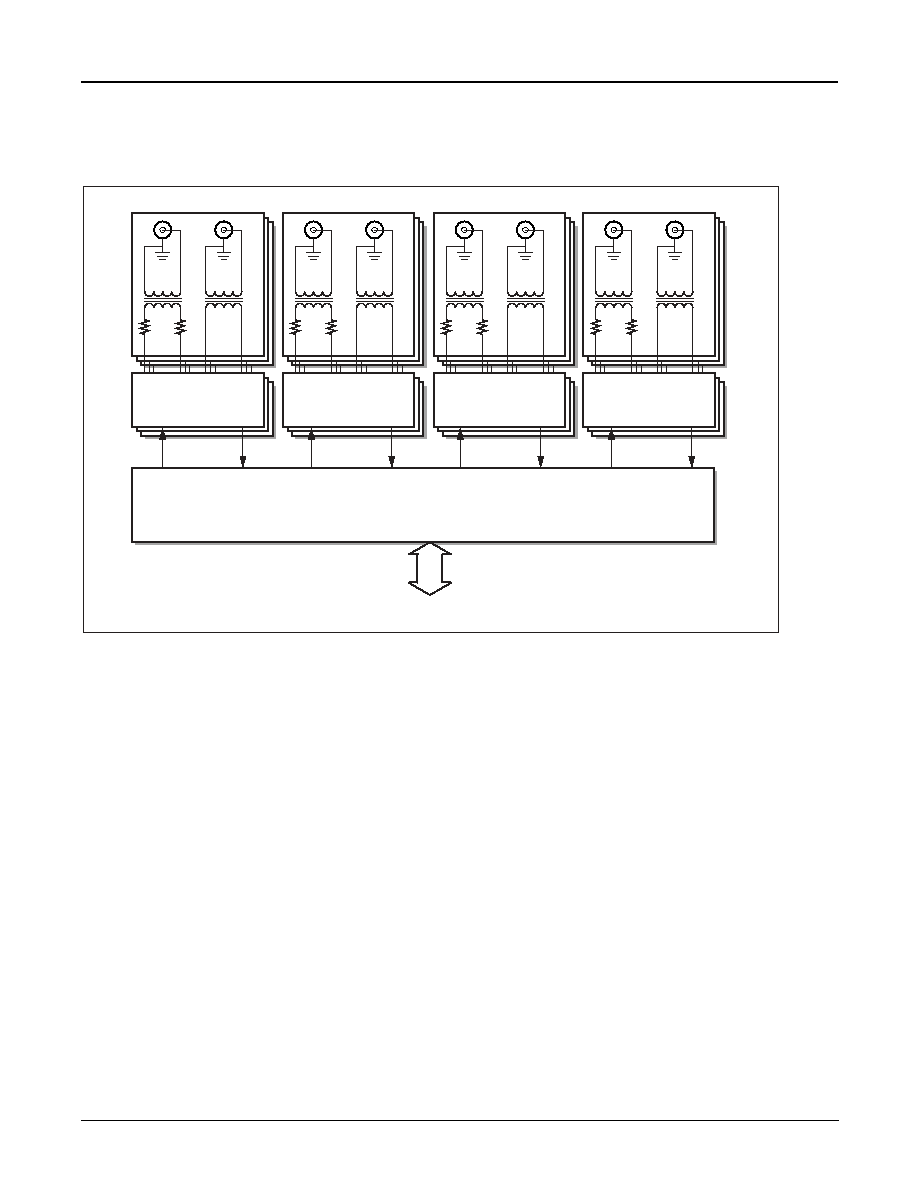
1.1.1
Logic Diagram. . . . . . . . . . . . . . . . . . . . . . . . . . . . . . . . . . . . . . . . . . . . . . . . . . . . . . . . . . . . . 1-2
1.2
Pin Diagram and Definitions . . . . . . . . . . . . . . . . . . . . . . . . . . . . . . . . . . . . . . . . . . . . . . . . . . . . . . . . 1-5
1.2.1
Pin Definitions. . . . . . . . . . . . . . . . . . . . . . . . . . . . . . . . . . . . . . . . . . . . . . . . . . . . . . . . . . . . . 1-9
2.0 Functional Description. . . . . . . . . . . . . . . . . . . . . . . . . . . . . . . . . . . . . . . . . . . . 2-1
2.1
T3/E3 Framer. . . . . . . . . . . . . . . . . . . . . . . . . . . . . . . . . . . . . . . . . . . . . . . . . . . . . . . . . . . . . . . . . . . . 2-3
2.1.1
Transmitter Operation . . . . . . . . . . . . . . . . . . . . . . . . . . . . . . . . . . . . . . . . . . . . . . . . . . . . . . . 2-3
2.1.1.1
Line Signals . . . . . . . . . . . . . . . . . . . . . . . . . . . . . . . . . . . . . . . . . . . . . . . . . . . . . 2-3
2.1.1.2
System Signals . . . . . . . . . . . . . . . . . . . . . . . . . . . . . . . . . . . . . . . . . . . . . . . . . . . 2-3
2.1.1.3
Transmitter Overhead Bit Generation. . . . . . . . . . . . . . . . . . . . . . . . . . . . . . . . . . . 2-8
2.1.1.4
Alarm Signal Generation . . . . . . . . . . . . . . . . . . . . . . . . . . . . . . . . . . . . . . . . . . . 2-15
2.1.1.5
Terminal Data Link Transmission . . . . . . . . . . . . . . . . . . . . . . . . . . . . . . . . . . . . 2-19
2.1.1.6
FIFO Special Events. . . . . . . . . . . . . . . . . . . . . . . . . . . . . . . . . . . . . . . . . . . . . . . 2-22
2.1.1.7
FEAC Channel Transmission . . . . . . . . . . . . . . . . . . . . . . . . . . . . . . . . . . . . . . . . 2-24
2.1.1.8
Test Equipment --Error Insertion . . . . . . . . . . . . . . . . . . . . . . . . . . . . . . . . . . . . 2-25
2.1.2
Receiver Operation . . . . . . . . . . . . . . . . . . . . . . . . . . . . . . . . . . . . . . . . . . . . . . . . . . . . . . . . 2-29
2.1.2.1
Line Signals . . . . . . . . . . . . . . . . . . . . . . . . . . . . . . . . . . . . . . . . . . . . . . . . . . . . 2-29
2.1.2.2
System Signals . . . . . . . . . . . . . . . . . . . . . . . . . . . . . . . . . . . . . . . . . . . . . . . . . . 2-29
2.1.2.3
Overhead Bit Recovery . . . . . . . . . . . . . . . . . . . . . . . . . . . . . . . . . . . . . . . . . . . . 2-32
2.1.2.4
Performance Monitoring . . . . . . . . . . . . . . . . . . . . . . . . . . . . . . . . . . . . . . . . . . . 2-34
2.1.2.5
Terminal Data Link Reception . . . . . . . . . . . . . . . . . . . . . . . . . . . . . . . . . . . . . . . 2-38
2.1.2.6
Far-End Alarm and Control Channel Reception . . . . . . . . . . . . . . . . . . . . . . . . . . 2-44
2.2
ATM Cell Processor . . . . . . . . . . . . . . . . . . . . . . . . . . . . . . . . . . . . . . . . . . . . . . . . . . . . . . . . . . . . . . 2-47
2.2.1
ATM Cell Transmitter. . . . . . . . . . . . . . . . . . . . . . . . . . . . . . . . . . . . . . . . . . . . . . . . . . . . . . . 2-47
2.2.1.1
HEC Generation . . . . . . . . . . . . . . . . . . . . . . . . . . . . . . . . . . . . . . . . . . . . . . . . . . 2-48
2.2.2
ATM Cell Receiver . . . . . . . . . . . . . . . . . . . . . . . . . . . . . . . . . . . . . . . . . . . . . . . . . . . . . . . . . 2-48
2.2.2.1
HEC Based Cell Delineation . . . . . . . . . . . . . . . . . . . . . . . . . . . . . . . . . . . . . . . . . 2-48
2.2.3
PLCP Cell Generation for Transmit . . . . . . . . . . . . . . . . . . . . . . . . . . . . . . . . . . . . . . . . . . . . 2-50
2.2.4
PLCP Cell Validation for Receive . . . . . . . . . . . . . . . . . . . . . . . . . . . . . . . . . . . . . . . . . . . . . . 2-52
2.2.4.1
PLCP Status . . . . . . . . . . . . . . . . . . . . . . . . . . . . . . . . . . . . . . . . . . . . . . . . . . . . 2-52