Microsemi
Scottsdale Division
8700 E. Thomas Rd. PO Box 1390, Scottsdale, AZ 85252 USA, (480) 941-6300, Fax: (480) 947-1503
Page 1
Copyright
©
2000
MSC1686.PDF 2-14-2001 REV C
WWW.
Microsemi
.
COM
SMS03 thru SMS24
4 LINE UNIDIRECTIONAL TVSarray TM
PRODUCT PREVIEW
S C O T T S D A L E D I V I S I O N
DESCRIPTION
This 6 pin 4 line unidirectional array is designed for use in applications where
protection is required at the board level from voltage transients caused by
electrostatic discharge (ESD) as defined by IEC 61000-4-2, electrical fast
transients (EFT) per IEC 61000-4-4 and effects of secondary lighting.
These arrays are used to protect 4 discrete lines utilizing pins (1,3,4,6) with a
common anode (pins 2,5) configuration. The SMS03 thru SMS24 product
provides board level protection from static electricity and other induced voltage
surges that can damage sensitive circuitry.
These Transient Voltage Suppressor (TVS) diode arrays protect 3.0/3.3 volt
components such as DRAM's SRAM's CMOS, HCMOS, HSIC, and low voltage
interfaces up to 24 volts. Because of the physical size, weight and protection
capabilities, this product is ideal for use in but not limited to miniaturized
electronic equipment such as hand held instruments, computers, computer
peripherals and cell phones.
IMPORTANT:
For the most current data, consult
MICROSEMI
's website: http://www.microsemi.com
ELECTRICAL CHARACTERISTICS PER LINE @ 25°C Unless otherwise specified
STAND
OFF
VOLTAGE
V
WM
VOLTS
BREAKDOWN
VOLTAGE
V
BR
@1 mA
VOLTS
CLAMPING
VOLTAGE
V
C
@ 1 Amp
(FIGURE 2)
VOLTS
CLAMPING
VOLTAGE
V
C
@ 5 Amp
(FIGURE 2)
VOLTS
STANDBY
CURRENT
I
D
@ V
WM
µA
CAPACITANCE
(f = 1 MHz)
@ 0V
C
pF
TEMPERATURE
COEFFICIENT
OF V
BR
á
VBR
mV/°C
PART
NUMBER
DEVICE
MARKING
MAX
MIN
MAX
MAX
MAX
TYP
MAX
SMS03
S3
3.3
4
7.5
11.5
100
200
-3
SMS05
S5
5.0
6.0
11
14.5
10
150
3
SMS12
S12
12.0
13.3
21
27
1
70
10
SMS15
S15
15.0
16.7
26
33
1
60
13
SMS24
S24
24.0
26.7
45
56 *
1
35
30
* CLAMPING VOLTAGE @ 3.6 Amp s
Note: Transient Voltage Suppressor (TVS) product is normally selected based on its stand off voltage V
WM
. Product selected
voltage should be equal to or greater than the continuous peak operating voltage of the circuit to be protected.
T V S array
TM
S E R I E S
APPLICATIONS
·
EIA-RS232 data rates
19.6kbs
·
EIA-RS422 data rates
10Mbs
·
EIA-RS423 data rates
100kbs
F E A T U R E S
·
Protects 3.0/3.3 up through 24 volt components
·
Protects 4 unidirectional lines
·
Provides electrically isolated protection
·
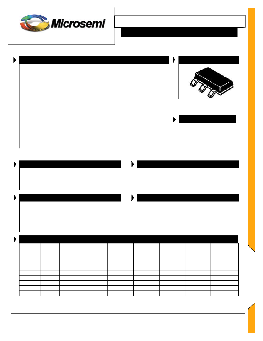
SOT 23-6L Packaging
M A X I M U M R A T I N G S
·
Operating Temperature: -55°C to +150°C
·
Storage Temperature: -55°C to +150°C
·
Peak Pulse power 200 watts (8/20 µs Figure 1)
·
SOT 23-6L Packaging
M E C H A N I C A L
·
Molded SOT23-6L Surface Mount
·
Weight .014 grams (approximate)
·
Body Marked with device number
·
Part is symmetrical therefore pin one can be
defined as either one of the four corner pins (for
clarification see schematic on page 2)
P A C K A G I N G
·
Tape & Reel per EIA Standard 481
·
3,000 pieces per 7 inch reel
SMS03 thru SMS24

Microsemi
Scottsdale Division
8700 E. Thomas Rd. PO Box 1390, Scottsdale, AZ 85252 USA, (480) 941-6300, Fax: (480) 947-1503
Page 2
Copyright
©
2000
MSC1686.PDF 2-14-2001 REV C
WWW.
Microsemi
.
COM
SMS03 thru SMS24
4 LINE UNIDIRECTIONAL TVSarray TM
PRODUCT PREVIEW
S C O T T S D A L E D I V I S I O N
S Y M B O L S & D E F I N I T I O N S
Symbol
DEFINITION
V
WM
Rated stand off voltage: Maximum dc voltage that can be applied over the operating temperature range. Vwm
must be selected to be equal or be greater than the operating voltage of the line to be protected
V
BR
Minimum Breakdown Voltage: The minimum voltage the device will exhibit at a specified current
V
C
Clamping Voltage: Maximum clamping voltage across the TVS device when subjected to a given peak pulse
current at a pulse time of 20
µ
s.
I
D
Standby Current: Leakage current at V
WM.
C
Capacitance: Capacitance of the TVS as defined @ 0 volts at a frequency of 1 MHz and stated in Pico Farads.
G R A P H S
P A C K A G I N G A N D S C H E M A T I C
8/20µs 200W Pulse
.1
1
10
100
1000
FIGURE 1
Peak Pulse Power Vs Pulse Time t=µsec
FIGURE 2
Pulse Wave Form
Ppp Peak Pulse Power (Kw)
10
1
.01
0.001
DIMENSIONS MILLIMETERS
DIMENSIONS INCHES
DIM
MIN
NOM
MAX
MIN
NOM
MAX
A
2.70
2.90
3.10
.106
.114
.127
A1
0.00
0.10
.000
.004
A2
1.00
1.10
1.30
.039
.043
.051
B
0.35
0.40
0.50
.014
.016
.020
C
0.10
0.15
0.25
.004
.006
.010
D
1.50
1.60
1.80
.059
.063
.071
E
1.70
1.90
2.10
.067
.075
.083
F
2.60
2.80
3.00
.102
.110
.118
G
0.20
.008
GRAPHS PACKAGE
DATA