
PRODUCTS AND SPECIFICATIONS DISCUSSED HEREIN ARE SUBJECT TO CHANGE BY MICRON WITHOUT NOTICE.
1
256Mb: x4, x8, x16 SDRAM
Micron Technology, Inc., reserves the right to change products or specifications without notice.
256MSDRAM_F.p65 Rev. F; Pub. 1/03
©2003, Micron Technology, Inc.
256Mb: x4, x8, x16
SDRAM
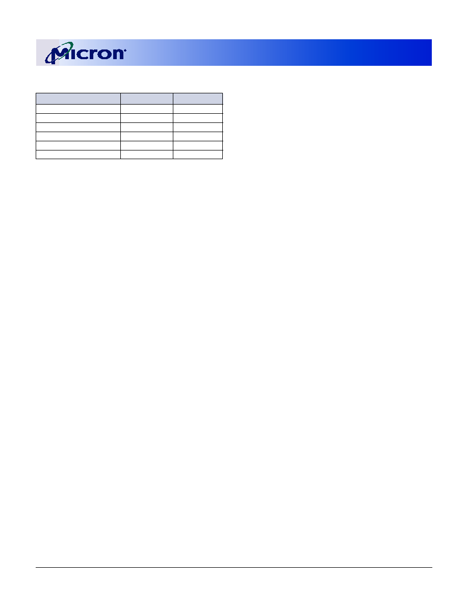
KEY TIMING PARAMETERS
SPEED
CLOCK
ACCESS TIME
SETUP
HOLD
GRADE
FREQUENCY CL = 2* CL = 3*
TIME
TIME
-7E
143 MHz
5.4ns
1.5ns
0.8ns
-75
133 MHz
5.4ns
1.5ns
0.8ns
-7E
133 MHz
5.4ns
1.5ns
0.8ns
-75
100 MHz
6ns
1.5ns
0.8ns
64 Meg x 4
32 Meg x 8
16 Meg x 16
Configuration
16 Meg x 4 x 4 banks 8 Meg x 8 x 4 banks 4 Meg x 16 x 4 banks
Refresh Count
8K
8K
8K
Row Addressing
8K (A0A12)
8K (A0A12)
8K (A0A12)
Bank Addressing
4 (BA0, BA1)
4 (BA0, BA1)
4 (BA0, BA1)
Column Addressing
2K (A0A9, A11)
1K (A0A9)
512 (A0A8)
SYNCHRONOUS
DRAM
MT48LC64M4A2 16 Meg x 4
x 4 banks
MT48LC32M8A2 8 Meg x 8
x 4 banks
MT48LC16M16A2 4 Meg x 16 x 4 banks
For the latest data sheet, please refer to the Micron Web site:
www.micron.com/dramds
PIN ASSIGNMENT (Top View)
54-Pin TSOP
FEATURES
· PC66-, PC100-, and PC133-compliant
· Fully synchronous; all signals registered on
positive edge of system clock
· Internal pipelined operation; column address can
be changed every clock cycle
· Internal banks for hiding row access/precharge
· Programmable burst lengths: 1, 2, 4, 8, or full page
· Auto Precharge, includes CONCURRENT AUTO
PRECHARGE, and Auto Refresh Modes
· Self Refresh Mode
· 64ms, 8,192-cycle refresh
· LVTTL-compatible inputs and outputs
· Single +3.3V ±0.3V power supply
OPTIONS
MARKING
· Configurations
64 Meg x 4
(16 Meg x 4
x 4 banks)
64M4
32 Meg x 8
( 8 Meg x 8
x 4 banks)
32M8
16 Meg x 16 ( 4 Meg x 16 x 4 banks)
16M16
· WRITE Recovery (
t
WR)
t
WR = "2 CLK"
1
A2
· Package/Pinout
54-pin TSOP II OCPL
2
(400 mil)
TG
60-ball FBGA (8mm x 16mm) (x4, x8)
FB
4, 5
54-ball FBGA (8mm x 14mm) (x16 only)
FG
3
· Timing (Cycle Time)
7.5ns @ CL = 2 (PC133)
-7E
7.5ns @ CL = 3 (PC133)
-75
· Self Refresh
Standard
None
Low power
L
3
· Operating Temperature
Commercial (0
o
C to +70
o
C)
None
Industrial (-40
o
C to +85
o
C)
IT
3
NOTE: 1. Refer to Micron Technical Note TN-48-05.
2. Off-center parting line.
3. Consult Micron for availability.
4. Not available in x16 configuration.
5. Actual FBGA part marking shown on page 60.
Part Number Example:
MT48LC16M16A2TG-75
Note:
The # symbol indicates signal is active LOW. A dash ()
indicates x8 and x4 pin function is same as x16 pin function.
V
DD
DQ0
V
DD
Q
DQ1
DQ2
VssQ
DQ3
DQ4
V
DD
Q
DQ5
DQ6
VssQ
DQ7
V
DD
DQML
WE#
CAS#
RAS#
CS#
BA0
BA1
A10
A0
A1
A2
A3
V
DD
1
2
3
4
5
6
7
8
9
10
11
12
13
14
15
16
17
18
19
20
21
22
23
24
25
26
27
54
53
52
51
50
49
48
47
46
45
44
43
42
41
40
39
38
37
36
35
34
33
32
31
30
29
28
Vss
DQ15
VssQ
DQ14
DQ13
V
DD
Q
DQ12
DQ11
VssQ
DQ10
DQ9
V
DD
Q
DQ8
Vss
NC
DQMH
CLK
CKE
A12
A11
A9
A8
A7
A6
A5
A4
Vss
x8
x16
x16
x8
x4
x4
-
DQ0
-
NC
DQ1
-
NC
DQ2
-
NC
DQ3
-
NC
-
NC
-
-
-
-
-
-
-
-
-
-
-
-
-
NC
-
NC
DQ0
-
NC
NC
-
NC
DQ1
-
NC
-
NC
-
-
-
-
-
-
-
-
-
-
-
-
-
DQ7
-
NC
DQ6
-
NC
DQ5
-
NC
DQ4
-
NC
-
-
DQM
-
-
-
-
-
-
-
-
-
-
-
-
NC
-
NC
DQ3
-
NC
NC
-
NC
DQ2
-
NC
-
-
DQM
-
-
-
-
-
-
-
-
-
-
-
*CL = CAS (READ) latency

2
256Mb: x4, x8, x16 SDRAM
Micron Technology, Inc., reserves the right to change products or specifications without notice.
256MSDRAM_F.p65 Rev. F; Pub. 1/03
©2003, Micron Technology, Inc.
256Mb: x4, x8, x16
SDRAM
60-BALL FBGA ASSIGNMENT
(Top View)
64 Meg x 4 SDRAM
8mm x 16mm "FB"
32 Meg x 8 SDRAM
8mm x 16mm "FB"
NOTE: FBGA pin Symbol, Type, and Descriptions are identical to the listing of the 54-pin TSOP table on page 9.
A
B
C
D
E
F
G
H
J
K
L
M
N
P
R
1
2
3
4
5
6
7
8
Depopulated Balls
NC
Vss
NC
VssQ
V
DD
Q
DQ3
NC
NC
NC
VssQ
V
DD
Q
DQ2
NC
NC
NC
Vss
NC
DQM
NC
CK
A12
CKE
A11
A9
A8
A7
A6
A5
A4
Vss
V
DD
NC
V
DD
Q
NC
DQ0
VssQ
NC
NC
V
DD
Q
NC
DQ1
VssQ
NC
NC
V
DD
NC
WE#
CAS#
RAS#
NC
NC
CS#
BA1
BA0
A0
A10
A2
A1
V
DD
A3
A
B
C
D
E
F
G
H
J
K
L
M
N
P
R
1
2
3
4
5
6
7
8
Depopulated Balls
DQ7
Vss
NC
VssQ
V
DD
Q
DQ6
DQ5
NC
NC
VssQ
V
DD
Q
DQ4
NC
NC
NC
Vss
NC
DQM
NC
CK
A12
CKE
A11
A9
A8
A7
A6
A5
A4
Vss
V
DD
DQ0
V
DD
Q
NC
DQ1
VssQ
NC
DQ2
V
DD
Q
NC
DQ3
VssQ
NC
NC
V
DD
NC
WE#
CAS#
RAS#
NC
NC
CS#
BA1
BA0
A0
A10
A2
A1
V
DD
A3

3
256Mb: x4, x8, x16 SDRAM
Micron Technology, Inc., reserves the right to change products or specifications without notice.
256MSDRAM_F.p65 Rev. F; Pub. 1/03
©2003, Micron Technology, Inc.
256Mb: x4, x8, x16
SDRAM
54-BALL VFBGA ASSIGNMENT
(Top View)
16 Meg x 16 SDRAM
8mm x 14mm "FG"
A
B
C
D
E
F
G
H
J
1
2
3
4
5
6
7
8
9
Depopulated Balls
Vss
DQ15
DQ14
DQ13
DQ12
DQ11
DQ10
DQ9
DQ8
NC
UDQM
CLK
A12
A11
A8
A7
Vss
A5
V
SS
Q
V
DD
Q
V
SS
Q
V
DD
Q
Vss
CKE
A9
A6
A4
V
DD
Q
VssQ
V
DD
Q
V
SS
Q
V
DD
CAS#
BA0
A0
A3
DQ0
V
DD
DQ2
DQ1
DQ4
DQ3
DQ6
DQ5
LDQM
DQ7
RAS#
WE#
BA1
CS#
A1
A10
A2
V
DD
4
256Mb: x4, x8, x16 SDRAM
Micron Technology, Inc., reserves the right to change products or specifications without notice.
256MSDRAM_F.p65 Rev. F; Pub. 1/03
©2003, Micron Technology, Inc.
256Mb: x4, x8, x16
SDRAM
GENERAL DESCRIPTION
The 256Mb SDRAM is a high-speed CMOS,
dynamic random-access memory containing
268,435,456 bits. It is internally configured as a quad-
bank DRAM with a synchronous interface (all signals
are registered on the positive edge of the clock signal,
CLK). Each of the x4's 67,108,864-bit banks is orga-
nized as 8,192 rows by 2,048 columns by
4 bits. Each of the x8's 67,108,864-bit banks is orga-
nized as 8,192 rows by 1,024 columns by 8 bits. Each of
the x16's 67,108,864-bit banks is organized as 8,192
rows by 512 columns by 16 bits.
Read and write accesses to the SDRAM are burst
oriented; accesses start at a selected location and con-
tinue for a programmed number of locations in a pro-
grammed sequence. Accesses begin with the registra-
tion of an ACTIVE command, which is then followed by
a READ or WRITE command. The address bits regis-
tered coincident with the ACTIVE command are used
PART NUMBER ARCHITECTURE PACKAGE
MT48LC64M4A2TG
64 Meg x 4
54-pin TSOP II
MT48LC64M4A2FB*
64 Meg x 4
60-ball FBGA
MT48LC32M8A2TG
32 Meg x 8 54-pin TSOP II
MT48LC32M8A2FB*
32 Meg x 8 60-ball FBGA
MT48LC16M16A2TG
16 Meg x 16 54-pin TSOP II
MT48LC16M16A2FG
16 Meg x 16 54-ball FBGA
*Actual FBGA part marking shown on page 60.
256 Mb SDRAM PART NUMBERS
to select the bank and row to be accessed (BA0, BA1
select the bank; A0A12 select the row). The address
bits registered coincident with the READ or WRITE com-
mand are used to select the starting column location
for the burst access.
The SDRAM provides for programmable READ or
WRITE burst lengths of 1, 2, 4, or 8 locations, or the full
page, with a burst terminate option. An auto precharge
function may be enabled to provide a self-timed row
precharge that is initiated at the end of the burst se-
quence.
The 256Mb SDRAM uses an internal pipelined ar-
chitecture to achieve high-speed operation. This ar-
chitecture is compatible with the 2n rule of prefetch
architectures, but it also allows the column address to
be changed on every clock cycle to achieve a high-
speed, fully random access. Precharging one bank
while accessing one of the other three banks will hide
the precharge cycles and provide seamless, high-
speed, random-access operation.
The 256Mb SDRAM is designed to operate in 3.3V
memory systems. An auto refresh mode is provided,
along with a power-saving, power-down mode. All in-
puts and outputs are LVTTL-compatible.
SDRAMs offer substantial advances in DRAM oper-
ating performance, including the ability to synchro-
nously burst data at a high data rate with automatic
column-address generation, the ability to interleave
between internal banks to hide precharge time and
the capability to randomly change column addresses
on each clock cycle during a burst access.

5
256Mb: x4, x8, x16 SDRAM
Micron Technology, Inc., reserves the right to change products or specifications without notice.
256MSDRAM_F.p65 Rev. F; Pub. 1/03
©2003, Micron Technology, Inc.
256Mb: x4, x8, x16
SDRAM
TABLE OF CONTENTS
Functional Block Diagram 64 Meg x 4 ....................
6
Functional Block Diagram 32 Meg x 8 ....................
7
Functional Block Diagram 16 Meg x 16 ..................
8
Pin Descriptions .......................................................... 10
Ball Descriptions .......................................................... 10
Functional Description ............................................... 12
Initialization ........................................................... 12
Register Definition ................................................ 12
Mode Register ................................................... 12
Burst Length ................................................ 12
Burst Type ................................................... 13
CAS Latency ................................................ 14
Operating Mode .......................................... 14
Write Burst Mode ........................................ 14
Commands ................................................................... 15
Truth Table 1 (Commands and DQM Operation)
.............. 15
Command Inhibit .................................................. 16
No Operation (NOP) .............................................. 16
Load mode register ................................................ 16
Active ....................................................................... 16
Read ....................................................................... 16
Write ....................................................................... 16
Precharge ................................................................ 16
Auto Precharge ....................................................... 16
Burst Terminate ..................................................... 17
Auto Refresh ........................................................... 17
Self Refresh ............................................................. 17
Operation ..................................................................... 18
Bank/Row Activation ............................................. 18
Reads ....................................................................... 19
Writes ....................................................................... 25
Precharge ................................................................ 27
Power-Down ........................................................... 27
Clock Suspend ........................................................ 28
Burst Read/Single Write ....................................... 28
Concurrent Auto Precharge ................................. 29
Truth Table 2 (CKE)
...................................................... 31
Truth Table 3 (Current State, Same Bank)
........................ 32
Truth Table 4 (Current State, Different Bank)
.................. 34
Absolute Maximum Ratings ....................................... 36
DC Electrical Characteristics
and Operating Conditions ....................................... 36
I
DD
Specifications and Conditions ............................. 36
Capacitance .................................................................. 37
Electrical Characteristics
and Recommended AC Operating Conditions ....... 37
AC Electrical Characteristics (Timing Table) ......... 38
Timing Waveforms
Initialize and Load mode register ........................ 40
Power-Down Mode ................................................ 41
Clock Suspend Mode ............................................ 42
Auto Refresh Mode ................................................ 43
Self Refresh Mode .................................................. 44
Reads
Read Without Auto Precharge ..................... 45
Read With Auto Precharge ........................... 46
Single Read Without Auto Precharge ......... 47
Single Read With Auto Precharge ............... 48
Alternating Bank Read Accesses .................... 49
Read Full-Page Burst .................................... 50
Read DQM Operation ................................... 51
Writes
Write Without Auto Precharge ..................... 52
Write With Auto Precharge ........................... 53
Single Write - Without Auto Precharge ......... 54
Single Write - With Auto Precharge ................ 55
Alternating Bank Write Accesses ................... 56
Write Full-Page Burst .................................... 57
Write DQM Operation ................................... 58