2004 Microchip Technology Inc.
DS21893A-page 1
MCP73861/2
Features
� Linear Charge Management Controllers
- Integrated Pass Transistor
- Integrated Current Sense
- Reverse-Blocking Protection
� High-Accuracy Preset Voltage Regulation: + 0.5%
� Four Selectable Voltage Regulation Options:
- 4.1V, 4.2V - MCP73861
- 8.2V, 8.4V - MCP73862
� Programmable Charge Current: 1.2A Maximum
� Programmable Safety Charge Timers
� Preconditioning of Deeply Depleted Cells
� Automatic End-of-Charge Control
� Optional Continuous Cell Temperature Monitoring
� Charge Status Output for Direct LED Drive
� Fault Output for Direct LED Drive
� Automatic Power-Down
� Thermal Regulation
� Temperature Range: -40�C to 85�C
� Packaging: 16-Pin, 4 x 4 QFN
Applications
� Lithium-Ion/Lithium-Polymer Battery Chargers
� Personal Data Assistants
� Cellular Telephones
� Hand Held Instruments
� Cradle Chargers
� Digital Cameras
� MP3 Players
Description
The MCP7386X family of devices are highly advanced
linear charge management controllers for use in space-
limited, cost-sensitive applications. The MCP73861 and
MCP73862 combine high-accuracy constant voltage,
constant current regulation, cell preconditioning, cell
temperature monitoring, advanced safety timers, auto-
matic charge termination, internal current sensing,
reverse-blocking protection, and charge status and fault
indication in a space-saving 16-pin, 4 x 4 QFN package.
The MCP7386X provides a complete, fully-functional,
stand-alone charge management solution with a
minimum number of external components.
The MCP73861 is targeted for applicatioins utilizing
single-cell Lithium-Ion or Lithium-Polymer battery
packs, while the MCP73862 is targeted for dual series
cell Lithium-Ion or Lithium-Polymer battery packs. The
MCP73861 has two selectable voltage-regulation
options available (4.1V and 4.2V), for use with either
coke or graphite anodes, and operates with an input
voltage range of 4.5V to 12V. The MCP73862 has two
selectable voltage-regulation options available (8.2V
and 8.4V), for use with coke or graphite anodes, and
operates with an input voltage range of 8.7V to 12V.
The MCP7386X family of devices are fully specified
over the ambient temperature range of -40�C to +85�C.
Package Type
V
DD1
V
BAT1
THERM
EN
TIMER
STAT1 STAT2
1
2
3
4
14
15
16
PROG
V
DD2
V
SET
THREF
V
BAT3
V
BAT2
5
6
7
8
9
10
11
12
V
SS2
13
V
SS1
MCP73861
MCP73862
V
SS3
Advanced Single or Dual Cell, Fully Integrated Li-Ion /
Li-Polymer Charge Management Controllers

MCP73861/2
DS21893A-page 2
2004 Microchip Technology Inc.
Typical Application
Functional Block Diagram
EN
STAT1
STAT2
V
SET
V
DD
V
SS
TIMER
PROG
THERM
THREF
V
BAT3
V
BAT
+
-
Single
Lithium-Ion
Cell
2, 3
1
MCP73861
5
6
7
8
4, 9, 13
10, 11
12
14
16
15
5V
6.19 k
4.7�F
1.2A Lithium-Ion Battery Charger
4.7 �F
7.32 k
0.1
�F
+
-
Charge
Termination
Comparator
Voltage Control
Amplifier
+
-
U
VLO
COMPARATOR
V
UVLO
+
-
Temperature
Comparators
+
-
Bias and
Reference
Generator
V
UVLO
V
REF
(1.2V)
Power-On
Delay
+
�
+
-
V
REF
V
REF
Oscillator
I
REG
/12
Constant Voltage/
Recharge Comp.
Precondition
Control
Charge_OK
Precon
V
DD
Charge Current
Control Amplifier
+
�
V
REF
V
REF
+
-
Precondition
Comp.
Charge Control,
Charge Timers,
And
Status Logic
Drv Stat 2
Drv Stat 1
Charge_OK
I
REG
/12
V
DD1
THERM
EN
TIMER
STAT1
STAT2
V
BAT3
V
SS1
PROG
V
SET
THREF
V
BAT1
90
110k
10k
10k
100k
50k
50k
G=0.001
11k
1k
600k
(
1.65M
)
148.42k
1.58k
V
DD2
V
BAT2
300.04k
10.3k
(
8.58k
)
4k
Direction
Control
k
V
SS2
V
SS3
Values in ( )
reflect the
MCP73862
device

2004 Microchip Technology Inc.
DS21893A-page 3
MCP73861/2
1.0
ELECTRICAL
CHARACTERISTICS
Absolute Maximum Ratings
V
DD
N
...............................................................................13.5V
V
BATN
, V
SET
, EN, STAT1, STAT2 w.r.t. V
SS
.................................................................. -0.3 to (V
DD
+0.3)V
PROG, THREF, THERM, TIMER w.r.t. V
SS
..............-0.3 to 6V
Maximum Junction Temperature, T
J
............ Internally Limited
Storage temperature .....................................-65�C to +150�C
ESD protection on all pins:
Human Body Model (1.5 k
in series with 100 pF)
....
4 kV
Machine Model (200 pF, No series resistance) ...........300V
Notice: Stresses above those listed under "Maximum Rat-
ings" may cause permanent damage to the device. This is a
stress rating only and functional operation of the device at
those or any other conditions above those indicated in the
operational listings of this specification is not implied. Expo-
sure to maximum rating conditions for extended periods may
affect device reliability.
DC CHARACTERISTICS
Electrical Specifications: Unless otherwise indicated, all limits apply for V
DD
= [V
REG
(Typ) + 0.3V] to 12V,
T
A
= -40�C to 85�C. Typical values are at +25�C, V
DD
= [V
REG
(typ.) + 1.0V]
Parameters
Sym
Min
Typ
Max
Units
Conditions
Supply Input
Supply Voltage
V
DD
4.5
--
12
V
MCP73861
8.7
--
12
V
MCP73862
Supply Current
I
SS
--
0.17
4
�A
Disabled
--
0.53
4
mA
Operating
UVLO Start Threshold
V
START
4.25
4.5
4.65
V
MCP73861
8.45
8.8
9.05
V
MCP73862
V
DD
Low-to-High
UVLO Stop Threshold
V
STOP
4.20
4.4
4.55
V
MCP73861
8.40
8.7
8.95
V
MCP73862
V
DD
High-to-Low
Voltage Regulation (Constant Voltage Mode)
Regulated Output Voltage
V
REG
4.079
4.1
4.121
V
MCP73861, V
SET
= V
SS
4.179
4.2
4.221
V
MCP73861, V
SET
= V
DD
8.159
8.2
8.241
V
MCP73862, V
SET
= V
SS
8.358
8.4
8.442
V
MCP73862, V
SET
= V
DD
V
DD
= [V
REG
(Typ) + 1V], I
OUT
=10 mA
T
A
= -5�C to +55�C
Line Regulation
|(
V
BAT
/
V
BAT
)| /
V
DD
--
0.025
0.25
%/V
V
DD
= [V
REG
(Typ)+1V] to 12V
I
OUT
= 10 mA
Load Regulation
|
V
BAT
/V
BAT
|
--
0.01
0.25
%
I
OUT
= 10 mA to 150 mA
V
DD
= [V
REG
(Typ)+1V]
Supply Ripple Attenuation
PSRR
--
60
--
dB
I
OUT
= 10 mA, 10Hz to 1 kHz
--
42
--
dB
I
OUT
= 10 mA, 10Hz to 10 kHz
--
28
--
dB
I
OUT
= 10 mA, 10Hz to 1 MHz
Output Reverse-Leakage
Current
I
DISCHARGE
--
0.23
1
�A
V
DD
< V
BAT
= V
REG
(Typ)
Current Regulation (Fast Charge Constant Current Mode)
Fast Charge Current
Regulation
I
REG
85
100
115
mA
PROG = OPEN
1020
1200
1380
mA
PROG = V
SS
425
500
575
mA
PROG = 1.6 k
T
A
= -5�C to +55�C
MCP73861/2
DS21893A-page 4
2004 Microchip Technology Inc.
Preconditioning Current Regulation (Trickle Charge Constant Current Mode)
Precondition Current
Regulation
I
PREG
5
10
15
mA
PROG = OPEN
60
120
180
mA
PROG = V
SS
25
50
75
mA
PROG = 1.6 k
T
A
=-5�C to +55�C
Precondition Threshold
Voltage
V
PTH
2.70
2.80
2.90
V
MCP73861, V
SET
= V
SS
2.75
2.85
2.95
V
MCP73861, V
SET
= V
DD
5.40
5.60
5.80
V
MCP73862, V
SET
= V
SS
5.50
5.70
5.90
V
MCP73862, V
SET
= V
DD
V
BAT
Low-to-High
Charge Termination
Charge Termination Current
I
TERM
6
8.5
11
mA
PROG = OPEN
70
90
120
mA
PROG = V
SS
32
41
50
mA
PROG = 1.6 k
T
A
=-5�C to +55�C
Automatic Recharge
Recharge Threshold
Voltage
V
RTH
V
REG
-
300mV
V
REG
-
200mV
V
REG
-
100mV
V
MCP73861
V
REG
-
600mV
V
REG
-
400mV
V
REG
-
200mV
V
MCP73862
V
BAT
High-to-Low
Thermistor Reference
Thermistor Reference
Output Voltage
V
THREF
2.475
2.55
2.625
V
T
A
= 25�C, V
DD
= V
REG
(typ.) + 1V,
I
THREF
= 0 mA
Thermistor Reference
Source Current
I
THREF
200
--
--
�A
Thermistor Reference Line
Regulation
|(
V
THREF
/
V
THREF
)|/
V
DD
-
0.1
0.25
%/V
V
DD
= [V
REG
(Typ) + 1V] to 12V
Thermistor Reference Load
Regulation
|
V
THREF
/
V
THREF|
0.01
0.10
%
I
THREF
= 0 mA to 0.20 mA
Thermistor Comparator
Upper Trip Threshold
V
T1
1.18
1.25
1.32
V
Upper Trip Point Hysteresis
V
T1HYS
--
-50
--
mV
Lower Trip Threshold
V
T2
0.59
0.62
0.66
V
Lower Trip Point Hysteresis
V
T2HYS
--
80
--
mV
Input Bias Current
I
BIAS
--
--
2
�
A
Status Indicator - STAT1, STAT2
Sink Current
I
SINK
4
8
12
mA
Low Output Voltage
V
OL
--
200
400
mV
I
SINK
= 1 mA
Input Leakage Current
I
LK
--
0.01
1
�
A
I
SINK
= 0 mA, V
STAT1,2
= 12V
Enable Input
Input High Voltage Level
V
IH
1.4
--
--
V
Input Low Voltage Level
V
IL
--
--
0.8
V
Input Leakage Current
I
LK
--
0.01
1
�
A
V
ENABLE
= 12V
DC CHARACTERISTICS (Continued)
Electrical Specifications: Unless otherwise indicated, all limits apply for V
DD
= [V
REG
(Typ) + 0.3V] to 12V,
T
A
= -40�C to 85�C. Typical values are at +25�C, V
DD
= [V
REG
(typ.) + 1.0V]
Parameters
Sym
Min
Typ
Max
Units
Conditions

2004 Microchip Technology Inc.
DS21893A-page 5
MCP73861/2
TEMPERATURE SPECIFICATIONS
Thermal Shutdown
Die Temperature
T
SD
--
155
--
�C
Die Temperature Hysteresis
T
SDHYS
--
10
--
�C
DC CHARACTERISTICS (Continued)
Electrical Specifications: Unless otherwise indicated, all limits apply for V
DD
= [V
REG
(Typ) + 0.3V] to 12V,
T
A
= -40�C to 85�C. Typical values are at +25�C, V
DD
= [V
REG
(typ.) + 1.0V]
Parameters
Sym
Min
Typ
Max
Units
Conditions
AC CHARACTERISTICS
Electrical Specifications: Unless otherwise indicated, all limits apply for V
DD
= [V
REG
(typ.) + 0.3V] to 12V,
T
A
= -40�C to 85�C. Typical values are at +25�C, V
DD
= [V
REG
(typ.) + 1.0V]
Parameters
Sym
Min
Typ
Max
Units
Conditions
UVLO Start Delay
t
START
--
--
5
ms
V
DD
Low to High
Current Regulation
Transition Time Out of
Preconditioning
t
DELAY
--
--
1
ms
V
BAT
< V
PTH
to V
BAT
> V
PTH
Current Rise Time Out of
Preconditioning
t
RISE
--
--
1
ms
I
OUT
Rising to 90% of I
REG
Fast Charge Safety Timer
Period
t
FAST
1.1
1.5
1.9
Hours
C
TIMER
= 0.1 �F
Preconditioning Current Regulation
Preconditioning Charge
Safety Timer Period
t
PRECON
45
60
75
Minutes C
TIMER
= 0.1 �F
Charge Termination
Elapsed Time Termination
Period
t
TERM
2.2
3
3.8
Hours
C
TIMER
= 0.1 �F
Status Indicators
Status Output turn-off
t
OFF
--
--
200
�s
I
SINK
= 1 mA to 0 mA
Status Output turn-on
t
ON
--
--
200
�s
I
SINK
= 0 mA to 1 mA
Electrical Specifications: Unless otherwise indicated, all limits apply for V
DD
= [V
REG
(typ.) + 0.3V] to 12V.
Typical values are at +25�C, V
DD
= [V
REG
(typ.) + 1.0V]
Parameters
Sym
Min
Typ
Max
Units
Conditions
Temperature Ranges
Specified Temperature Range
T
A
-40
--
+85
�C
Operating Temperature Range
T
J
-40
--
+125
�C
Storage Temperature Range
T
A
-65
--
+150
�C
Thermal Package Resistances
Thermal Resistance, 16-L, 4mm x 4mm QFN
JA
--
37
--
�C/W
4-Layer JC51-7 Standard
Board, Natural Convection

MCP73861/2
DS21893A-page 6
2004 Microchip Technology Inc.
2.0
TYPICAL PERFORMANCE CURVES
NOTE: Unless otherwise indicated, V
DD
= [V
REG
(Typ) + 1V], I
OUT
= 10 mA and T
A
= +25�C, Constant Voltage mode.
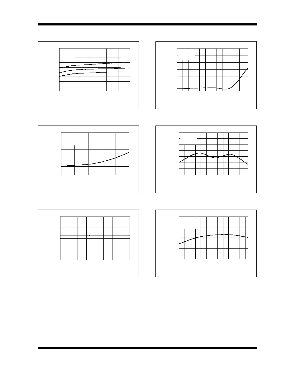
FIGURE 2-1:
Battery Regulation Voltage
(V
BAT
) vs. Charge Current (I
OUT
).
FIGURE 2-2:
Battery Regulation Voltage
(V
BAT
) vs. Supply Voltage (V
DD
).
FIGURE 2-3:
Battery Regulation Voltage
(V
BAT
) vs. Supply Voltage (V
DD
).
FIGURE 2-4:
Supply Current (I
SS
) vs.
Charge Current (I
OUT
).
FIGURE 2-5:
Supply Current (I
SS
) vs.
Supply Voltage (V
DD
).
FIGURE 2-6:
Supply Current (I
SS
) vs.
Supply Voltage (V
DD
).
Note:
The graphs and tables provided following this note are a statistical summary based on a limited number of
samples and are provided for informational purposes only. The performance characteristics listed herein
are not tested or guaranteed. In some graphs or tables, the data presented may be outside the specified
operating range (e.g., outside specified power supply range) and therefore outside the warranted range.
4.193
4.195
4.197
4.199
4.201
4.203
4.205
4.207
10
100
1000
I
OUT
(mA)
V
BAT
(V)
MCP73861
V
SET
= V
DD
V
DD
= 5.2V
3.80
3.90
4.00
4.10
4.20
4.30
4.40
4.5
6.0
7.5
9.0
10.5
12.0
V
DD
(V)
V
BAT
(V)
MCP73861
V
SET
= V
DD
I
OUT
= 1000 mA
4.193
4.195
4.197
4.199
4.201
4.203
4.205
4.207
4.5
6.0
7.5
9.0
10.5
12.0
V
DD
(V)
V
BAT
(V)
MCP73861
V
SET
= V
DD
I
OUT
= 10 mA
0.40
0.50
0.60
0.70
0.80
0.90
1.00
10
100
1000
I
OUT
(mA)
I
SS
(mA
)
MCP73861
V
SET
= V
DD
V
DD
= 5.2V
0.40
0.60
0.80
1.00
1.20
1.40
1.60
4.5
6.0
7.5
9.0
10.5
12.0
V
DD
(V)
I
SS
(mA
)
MCP73861
V
SET
= V
DD
I
OUT
= 1000 mA
0.40
0.50
0.60
0.70
0.80
0.90
1.00
4.5
6.0
7.5
9.0
10.5
12.0
V
DD
(V)
I
SS
(mA
)
MCP73861
V
SET
= V
DD
I
OUT
= 10 mA
2004 Microchip Technology Inc.
DS21893A-page 7
MCP73861/2
NOTE: Unless otherwise indicated, V
DD
= [V
REG
(Typ) + 1V], I
OUT
= 10 mA and T
A
= +25�C, Constant Voltage mode.
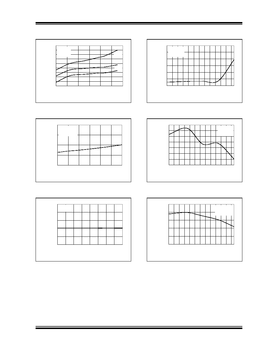
FIGURE 2-7:
Output Leakage Current
(I
DISCHARGE
) vs. Battery Voltage (V
BAT
).
FIGURE 2-8:
Thermistor Reference
Voltage (V
THREF
) vs. Supply Voltage (V
DD
).
FIGURE 2-9:
Thermistor Reference
Voltage (V
THREF
) vs. Thermistor Bias Current
(I
THREF
).
FIGURE 2-10:
Supply Current (I
SS
) vs.
Ambient Temperature (T
A
).
FIGURE 2-11:
Battery Regulation Voltage
(V
BAT
) vs. Ambient Temperature (T
A
).
FIGURE 2-12:
Thermistor Reference
Voltage (V
THREF
) vs. Ambient Temperature (T
A
).
0.00
0.05
0.10
0.15
0.20
0.25
0.30
0.35
0.40
0.45
2.0
2.4
2.8
3.2
3.6
4.0
4.4
V
BAT
(V)
I
DISCHARGE
(
�
A)
MCP73861
V
SET
= V
DD
V
DD
= V
SS
+25�C
-40�C
+85�C
2.500
2.510
2.520
2.530
2.540
2.550
4.5
6.0
7.5
9.0
10.5
12.0
V
DD
(V)
V
T
HREF
(V
)
MCP73861
V
SET
= V
DD
I
THREF
= 100 �A
2.500
2.505
2.510
2.515
2.520
0
25
50
75
100
125
150
175
200
I
THREF
(�A)
V
T
HREF
(V
)
MCP73861
V
SET
= V
DD
0.40
0.60
0.80
1.00
1.20
1.40
1.60
-40 -30 -20 -10 0 10 20 30 40 50 60 70 80
T
A
(�C)
I
SS
(mA
)
MCP73861
V
SET
= V
DD
I
OUT
= 10 mA
4.193
4.195
4.197
4.199
4.201
4.203
4.205
4.207
-40
-30
-20
-10
0
10
20
30
40
50
60
70
80
T
A
(�C)
V
BAT
(V
)
MCP73861
V
SET
= V
DD
I
OUT
= 10 mA
2.500
2.505
2.510
2.515
2.520
-40
-30
-20
-10
0
10
20
30
40
50
60
70
80
T
A
(�C)
V
T
HREF
(V)
MCP73861
V
SET
= V
DD
I
THREF
= 100
�
A

MCP73861/2
DS21893A-page 8
2004 Microchip Technology Inc.
NOTE: Unless otherwise indicated, V
DD
= [V
REG
(Typ) + 1V], I
OUT
= 10 mA and T
A
= +25�C, Constant Voltage mode.
FIGURE 2-13:
Battery Regulation Voltage
(V
BAT
) vs. Charge Current (I
OUT
).
FIGURE 2-14:
Battery Regulation Voltage
(V
BAT
) vs. Supply Voltage (V
DD
).
FIGURE 2-15:
Battery Regulation Voltage
(V
BAT
) vs. Supply Voltage (V
DD
).
FIGURE 2-16:
Supply Current (I
SS
) vs.
Charge Current (I
OUT
).
FIGURE 2-17:
Supply Current (I
SS
) vs.
Supply Voltage (V
DD
).
FIGURE 2-18:
Supply Current (I
SS
) vs.
Supply Voltage (V
DD
).
8.393
8.395
8.397
8.399
8.401
8.403
8.405
8.407
10
100
1000
I
OUT
(mA)
V
BAT
(V
)
MCP73862
V
SET
= V
DD
V
DD
= 9.4V
8.393
8.395
8.397
8.399
8.401
8.403
8.405
8.407
10.0
10.4
10.8
11.2
11.6
12.0
V
DD
(V)
V
BAT
(V
)
MCP73862
V
SET
= V
DD
I
OUT
= 1000 mA
8.398
8.400
8.402
8.404
8.406
8.408
8.410
8.412
9.0
9.5
10.0
10.5
11.0
11.5
12.0
V
DD
(V)
V
BAT
(V
)
MCP73862
V
SET
= V
DD
I
OUT
= 10 mA
0.40
0.50
0.60
0.70
0.80
0.90
1.00
10
100
1000
I
OUT
(mA)
I
SS
(m
A
)
MCP73862
V
SET
= V
DD
V
DD
= 9.4V
0.40
0.60
0.80
1.00
1.20
1.40
1.60
9.0
9.5
10.0
10.5
11.0
11.5
12.0
V
DD
(V)
I
SS
(m
A
)
MCP73862
V
SET
= V
DD
I
OUT
= 1000 mA
0.40
0.50
0.60
0.70
0.80
0.90
1.00
9.0
9.5
10.0
10.5
11.0
11.5
12.0
V
DD
(V)
I
SS
(m
A
)
MCP73862
V
SET
= V
DD
I
OUT
= 10 mA
2004 Microchip Technology Inc.
DS21893A-page 9
MCP73861/2
NOTE: Unless otherwise indicated, V
DD
= [V
REG
(Typ) + 1V], I
OUT
= 10 mA and T
A
= +25�C, Constant Voltage mode.
FIGURE 2-19:
Output Leakage Current
(I
DISCHARGE
) vs. Battery Voltage (V
BAT
).
FIGURE 2-20:
Thermistor Reference
Voltage (V
THREF
) vs. Supply Voltage (V
DD
).
FIGURE 2-21:
Thermistor Reference
Voltage (V
THREF
) vs. Thermistor Bias Current
(I
THREF
).
FIGURE 2-22:
Supply Current (I
SS
) vs.
Ambient Temperature (T
A
).
FIGURE 2-23:
Battery Regulation Voltage
(V
BAT
) vs. Ambient Temperature (T
A
).
FIGURE 2-24:
Thermistor Reference
Voltage (V
THREF
) vs. Ambient Temperature (T
A
).
0.00
0.05
0.10
0.15
0.20
0.25
0.30
0.35
0.40
0.45
4.0
4.8
5.6
6.4
7.2
8.0
8.8
V
BAT
(V)
I
DISCHARGE
(m
A
)
MCP73862
V
SET
= V
DD
V
DD
= V
SS
+25�C
-40�C
+85�C
2.530
2.540
2.550
2.560
2.570
9.0
9.5
10.0
10.5
11.0
11.5
12.0
V
DD
(V)
V
T
HREF
(V
)
MCP73862
V
SET
= V
DD
I
THREF
= 100
�
A
2.540
2.542
2.544
2.546
2.548
2.550
0
25
50
75
100
125
150
175
200
I
THREF
(�A)
V
T
HREF
(V
)
MCP73862
V
SET
= V
DD
0.40
0.60
0.80
1.00
1.20
1.40
1.60
-40
-30
-20
-10
0
10
20
30
40
50
60
70
80
T
A
(�C)
I
SS
(m
A
)
MCP73862
V
SET
= V
DD
I
OUT
= 10 mA
8.386
8.390
8.394
8.398
8.402
8.406
8.410
8.414
-40
-30
-20
-10
0
10
20
30
40
50
60
70
80
T
A
(�C)
V
BAT
(V
)
MCP73862
V
SET
= V
DD
I
OUT
= 10 mA
2.530
2.534
2.538
2.542
2.546
2.550
-40
-30
-20
-10
0
10
20
30
40
50
60
70
80
T
A
(�C)
V
T
HREF
(V
)
MCP73862
V
SET
= V
DD
I
THREF
= 100
�
A
MCP73861/2
DS21893A-page 10
2004 Microchip Technology Inc.
NOTE: Unless otherwise indicated, V
DD
= [V
REG
(Typ) + 1V], I
OUT
= 10 mA and T
A
= +25�C, Constant Voltage mode.
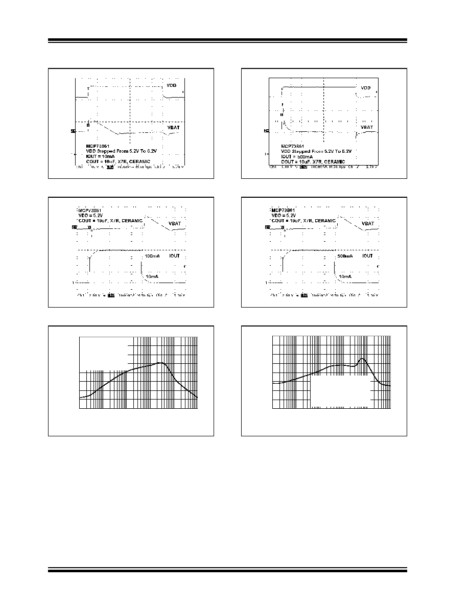
FIGURE 2-25:
Line Transient Response.
FIGURE 2-26:
Load Transient Response.
FIGURE 2-27:
Power Supply Ripple
Rejection.
FIGURE 2-28:
Line Transient Response.
FIGURE 2-29:
Load Transient Response.
FIGURE 2-30:
Power Supply Ripple
Rejection.
-80
-70
-60
-50
-40
-30
-20
-10
0
0.01
0.1
1
10
100
1000
Frequency (kHz)
A
ttenuation (dB
)
MCP73861
V
DD
= 5.2V
V
AC
= 100 mVp-p
I
OUT
= 10 mA
C
OUT
= 10
�
F, Ceramic
-80
-70
-60
-50
-40
-30
-20
-10
0
0.01
0.1
1
10
100
1000
Frequency (kHz)
A
ttenuation (dB
)
MCP73861
V
DD
= 5.2V
V
AC
= 100 mVp-p
I
OUT
= 100 mA
C
OUT
= 10
�
F, X7R, Ceramic

2004 Microchip Technology Inc.
DS21893A-page 11
MCP73861/2
NOTE: Unless otherwise indicated, V
DD
= [V
REG
(Typ) + 1V], I
OUT
= 10 mA and T
A
= +25�C, Constant Voltage mode.
FIGURE 2-31:
Charge Current (I
OUT
) vs.
Programming Resistor (R
PROG
).
FIGURE 2-32:
Charge Current (I
OUT
) vs.
Ambient Temperature (T
A
).
0
200
400
600
800
1000
1200
OPEN
4.8K
1.6K
536
0
R
PROG
(
)
I
OUT
(m
A
)
MCP73861/2
V
SET
= V
DD
493
495
497
499
501
503
505
-40
-30
-20
-10
0
10
20
30
40
50
60
70
80
T
A
(�C)
I
OUT
(m
A
)
MCP73861/2
V
SET
= V
DD
R
PROG
= 1.6 k

MCP73861/2
DS21893A-page 12
2004 Microchip Technology Inc.
3.0
PIN DESCRIPTION
The descriptions of the pins are listed in Table 3-1.
TABLE 3-1:
PIN FUNCTION TABLES
3.1
Voltage Regulation Selection
(V
SET
)
MCP73861: Connect to V
SS
for 4.1V regulation
voltage, connect to V
DD
for 4.2V regulation voltage.
MCP73862: Connect to V
SS
for 8.2V regulation
voltage, connect to V
DD
for 8.4V regulation voltage.
3.2
Battery Management Input Supply
(V
DD2
, V
DD1
)
A supply voltage of [V
REG
(Typ) + 0.3V] to 12V is
recommended. Bypass to V
SS
with a minimum of
4.7 �F.
3.3
Battery Management 0V Reference
(V
SS1
, V
SS2
, V
SS3
)
Connect to negative terminal of battery and input
supply.
3.4
Current Regulation Set (PROG)
Preconditioning, fast and termination currents are
scaled by placing a resistor from PROG to V
SS
.
3.5
Cell Temperature Sensor Bias
(THREF)
Voltage reference to bias external thermistor for contin-
uous cell-temperature monitoring and pre-qualification.
3.6
Cell Temperature Sensor Input
(THERM)
Input for an external thermistor for continuous cell-
temperature monitoring and pre-qualification. Connect
to THREF/3 to disable temperature sensing.
3.7
Timer Set
All safety timers are scaled by C
TIMER
/0.1 �F.
3.8
Battery Charge Control Output
(V
BAT1
, V
BAT2
)
Connect to positive terminal of battery. Drain terminal
of internal P-channel MOSFET pass transistor. Bypass
to V
SS
with a minimum of 4.7
�
F to ensure loop stability
when the battery is disconnected.
3.9
Battery Voltage Sense (V
BAT3
)
Voltage sense input. Connect to positive terminal of
battery. A precision internal resistor divider regulates
the final voltage on this pin to V
REG
.
3.10
Logic Enable (EN)
Input to force charge termination, initiate charge, clear
faults or disable automatic recharge.
3.11
Fault Status Output (STAT2)
Current-limited, open-drain drive for direct connection
to a LED for charge status indication. Alternatively, a
pull-up resistor can be applied for interfacing to a host
microcontroller.
3.12
Charge Status Output (STAT1)
Current limited, open-drain drive for direct connection
to an LED for charge status indication. Alternatively, a
pull-up resistor can be applied for interfacing to a host
microcontroller.
Pin No.
Symbol
Function
1
V
SET
Voltage Regulation Selection
2
V
DD1
Battery Management Input Supply
3
V
DD2
Battery Management Input Supply
4
V
SS1
Battery Management 0V Reference
5
PROG
Current Regulation Set
6
THREF
Cell Temperature Sensor Bias
7
THERM
Cell Temperature Sensor Input
8
TIMER
Timer Set
9
V
SS3
Battery Management 0V Reference
10
V
BAT1
Battery Charge Control Output
11
V
BAT2
Battery Charge Control Output
12
V
BAT3
Battery Voltage Sense
13
V
SS2
Battery Management 0V Reference
14
EN
Logic Enable
15
STAT2
Fault Status Output
16
STAT1
Charge Status Output

2004 Microchip Technology Inc.
DS21893A-page 13
MCP73861/2
4.0
DEVICE OVERVIEW
The MCP7386X family of devices are highly advanced
linear charge management controllers. Refer to the
functional block diagram. Figure 4-2 depicts the opera-
tional flow algorithm from charge initiation to
completion and automatic recharge.
4.1
Charge Qualification and
Preconditioning
Upon insertion of a battery or application of an external
supply, the MCP7386X family of devices automatically
performs a series of safety checks to qualify the
charge. The input source voltage must be above the
undervoltage lockout threshold, the enable pin must be
above the logic-high level and the cell temperature
must be within the upper and lower thresholds. The
qualification parameters are continuously monitored.
Deviation beyond the limits automatically suspends or
terminates the charge cycle. The input voltage must
deviate below the undervoltage lockout stop threshold
for at least one clock period to be considered valid.
After the qualification parameters have been met, the
MCP7386X initiates a charge cycle. The charge status
output is pulled low throughout the charge cycle (see
Table 5-1 for charge status outputs). If the battery volt-
age is below the preconditioning threshold (V
PTH
) the
MCP7386X preconditions the battery with a trickle-
charge. The preconditioning current is set to approxi-
mately 10% of the fast charge regulation current. The
preconditioning trickle-charge safely replenishes
deeply depleted cells and minimizes heat dissipation
during the initial charge cycle. If the battery voltage has
not exceeded the preconditioning threshold before the
preconditioning timer has expired, a fault is indicated
and the charge cycle is terminated.
4.2
Constant Current Regulation -
Fast Charge
Preconditioning ends, and fast charging begins, when
the battery voltage exceeds the preconditioning thresh-
old. Fast charge regulates to a constant current (I
REG
),
which is set via an external resistor connected to the
PROG pin. Fast charge continues until the battery volt-
age reaches the regulation voltage (V
REG
), or the fast
charge timer expires; in which case, a fault is indicated
and the charge cycle is terminated.
4.3
Constant Voltage Regulation
When the battery voltage reaches the regulation volt-
age (V
REG
) constant voltage regulation begins. The
MCP7386X monitors the battery voltage at the V
BAT
pin. This input is tied directly to the positive terminal of
the battery. The MCP7386X selects the voltage regula-
tion value based on the state of the V
SET
. With V
SET
tied to V
SS
, the MCP73861 and MCP73862 regulate to
4.1V and 8.2V, respectively. With V
SET
tied to V
DD
, the
MCP73861 and MCP73862 regulate to 4.2V and 8.4V,
respectively.
4.4
Charge Cycle Completion and
Automatic Re-Charge
The MCP7386X monitors the charging current during
the constant voltage regulation phase. The charge cycle
is considered complete when the charge current has
diminished below approximately 8% of the regulation
current (I
REG
) or the elapsed timer has expired.
The MCP7386X automatically begins a new charge
cycle when the battery voltage falls below the recharge
threshold (V
RTH
) assuming all the qualification
parameters are met.
4.5
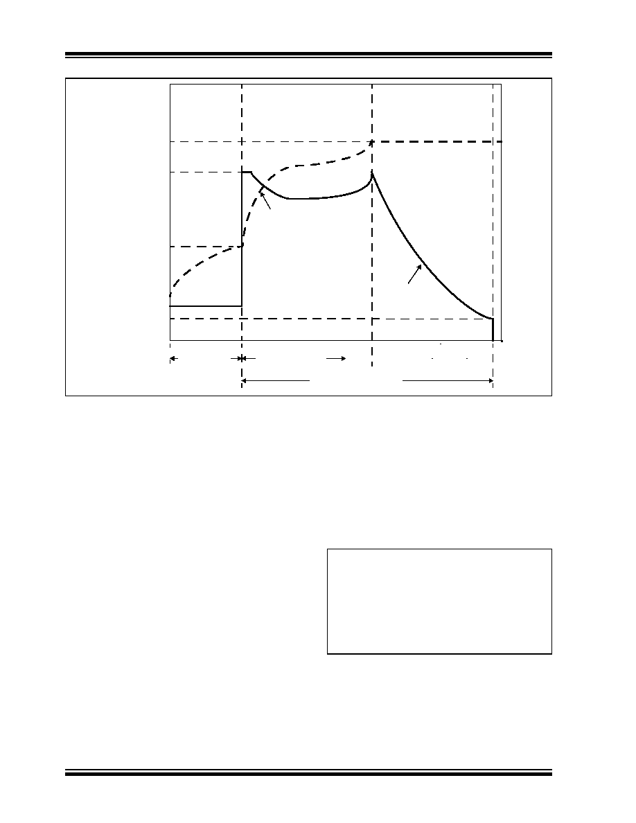
Thermal Regulation
The MCP7386X family limits the charge current based
on the die temperature. Thermal regulation optimizes
the charge cycle time while maintaining device reliabil-
ity. If thermal regulation is entered, the timer is automat-
ically slowed down to ensure that a charge cycle will
not terminate prematurely. Figure 4-1 depicts the
thermal regulation profile.
FIGURE 4-1:
Typical Maximum Charge
Current vs. Die Temperature.
4.6
Thermal Shutdown
The MCP7386X family suspends charge if the die tem-
perature exceeds 155�C. Charging will resume when
the die temperature has cooled by approximately 10�C.
The thermal shutdown is a secondary safety feature in
the event that there is a failure within the thermal
regulation circuitry.
0
200
400
600
800
1000
1200
1400
0
20
40
60
80
100
120
140
Die Temperature (� C)
M
axi
mu
m Ch
arg
e
Cu
rren
t
(mA)
Minimum
Maximum

MCP73861
/2
DS2
1893A-page
14
20
04 M
i
c
r
ochip
T
e
c
hnology
I
n
c
.
FIGURE 4-2:
Operational Flow Algorithm.
Preconditioning Phase
Charge Current = I
PREG
Reset Safety Timer
Yes
Initialize
No
Yes
V
BAT
> V
PTH
STAT1 = On
V
BAT
> V
PTH
Yes
V
DD
< V
UVLO
No
No
Safety Timer
Yes
Temperature OK
No
STAT1 = Off
Safety Timer Suspended
Charge Current = 0
Fault
Charge Current = 0
Reset Safety Timer
or EN Low
No
STAT1 = Off
Constant Current
Charge Current = I
REG
Reset Safety Timer
V
BAT
= V
REG
No
No
Safety Timer
Yes
Temperature OK
Constant Voltage Phase
Output Voltage = V
REG
I
OUT
< I
TERM
Yes
V
BAT
< V
RTH
Elapsed Timer
Charge Termination
Charge Current = 0
Reset Safety Timer
No
STAT1 = Flashing
Yes
Yes
Temperature OK
No
STAT1 = Flashing
Safety Timer Suspended
Charge Current = 0
Yes
Yes
V
DD
< V
UVLO
or EN Low
No
Yes
Yes
Temperature OK
No
STAT1 = Off
Charge Current = 0
Yes
No
STAT1 = Off
V
DD
> V
UVLO
Phase
Expired
Expired
No
STAT1 = Off
Safety Timer Suspended
Charge Current = 0
EN High
Expired
Note 1:
The qualification parameters are continuously
monitored throughout the charge cycle. Refer to
Section 4.1, "Charge Qualification and
Preconditioning", for details.
Note 2:
The charge current will be scaled based on the
die temperature during thermal regulation. Refer
to
Section 4.5, "Thermal Regulation", for
details.
NOTE 1
NOTE 1
STAT2 = On
STAT2 = Flashing
STAT2 = Off
STAT2 = Flashing
STAT2 = Off
NOTE 2
STAT2 = Flashing
STAT2 = Off

2004 Microchip Technology Inc.
DS21893A-page 15
MCP73861/2
5.0
DETAILED DESCRIPTION
5.1
Analog Circuitry
5.1.1
BATTERY MANAGEMENT INPUT
SUPPLY (V
DD1
, V
DD2
)
The V
DD
input is the input supply to the MCP7386X.
The MCP7386X automatically enters a Power-down
mode if the voltage on the V
DD
input falls below the
undervoltage lockout voltage (V
STOP
). This feature
prevents draining the battery pack when the V
DD
supply is not present.
5.1.2
PROG INPUT
Fast charge current regulation can be scaled by placing
a programming resistor (R
PROG
) from the PROG input
to V
SS
. Connecting the PROG input to V
SS
allows for a
maximum fast charge current of 1.2A, typically. The
minimum fast charge current is 100 mA, set by letting
the PROG input float. The following formula calculates
the value for R
PROG
:
The preconditioning trickle-charge current and the
charge termination current are scaled to approximately
10% and 8% of I
REG
, respectively.
5.1.3
CELL TEMPERATURE SENSOR
BIAS (THREF)
A 2.5V voltage reference is provided to bias an external
thermistor for continuous cell temperature monitoring
and pre-qualification. A ratio metric window compari-
son is performed at threshold levels of V
THREF
/2 and
V
THREF
/4.
5.1.4
CELL TEMPERATURE SENSOR
INPUT (THERM)
The MCP73861 and MCP73862 continuously monitor
temperature by comparing the voltage between the
THERM input and V
SS
with the upper and lower
temperature thresholds. A negative or positive temper-
ature coefficient, NTC or PTC, thermistor and an exter-
nal voltage-divider typically develop this voltage. The
temperature sensing circuit has its own reference to
which it performs a ratio metric comparison. Therefore,
it is immune to fluctuations in the supply input (V
DD
).
The temperature-sensing circuit is removed from the
system when V
DD
is not applied, eliminating additional
discharge of the battery pack.
Figure 6-1 depicts a typical application circuit with
connection of the THERM input. The resistor values of
R
T1
and R
T2
are calculated with the following
equations.
For NTC thermistors:
For PTC thermistors:
Applying a voltage equal to V
THREF
/3 to the THERM
input disables temperature monitoring.
5.1.5
TIMER SET INPUT (TIMER)
The TIMER input programs the period of the safety
timers by placing a timing capacitor (C
TIMER
), between
the TIMER input pin and V
SS
. Three safety timers are
programmed via the timing capacitor.
The preconditioning safety timer period:
The fast charge safety timer period:
And, the elapsed time termination period:
The preconditioning timer starts after qualification and
resets when the charge cycle transitions to the con-
stant current, fast charge phase. The fast charge timer
and the elapsed timer start after the MCP7386X transi-
tions from preconditioning. The fast charge timer resets
when the charge cycle transitions to the constant volt-
age phase. The elapsed timer will expire and terminate
the charge if the sensed current does not diminish
below the termination threshold.
During thermal regulation, the timer is slowed down
proportional to the charge current.
R
PROG
13.2
11
I
RE G
�
�
12
I
REG
�
1.2
�
----------------------------------------
=
where:
I
REG
is the desired fast charge current in
amps
R
PROG
is in k
.
R
T1
2
R
COLD
R
HOT
�
�
R
COLD
R
HOT
�
----------------------------------------------
=
R
T2
2
R
COLD
R
HOT
�
�
R
COLD
3
R
�
HOT
�
----------------------------------------------
=
R
T1
2
R
COLD
R
HOT
�
�
R
HOT
R
COLD
�
----------------------------------------------
=
R
T2
2
R
COLD
R
HOT
�
�
R
HOT
3
R
�
COLD
�
----------------------------------------------
=
Where:
R
COLD
and R
HOT
are the thermistor
resistance values at the temperature window
of interest.
t
PREC ON
C
TIMER
0.1
�
F
-------------------
1.0Hour
�
s
=
t
F AST
C
TIMER
0.1
�
F
-------------------
1.5Hours
�
=
t
TERM
C
TIME R
0.1
�
F
-------------------
3.0Hours
�
=

MCP73861/2
DS21893A-page 16
2004 Microchip Technology Inc.
5.1.6
BATTERY VOLTAGE SENSE (V
BAT3
)
The MCP7386X monitors the battery voltage at the
V
BAT3
pin. This input is tied directly to the positive
terminal of the battery pack.
5.1.7
BATTERY CHARGE CONTROL
OUTPUT (V
BAT1
, V
BAT2
)
The battery charge control output is the drain terminal
of an internal P-channel MOSFET. The MCP7386X
provides constant current, constant voltage regulation
to the battery pack by controlling this MOSFET in the
linear region. The battery charge control output should
be connected to the positive terminal of the battery
pack.
5.2
Digital Circuitry
5.2.1
CHARGE STATUS OUTPUTS
(STAT1,STAT2)
Two status outputs provide information on the state of
charge. The current-limited, open-drain outputs can be
used to illuminate external LEDs. Optionally, a pull-up
resistor can be used on the output for communication
with a host microcontroller. Table 5-1 summarizes the
state of the status outputs during a charge cycle.
The flashing rate (1 Hz) is based off a timer capacitor
(C
TIMER
) of 0.1 �F. The rate will vary based on the
value of the timer capacitor.
During a FAULT condition, the STAT1 status output will
be off and the STAT2 status output will be on. To
recover from a FAULT condition, the input voltage must
be removed and then reapplied, or the enable input
(EN) must be de-asserted to a logic-low, then asserted
to a logic-high.
When the voltage on the THERM input is outside the
preset window, the charge cycle will not start, or will be
suspended. The charge cycle is not terminated and
recovery is automatic. The charge cycle will resume or
start once the THERM input is valid and all other qual-
ification parameters are met. During an invalid THERM
condition, the STAT1 status output will be off and the
STAT2 status output will flash.
5.2.2
V
SET
INPUT
The V
SET
input selects the regulated output voltage of
the MCP7386X. With V
SET
tied to V
SS
, the MCP73861
and MCP73862 regulate to 4.1V and 8.2V, respec-
tively. With V
SET
tied to V
DD
, the MCP73861 and
MCP73862 regulate to 4.2V and 8.4V, respectively.
5.2.3
LOGIC ENABLE (EN)
The logic enable input pin (EN) can be used to
terminate a charge at any time during the charge cycle,
as well as to initiate a charge cycle or initiate a recharge
cycle.
Applying a logic-high input signal to the EN pin, or tying
it to the input source, enables the device. Applying a
logic-low input signal disables the device and termi-
nates a charge cycle. When disabled, the device's
supply current is reduced to 0.17 �A, typically.
TABLE 5-1:
STATUS OUTPUTS
CHARGE
CYCLE STAT1
STAT1
STAT2
Qualification
Off
Off
Preconditioning
On
Off
Constant
Current Fast
Charge
On
Off
Constant
Voltage
On
Off
Charge
Complete
Flashing (1Hz,
50% duty cycle)
Off
Fault
Off
On
THERM Invalid
Off
Flashing (1Hz,
50% duty cycle)
Disabled - Sleep
mode
Off
Off
Input Voltage
Disconnected
Off
Off
Note: Off state: open-drain is high-impedance;
On state: open-drain can sink current,
typically 7 mA;
Flashing: toggles between off state and
on state.

2004 Microchip Technology Inc.
DS21893A-page 17
MCP73861/2
6.0
APPLICATIONS
The MCP7386X are designed to operate in conjunc-
tion with a host microcontroller or in stand-alone appli-
cations. The MCP7386X provides the preferred
charge algorithm for Lithium-Ion and Lithium-Polymer
cells, constant current followed by constant voltage.
Figure 6-1 depicts a typical stand-alone application
circuit and Figures 6-2 and 6-3 depict the
accompanying charge profile.
FIGURE 6-1:
Typical Application Circuit.
FIGURE 6-2:
Typical Charge Profile.
EN
STAT1
ST
A
T
2
V
SET
V
SS3
V
DD1
V
DD2
V
SS2
TIMER
PROG
TH
E
R
M
T
HREF
V
BAT3
V
BAT2
V
BAT1
C
TIMER
Unregulated
Wall Cube
R
PROG
R
T1
R
T2
+
-
Single
Lithium-Ion
Cell
V
SS1
1
2
3
4
MCP73861
14
15
16
5
6
7
8
9
10
11
12
13
Regulation
Voltage
(V
REG
)
Regulation
Current
(I
REG
)
Transition
Threshold
(V
PTH
)
Precondition
Current
(I
PREG
)
Precondition
Safety Timer
Fast Charge
Safety Timer
Elapsed Time
Termination Timer
Charge
Voltage
Preconditioning
Mode
Constant Current
Mode
Constant Voltage
Mode
Charge
Current
Termination
Current
(I
TERM
)
MCP73861/2
DS21893A-page 18
2004 Microchip Technology Inc.
FIGURE 6-3:
Typical Charge Profile in Thermal Regulation.
6.1
Application Circuit Design
Due to the low efficiency of linear charging, the most
important factors are thermal design and cost, which
are a direct function of the input voltage, output current
and thermal impedance between the battery charger
and the ambient cooling air. The worst-case situation is
when the device has transitioned from the precondi-
tioning phase to the constant current phase. In this
situation, the battery charger has to dissipate the
maximum power. A trade-off must be made between
the charge current, cost and thermal requirements of
the charger.
6.1.1
COMPONENT SELECTION
Selection of the external components in Figure 6-1 is
crucial to the integrity and reliability of the charging
system. The following discussion is intended as a guide
for the component selection process.
6.1.1.1
Current Programming Resistor
(R
PROG
)
The preferred fast charge current for Lithium-Ion cells
is at the 1C rate, with an absolute maximum current at
the 2C rate. For example, a 500 mAh battery pack has
a preferred fast charge current of 500 mA. Charging at
this rate provides the shortest charge cycle times with-
out degradation to the battery pack performance or life.
1200 mA is the maximum charge current obtainable
from the MCP7386X. For this situation, the PROG input
should be connected directly to V
SS
.
6.1.1.2
Thermal Considerations
The worst-case power dissipation in the battery
charger occurs when the input voltage is at the
maximum and the device has transitioned from the
preconditioning phase to the constant current phase. In
this case, the power dissipation is:
Regulation
Voltage
(V
REG
)
Regulation
Current
(I
REG
)
Transition
Threshold
(V
PTH
)
Precondition
Safety Timer
Fast Charge
Safety Timer
Elapsed Time
Termination Timer
Charge
Voltage
Preconditioning
Mode
Constant Current
Mode
Constant Voltage
Mode
Charge
Current
Precondition
Current
(I
PREG
)
Termination
Current
(I
TERM
)
Powe rDissipation
V
DDMAX
V
PTHMIN
�
(
)
I
REGMAX
�
=
Where:
V
DDMAX
is the maximum input voltage
I
REGMAX
is the maximum fast charge current
V
PTHMIN
is the minimum transition threshold
voltage.

2004 Microchip Technology Inc.
DS21893A-page 19
MCP73861/2
Power dissipation with a 5V, �10% input voltage source
is:
With the battery charger mounted on a 1 in
2
pad of
1 oz. copper, the junction temperature rise is 60�C,
approximately. This would allow for a maximum operat-
ing ambient temperature of 50�C before thermal
regulation is entered.
6.1.1.3
External Capacitors
The MCP7386X is stable with or without a battery load.
In order to maintain good AC stability in the Constant
Voltage mode, a minimum capacitance of 4.7 �F is
recommended to bypass the V
BAT
pin to V
SS
. This
capacitance provides compensation when there is no
battery load. In addition, the battery and interconnec-
tions appear inductive at high frequencies. These
elements are in the control feedback loop during
constant voltage mode. Therefore, the bypass capaci-
tance may be necessary to compensate for the
inductive nature of the battery pack.
Virtually any good quality output filter capacitor can be
used, independent of the capacitor's minimum Effec-
tive Series Resistance (ESR) value. The actual value of
the capacitor and its associated ESR depends on the
output load current. A 4.7 �F ceramic, tantalum or alu-
minum electrolytic capacitor at the output is usually
sufficient to ensure stability for up to a 1A output
current.
6.1.1.4
Reverse-Blocking Protection
The MCP7386X provides protection from a faulted or
shorted input, or from a reversed-polarity input source.
Without the protection, a faulted or shorted input would
discharge the battery pack through the body diode of
the internal pass transistor.
6.1.1.5
Enable Interface
In the stand-alone configuration, the enable pin is gen-
erally tied to the input voltage. The MCP7386X auto-
matically enters a low-power mode when voltage on
the V
DD
input falls below the undervoltage lockout
voltage (V
STOP
) reducing the battery drain current to
0.23 �A, typically.
6.1.1.6
Charge Status Interface
Two status outputs provide information on the state of
charge. The current-limited, open-drain outputs can be
used to illuminate external LEDs. Refer to Table 5-1 for
a summary of the state of the status outputs during a
charge cycle.
6.2
PCB Layout Issues
For optimum voltage regulation, place the battery pack
as close as possible to the device's V
BAT
and V
SS
pins.
It is recommended to minimize voltage drops along the
high current carrying PCB traces.
If the PCB layout is used as a heatsink, adding many
vias in the heatsink pad can help conduct more heat to
the back-plane of the PCB, thus reducing the maximum
junction temperature.
Po w erD issipa tio n
5.5V
2.7V
�
(
)
575 mA
�
1.61 W
=
=

MCP73861/2
DS21893A-page 20
2004 Microchip Technology Inc.
7.0
PACKAGING INFORMATION
7.1
Package Marking Information
Legend: XX...X
Customer specific information*
YY
Year code (last 2 digits of calendar year)
WW
Week code (week of January 1 is week `01')
NNN
Alphanumeric traceability code
Note:
In the event the full Microchip part number cannot be marked on one line, it will
be carried over to the next line thus limiting the number of available characters
for customer specific information.
*
Standard OTP marking consists of Microchip part number, year code, week code, and traceability code.
1
2
3
4
14
15
16
5
6
7
8
9
10
11
12
13
16-Lead QFN
Example:
XXXXXXXX
XXXXXXXX
YYWW
NNN
1
2
3
4
14
15
16
5
6
7
8
9
10
11
12
13
G3861
I/ML
0412
256
2004 Microchip Technology Inc.
DS21893A-page 21
MCP73861/2
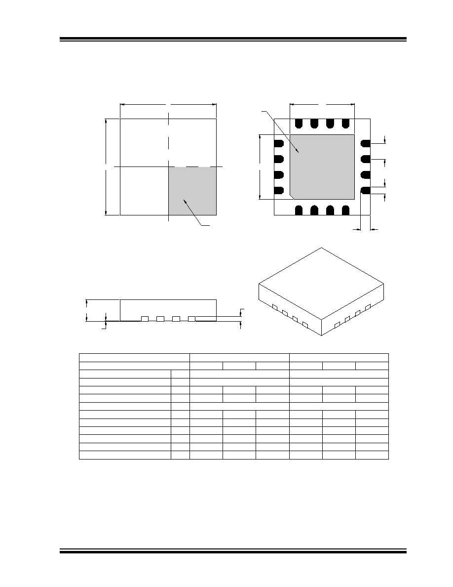
16-Lead Plastic Quad Flat No Lead Package (ML) 4x4x0.9 mm Body (QFN) � Saw Singulated
2
1
n
D
E
E1
D1
e
b
L
A
A1
A3
EXPOSED
METAL
PAD
OPTIONAL
INDEX
AREA
Contact Width
*Controlling Parameter
Drawing No. C04-127
Notes:
JEDEC equivalent: MO-220
b
.010
.012
.014
0.25
0.30
0.35
Pitch
Number of Pins
Overall Width
Standoff
Overall Length
Overall Height
MAX
Units
Dimension Limits
A1
D
E
n
e
A
.000
INCHES
.026 BSC
MIN
16
NOM
MAX
.002
0.00
4.00
MILLIMETERS*
.039
MIN
16
0.65 BSC
NOM
0.05
1.00
0.90
.035
.001
0.02
Contact Length
L
.012
.016
.020
0.30
0.40
0.50
E2
D2
Exposed Pad Width
Exposed Pad Length
.100
.106
.110
2.55
2.70
2.80
.031
0.80
3.85
4.15
.163
.157
.152
.152
.157
4.00
.163
3.85
4.15
.100
.106
2.70
.110
2.55
2.80
Revised 04-24-05
Contact Thickness
A3
.008 REF
0.20 REF
TOP VIEW
BOTTOM VIEW

MCP73861/2
DS21893A-page 22
2004 Microchip Technology Inc.
NOTES:
2004 Microchip Technology Inc.
DS21893A-page 23
MCP73861/2
PRODUCT IDENTIFICATION SYSTEM
To order or obtain information, e.g., on pricing or delivery, refer to the factory or the listed sales office
.
Sales and Support
Device
MCP73861:
Single-cell charge controller with temperature
monitor
MCP73861T:
Single-cell charge controller with temperature
monitor, Tape and Reel
MCP73862:
Dual series cells charge controller with
temperature monitor
MCP73862T:
Dual series cells charge controller with
temperature monitor, Tape and Reel
Temperature Range
I
= -40
�
C to +85
�
C (Industrial)
Package
ML
= Plastic Quad Flat No Lead, 4x4 mm Body (QFN),
16-lead
Lead Finish
G
= Matte Tin (Pure Sn)
PART NO.
X
XX
Package
Temperature
Range
Device
Examples:
a)
MCP73861T-I/MLG: Tape and Reel,
Single Cell Controller
b)
MCP73861-I/MLG: Single Cell Controller
a)
MCP73862T-I/MLG: Tape and Reel,
Dual Series Controller
b)
MCP73862-I/MLG: Dual Series Controller
Data Sheets
Products supported by a preliminary Data Sheet may have an errata sheet describing minor operational differences and
recommended workarounds. To determine if an errata sheet exists for a particular device, please contact one of the following:
1.
Your local Microchip sales office
2.
The Microchip Corporate Literature Center U.S. FAX: (480) 792-7277
3.
The Microchip Worldwide Site (www.microchip.com)
Please specify which device, revision of silicon and Data Sheet (include Literature #) you are using.
Customer Notification System
Register on our web site (www.microchip.com/cn) to receive the most current information on our products.

MCP73861/2
DS21893A-page 24
2004 Microchip Technology Inc.
NOTES:

2004 Microchip Technology Inc.
DS21893A-page 25
Information contained in this publication regarding device
applications and the like is intended through suggestion only
and may be superseded by updates. It is your responsibility to
ensure that your application meets with your specifications.
No representation or warranty is given and no liability is
assumed by Microchip Technology Incorporated with respect
to the accuracy or use of such information, or infringement of
patents or other intellectual property rights arising from such
use or otherwise. Use of Microchip's products as critical
components in life support systems is not authorized except
with express written approval by Microchip. No licenses are
conveyed, implicitly or otherwise, under any intellectual
property rights.
Trademarks
The Microchip name and logo, the Microchip logo, Accuron,
dsPIC, K
EE
L
OQ
, micro
ID
, MPLAB, PIC, PICmicro,
PICSTART, PRO MATE, PowerSmart, rfPIC, and
SmartShunt are registered trademarks of Microchip
Technology Incorporated in the U.S.A. and other countries.
AmpLab, FilterLab, MXDEV, MXLAB, PICMASTER, SEEVAL,
SmartSensor and The Embedded Control Solutions Company
are registered trademarks of Microchip Technology
Incorporated in the U.S.A.
Analog-for-the-Digital Age, Application Maestro, dsPICDEM,
dsPICDEM.net, dsPICworks, ECAN, ECONOMONITOR,
FanSense, FlexROM, fuzzyLAB, In-Circuit Serial
Programming, ICSP, ICEPIC, Migratable Memory, MPASM,
MPLIB, MPLINK, MPSIM, PICkit, PICDEM, PICDEM.net,
PICLAB, PICtail, PowerCal, PowerInfo, PowerMate,
PowerTool, rfLAB, rfPICDEM, Select Mode, Smart Serial,
SmartTel and Total Endurance are trademarks of Microchip
Technology Incorporated in the U.S.A. and other countries.
SQTP is a service mark of Microchip Technology Incorporated
in the U.S.A.
All other trademarks mentioned herein are property of their
respective companies.
� 2004, Microchip Technology Incorporated, Printed in the
U.S.A., All Rights Reserved.
Printed on recycled paper.
Note the following details of the code protection feature on Microchip devices:
�
Microchip products meet the specification contained in their particular Microchip Data Sheet.
�
Microchip believes that its family of products is one of the most secure families of its kind on the market today, when used in the
intended manner and under normal conditions.
�
There are dishonest and possibly illegal methods used to breach the code protection feature. All of these methods, to our
knowledge, require using the Microchip products in a manner outside the operating specifications contained in Microchip's Data
Sheets. Most likely, the person doing so is engaged in theft of intellectual property.
�
Microchip is willing to work with the customer who is concerned about the integrity of their code.
�
Neither Microchip nor any other semiconductor manufacturer can guarantee the security of their code. Code protection does not
mean that we are guaranteeing the product as "unbreakable."
Code protection is constantly evolving. We at Microchip are committed to continuously improving the code protection features of our
products. Attempts to break Microchip's code protection feature may be a violation of the Digital Millennium Copyright Act. If such acts
allow unauthorized access to your software or other copyrighted work, you may have a right to sue for relief under that Act.
Microchip received ISO/TS-16949:2002 quality system certification for
its worldwide headquarters, design and wafer fabrication facilities in
Chandler and Tempe, Arizona and Mountain View, California in
October 2003. The Company's quality system processes and
procedures are for its PICmicro
�
8-bit MCUs, K
EE
L
OQ
�
code hopping
devices, Serial EEPROMs, microperipherals, nonvolatile memory and
analog products. In addition, Microchip's quality system for the design
and manufacture of development systems is ISO 9001:2000 certified.

DS21893A-page 26
2004 Microchip Technology Inc.
AMERICAS
Corporate Office
2355 West Chandler Blvd.
Chandler, AZ 85224-6199
Tel: 480-792-7200
Fax: 480-792-7277
Technical Support: 480-792-7627
Web Address: www.microchip.com
Atlanta
3780 Mansell Road, Suite 130
Alpharetta, GA 30022
Tel: 770-640-0034
Fax: 770-640-0307
Boston
2 Lan Drive, Suite 120
Westford, MA 01886
Tel: 978-692-3848
Fax: 978-692-3821
Chicago
333 Pierce Road, Suite 180
Itasca, IL 60143
Tel: 630-285-0071
Fax: 630-285-0075
Dallas
4570 Westgrove Drive, Suite 160
Addison, TX 75001
Tel: 972-818-7423
Fax: 972-818-2924
Detroit
Tri-Atria Office Building
32255 Northwestern Highway, Suite 190
Farmington Hills, MI 48334
Tel: 248-538-2250
Fax: 248-538-2260
Kokomo
2767 S. Albright Road
Kokomo, IN 46902
Tel: 765-864-8360
Fax: 765-864-8387
Los Angeles
18201 Von Karman, Suite 1090
Irvine, CA 92612
Tel: 949-263-1888
Fax: 949-263-1338
San Jose
1300 Terra Bella Avenue
Mountain View, CA 94043
Tel: 650-215-1444
Fax: 650-961-0286
Toronto
6285 Northam Drive, Suite 108
Mississauga, Ontario L4V 1X5, Canada
Tel: 905-673-0699
Fax: 905-673-6509
ASIA/PACIFIC
Australia
Suite 22, 41 Rawson Street
Epping 2121, NSW
Australia
Tel: 61-2-9868-6733
Fax: 61-2-9868-6755
China - Beijing
Unit 706B
Wan Tai Bei Hai Bldg.
No. 6 Chaoyangmen Bei Str.
Beijing, 100027, China
Tel: 86-10-85282100
Fax: 86-10-85282104
China - Chengdu
Rm. 2401-2402, 24th Floor,
Ming Xing Financial Tower
No. 88 TIDU Street
Chengdu 610016, China
Tel: 86-28-86766200
Fax: 86-28-86766599
China - Fuzhou
Unit 28F, World Trade Plaza
No. 71 Wusi Road
Fuzhou 350001, China
Tel: 86-591-7503506
Fax: 86-591-7503521
China - Hong Kong SAR
Unit 901-6, Tower 2, Metroplaza
223 Hing Fong Road
Kwai Fong, N.T., Hong Kong
Tel: 852-2401-1200
Fax: 852-2401-3431
China - Shanghai
Room 701, Bldg. B
Far East International Plaza
No. 317 Xian Xia Road
Shanghai, 200051
Tel: 86-21-6275-5700
Fax: 86-21-6275-5060
China - Shenzhen
Rm. 1812, 18/F, Building A, United Plaza
No. 5022 Binhe Road, Futian District
Shenzhen 518033, China
Tel: 86-755-82901380
Fax: 86-755-8295-1393
China - Shunde
Room 401, Hongjian Building, No. 2
Fengxiangnan Road, Ronggui Town, Shunde
District, Foshan City, Guangdong 528303, China
Tel: 86-757-28395507 Fax: 86-757-28395571
China - Qingdao
Rm. B505A, Fullhope Plaza,
No. 12 Hong Kong Central Rd.
Qingdao 266071, China
Tel: 86-532-5027355 Fax: 86-532-5027205
India
Divyasree Chambers
1 Floor, Wing A (A3/A4)
No. 11, O'Shaugnessey Road
Bangalore, 560 025, India
Tel: 91-80-22290061 Fax: 91-80-22290062
Japan
Benex S-1 6F
3-18-20, Shinyokohama
Kohoku-Ku, Yokohama-shi
Kanagawa, 222-0033, Japan
Tel: 81-45-471- 6166 Fax: 81-45-471-6122
Korea
168-1, Youngbo Bldg. 3 Floor
Samsung-Dong, Kangnam-Ku
Seoul, Korea 135-882
Tel: 82-2-554-7200 Fax: 82-2-558-5932 or
82-2-558-5934
Singapore
200 Middle Road
#07-02 Prime Centre
Singapore, 188980
Tel: 65-6334-8870 Fax: 65-6334-8850
Taiwan
Kaohsiung Branch
30F - 1 No. 8
Min Chuan 2nd Road
Kaohsiung 806, Taiwan
Tel: 886-7-536-4818
Fax: 886-7-536-4803
Taiwan
Taiwan Branch
11F-3, No. 207
Tung Hua North Road
Taipei, 105, Taiwan
Tel: 886-2-2717-7175 Fax: 886-2-2545-0139
EUROPE
Austria
Durisolstrasse 2
A-4600 Wels
Austria
Tel: 43-7242-2244-399
Fax: 43-7242-2244-393
Denmark
Regus Business Centre
Lautrup hoj 1-3
Ballerup DK-2750 Denmark
Tel: 45-4420-9895 Fax: 45-4420-9910
France
Parc d'Activite du Moulin de Massy
43 Rue du Saule Trapu
Batiment A - ler Etage
91300 Massy, France
Tel: 33-1-69-53-63-20
Fax: 33-1-69-30-90-79
Germany
Steinheilstrasse 10
D-85737 Ismaning, Germany
Tel: 49-89-627-144-0
Fax: 49-89-627-144-44
Italy
Via Quasimodo, 12
20025 Legnano (MI)
Milan, Italy
Tel: 39-0331-742611
Fax: 39-0331-466781
Netherlands
Waegenburghtplein 4
NL-5152 JR, Drunen, Netherlands
Tel: 31-416-690399
Fax: 31-416-690340
United Kingdom
505 Eskdale Road
Winnersh Triangle
Wokingham
Berkshire, England RG41 5TU
Tel: 44-118-921-5869
Fax: 44-118-921-5820
05/28/04
W
ORLDWIDE
S
ALES
AND
S
ERVICE