1
The SY89529L is a high-speed, precision PLL-based
LVPECL clock synthesizer with spread-spectrum
modulation control. With an external 16.66MHz crystal
providing a reference frequency to the internal PLL, the
differential PECL output frequency will be 200MHz with
< 30ps (20ps typ.) peak-to-peak, cycle-to-cycle output
jitter. The SY89529L spread-spectrum mode operates with
a 30kHz triangle modulation with 0.5% down-spread (+0.0%/
ş0.5%). When spread-spectrum is activated, the output
signal is modulated which spreads the peak amplitudes
and, thus, decreases EMI (Electro-Magnetic Interference).
FEATURES
DESCRIPTION
Rev.: D
Amendment: /0
Issue Date:
April 2002
ClockWorksTM
SY89529L
3.3V 200MHz PRECISION
SPREAD-SPECTRUM
CLOCK SYNTHESIZER
s
Low voltage, 3.3V power supply operation
s
200MHz precision LVPECL output from a low cost
16.66MHz crystal
s
0.5% spread-spectrum modulation control
s
> 7dB reduction in EMI with spread-spectrum
modulation
s
LVTTL/LVCMOS compatible control inputs
s
interfaces directly to a crystal
s
Precision PLL architecture ensures < 30ps
peak-to-peak, cycle-to-cycle output jitter
s
48%-to-52% precision duty cycle is ideal for double-
data-rate clocking applications
s
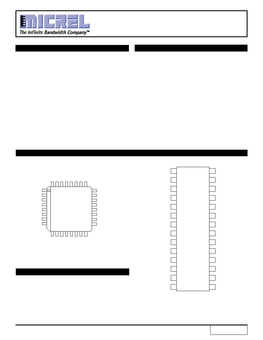
Available in low cost 32-pin TQFP and 28-pin SOIC
packages
PIN CONFIGURATION
APPLICATIONS
s
High-speed synchronous systems
s
CPU clock
s
Multi-processor workstations and servers
s
Networking
VCC_ANALOG
XTAL1
NC
NC
NC
LOOP_REF
GND_ANALOG
LOOP_FILTER
VCC1
NC
NC
NC
NC
XT
AL2
NC
NC
NC
NC
NC
NC
SSC CONTROL(1)
NC
SSC CONTROL(0)
FOUT
VCC_OUT
TEST INPUT
GND OUTPUT
VCC_TTL
GND_TTL
NC
NC
/FOUT
TQFP
TOP VIEW
T32-1*
1
2
3
4
5
6
7
8
32 31 30
29
28 27 26
25
24
23
22
21
20
19
18
17
16
15
14
13
12
11
10
9
1
NC
NC
VCC1
NC
XTAL2
NC
XTAL1
NC
LOOP_REF
NC
LOOP_FILTER
NC
VCC_ANALOG
NC
GND_ANALOG
NC
NC
NC
NC
SSC CONTROL(0)
VCC_OUT
SSC CONTROL(1)
FOUT
GND_TTL
/FOUT
TEST INPUT
GND OUTPUT
VCC_TTL
28
2
27
3
26
4
25
5
24
6
23
7
22
8
21
9
20
10
19
11
18
12
17
13
16
14
15
TOP VIEW
SOIC
Z28-1
*Contact factory for availability.

2
ClockWorksTM
SY89529L
Micrel
BLOCK DIAGRAM
PHASE DETECTOR
VCO
¸
M
¸
4
OSC
/FOUT
FOUT
16.66MHz
XTAL
¸
N
SSC CTL
30-33kHz
Down Spread
0.5%
Spread
Spectrum
Control
Diagnostic
Control
2
Control
TEST INPUT
PLL
INTERFACE
LOGIC
1
TEST
200MHz
Commands
Operational Modes
SSC_CTL
(1:0)
VCO
SSC
FOUT, /FOUT
0 0
--
--
--
Reserved (Supplier Internal Test Mode)
0 1
Run
Run
200MHz
Default SSC; Modulation Factor = 0.5%
1 0
Stop
Stop
TEST_I/O
Diagnostic Mode; (1MHz
TEST INPUT
200MHz)
1 1
Run
Stop
200MHz
No Spread-Spectrum
Table 1. SY89529L Control/Operational Modes

3
ClockWorksTM
SY89529L
Micrel
Input/Output Pins
Pin Number
Pin Number
Pin Name
I/O
Pin Function
SOIC
TQFP
25,26
8, 9
XTAL1, XTAL2
Analog
These pins form an oscillator when connected to an external
Inputs
crystal. Either series or parallel-resonant crystals are
acceptable. Connect directly to the device.
10, 11
23, 24
SSC Control (0:1)
LVTTL
LVTTL-compatible spread-spectrum control pins. Data on
Inputs
control pins maintain device control. For spread-spectrum
operation, leave SSC_0 and SSC_1 pins floating (default is
spread ON). To reconfigure the device, simply change the
SSC and the device will respond dynamically.
SSC_0 = 24k
pullup. SSC_1 = 24k
pulldown
16, 17
30, 31
FOUT, /FOUT
Differential
Differential, LVPECL clock outputs. These outputs must be
terminated to V
CC
ş2V. (see Figure 6)
23
6
LOOP_FILTER
Analog I/O
Used for the R//C PLL loop filter. (see Figure 2.)
24
7
LOOP_REF
Analog I/O
Provides the reference voltage for the PLL. (see Figure 2).
13
27
TEST INPUT
LVTTL
Pin is used for test and debug purposes. Is intended to be
Inputs
left floating in production environment. Programmed as
input in PLL-bypass mode. Pin includes an internal 24k
pullup resistor.
Power Supply Pins
Pin Number
Pin Number
Pin Name
I/O
Pin Function
SOIC
TQFP
14, 27
10, 28
V
CC1
, V
CC_TTL
Logic
3.3V LVTTL core logic power-supply pins. Connect each
Power
pin directly to the logic-supply plane and use proper
bypassing at each pin as close to the pin as possible; Ferrite
bead in parallel with 1
Á
F//0.01
Á
F capacitors. (see Figure 5
for typical bypass circuit.)
22
5
ANALOG_ V
CC
PLL
3.3V PLL core supply pin. Must be a noise free supply.
Power
Bypass as close to the pin as possible; ferrite bead in
parallel with 1
Á
F//0.01
Á
F capacitors.
(
see Figure 5 for
typical bypass circuit.)
18
32
V
CC_OUT
Output
This is the positive power supply reference for the LVPECL
Power
outputs (FOUT and /FOUT). See Figure 5 for typical bypass
circuit.
12
26
GND_TTL
Logic
This is the ground pin for for the TTL control logic. Normally
connected to the logic ground.
21
4
GND_ANALOG
Analog
This is the ground pin for the PLL Core. Normally connected
GND
to a quiet, noise-free ground plane for low jitter perfomance.
15
29
GND_OUTPUT
Output
Ground for differential outputs. Normally connected to the
GND
logic ground plane.
No Connect Pins
Pin Number
Pin Number
Pin Name
I/O
Pin Function
SOIC
TQFP
1, 2, 3, 4, 5
1, 2, 3, 11, 12, 13
NC
No
Pins are high-impedance, low leakage and are not used by
6, 7, 8, 9, 19
14, 15, 16, 17, 18
Connect
internal circuits of the device. These pins are intended to be
20, 28
19, 20, 21, 22, 25
left floating in production.
PIN DESCRIPTIONS
4
ClockWorksTM
SY89529L
Micrel
FUNCTIONAL DESCRIPTION AND TEST MODES
Introduction
The SY89529L supports three operational modes, as shown
in Table 1, page 2. The three modes are spread-spectrum
clocking (SSC), non-spread-spectrum clock, and a test mode
dynamically controlled with the SSC_Control pins. Unlike
other synthesizers, the SY89529L can change spread-
spectrum operation on the fly.
In SSC mode, the output clock is modulated (30KHz,
triangle waveform) in order to achieve a reduction in EMI. In
the PLL-bypass test mode, the PLL is disconnected as the
source to the differential output, thus allowing an external
source to be connected to the TEST INPUT pin. This is useful
for in-circuit testing by enabling the differential output to be
driven at a lower frequency.
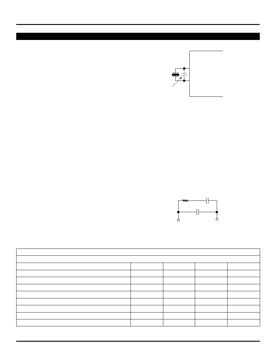
Crystal Input and Oscillator Interface
The SY89529L features a fully integrated on-board oscillator
to minimize system implementation costs. The oscillator is a
series resonant, multivibrator type design, and thus, a series-
resonant crystal is preferred, but not required.
A parallel-resonant crystal can be used with the SY89529L
with only a minor error in the desired frequency. A parallel-
resonant mode crystal used in a series resonant circuit will
exhibit a frequency of oscillation a few hundred ppm lower
than specified, a few hundred ppm translates to KHz
inaccuracies. In a general computer application this level of
inaccuracy is immaterial.
As the oscillator is somewhat sensitive to loading on its
inputs, the user is advised to mount the crystal as close to the
SY89529L as possible to avoid any board level parasitics. In
addition, trace lengths should be matched. Figure 1 shows
how to interface with a crystal. Table 2 illustrates the crystal
specifications. If a start-up problem occurs, consider adding a
10pf capacitor across XTAL1 and XTAL2.
SY89529L
XTAL2
(Pin 26, SOIC)
XTAL1
(Pin 25, SOIC)
XTAL
16.666MHz
Quartz Crystal Selection:
(1) Raltron Series Resonant: AS-16.666-S-SMD-T-MI
(2) Raltron Parallel Resonant: AS-16.666-18-SMD-T-MI
Optional
Figure 1. Crystal Interface
Loop Filter Design
The filter for any Phase Locked Loop (PLL) based device
deserves special attention. SY89529L provides filter pins for
an external filter. A simple three-component passive filter is
required for achieving ultra low jitter. Figure 2 shows the
recommended three-components. Due to the differential
design, the filter is connected between LOOP_FILTER and
LOOP_REF pins. With this configuration, extremely high
supply noise rejection is achieved. It is important that the filter
circuit and filter pins be isolated from any non-common mode
coupling plane.
1000pF
Loop
Filter
Loop
Reference
560
0.47
Á
F
Figure 2. External Loop Filter Connection
Table 2. Quartz Crystal Oscillator Specifications
Output Frequency: 16.666MHz
Mode of Oscillation: Fundamental
Min.
Typ.
Max.
Unit
Frequency Tolerance @25
░
C
--
▒
30
▒
50
ppm
Frequency Stability over 0
░
C to 70
░
C
--
▒
50
▒
100
ppm
Operating Temperature Range
ş20
--
+70
░
C
Storage Temperature Range
ş55
--
+125
░
C
Aging (per yr/1st 3yrs)
--
--
▒
5
ppm
Load Capacitance
--
18 (or series)
--
pF
Equivalent Series Resistance (ESR)
--
--
50
Drive Level
--
100
--
Á
W

5
ClockWorksTM
SY89529L
Micrel
Spread Spectrum
Spread-spectrum clocking is a frequency modulation
technique for EMI reduction. When spread-spectrum is
enabled, a 30kHz triangle waveform is used with 0.5% down-
spread (+0.0%/ş0.5%) from the nominal 200MHz clock
frequency. An example of a triangle frequency modulation
profile is shown in the figure 3 below. The ramp profile can be
expressed as:
Ě Fnom = Nominal Clock Frequency in Spread OFF mode
(200MHz with 16.66MHz IN)
Ě Fm = Nominal Modulation Frequency (30kHz)
Ě
= Modulation Factor (0.5% down spread)
1
2
0
1
2
1
2
1
2
1
-
(
)
+
Î Î
Î
< <
+
(
)
Î Î
Î
< <
fnom
fm
fnom
t when
t
fm
fnom
fm
fnom
t when
fm
t
fm
,
ş
0.5/fm
1/fm
fnom
(1ş
) fnom
t
Figure 3. Triangle Frequency Modulation
The SY89529L triangle modulation frequency deviation (
)
will not exceed 0.6% down-spread from the nominal clock
frequency (+0.0%/ş0.5%). An example of the amount of down
spread relative to the nominal clock frequency can be seen in
the frequency domain, as shown in Figure 4. The ratio of this
width to the fundamental frequency is typically 0.5%, and will
not exceed 0.6%. The resulting spectral reduction will be
greater than 7dB, as shown in Figure 5. It is important to note
the SY89529L 7dB minimum spectral reduction is the
component-specific EMI reduction, and will not necessarily be
the same as the system EMI reduction.
200MHz Clock Output in Frequency Domain
(A) Spread-Spectrum OFF
(B) Spread-Spectrum ON
TIME (400Ás/div.)
R = 560
C1 = 1000pF
C2 = 0.47
Á
F
V
CC
= 3.3V
T
A
= 25íC
Figure 5. 200MHz Clock Output in Frequency Domain
Figure 4. 0.38% Modulation,
32.7KHz Modulation Frequency