
May 13, 2004
1
M9999-051304
MICRF505
Micrel
MICRF505
868MHz and 915MHz ISM Band Transceiver
General Description
The MICRF505 is a true single chip, frequency shift keying
(FSK) transceiver intended for use in half-duplex, bidirec-
tional RF links. The multi-channeled FSK transceiver is
intended for UHF radio equipment in compliance with the
North American Federal Communications Commission (FCC)
part 15.247 and 249, as well as the European Telecommuni-
cation Standard Institute (ETSI) specification, EN300 220.
The transmitter consists of a PLL frequency synthesizer and
a power amplifier. The frequency synthesizer consists of a
voltage-controlled oscillator (VCO), a crystal oscillator, dual
modulus prescaler, programmable frequency dividers, and a
phase-detector. The loop-filter is external for flexibility and
can be a simple passive circuit. The output power of the
power amplifier can be programmed to seven levels. A lock-
detect circuit detects when the PLL is in lock. In receive mode,
the PLL synthesizer generates the local oscillator (LO) signal.
The N, M , and A values that give the LO frequency are stored
in the N0, M0, and A0 registers.
The receiver is a zero intermediate frequency (IF) type which
makes channel filtering possible with low-power, integrated
low-pass filters. The receiver consists of a low noise amplifier
(LNA) that drives a quadrature mixer pair. The mixer outputs
feed two identical signal channels in phase quadrature. Each
channel includes a pre-amplifier, a third order Sallen-Key RC
low-pass filter that protects the following switched-capacitor
filter from strong adjacent channel signals, and a limiter. The
main channel filter is a switched-capacitor implementation of
a six-pole elliptic low pass filter. The cut-off frequency of the
Sallen-Key RC filter can be programmed to four different
frequencies: 100kHz, 150kHz, 230kHz, and 340kHz. The I
and Q channel outputs are demodulated and produce a
digital data output. The demodulator detects the relative
phase of the I and the Q channel signal. If the I channel signal
lags behind the Q channel, the FSK tone frequency is above
the LO frequency (data `1'). If the I channel leads the Q
channel, the FSK tone is below the LO frequency (data `0').
The output of the receiver is available on the DataIXO pin. A
receive signal strength indicator (RSSI) circuit indicates the
received signal level. All support documentation can be
found on Micrel's web site at www.micrel.com.
Features
Ě True single chip transceiver
Ě Digital bit synchronizer
Ě Received signal strength indicator (RSSI)
Ě RX and TX power management
Ě Power down function
Ě Reference crystal tuning capabilities
Ě Baseband shaping
Ě Three-wire programmable serial interface
Ě Register read back function
Applications
Ě Telemetry
Ě Remote metering
Ě Wireless controller
Ě Remote data repeater
Ě Remote control systems
Ě Wireless modem
Ě Wireless security system
Ordering Information
Part Number
Junction Temp. Range
Package
MICRF505BML
ş40
C to +85C
32-Pin MLFTM
Micrel, Inc. Ě 1849 Fortune Drive Ě San Jose, CA 95131 Ě USA Ě tel + 1 (408) 944-0800 Ě fax + 1 (408) 474-1000 Ě http://www.micrel.com
Micro
LeadFrame and MLF are trademarks of Amkor Technology, Inc.
MICRF505
Micrel
M9999-051304
2
May 13, 2004
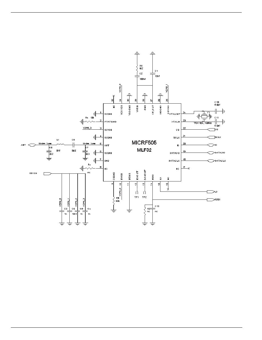
Typical Application
May 13, 2004
3
M9999-051304
MICRF505
Micrel
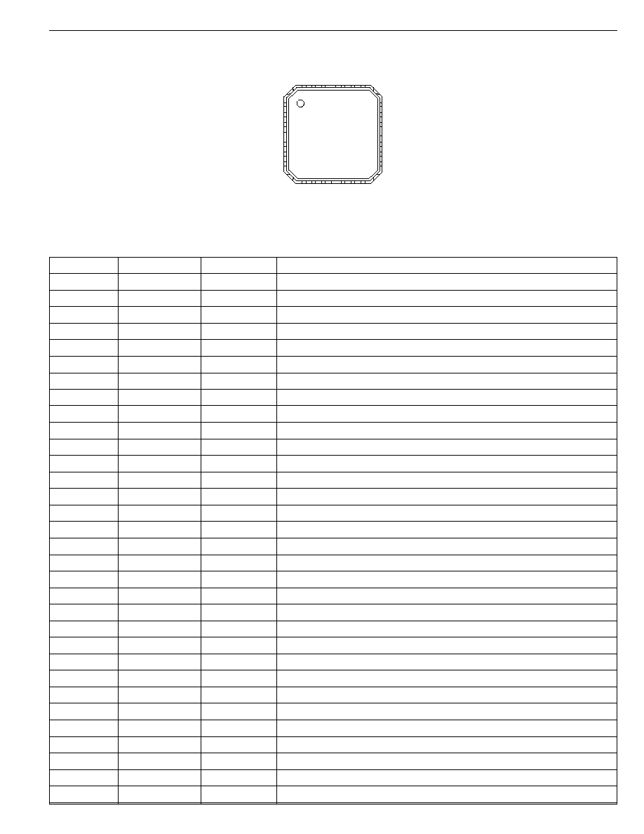
Pin Configuration
32-Pin MLFTM
Pin Description
Pin Number
Pin Name
Type
Pin Function
1
RFGND
LNA and PA ground.
2
PTATBIAS
O
Connection for bias resistor.
3
RFVDD
LNA and PA power supply.
4
RFGND
LNA and PA ground.
5
ANT
I/O
Antenna In/Output
6
RFGND
LNA and PA ground.
7
RFGND
LNA and PA ground.
8
NC
No connect.
9
CIBIAS
O
Connection for bias resistor.
10
IFVDD
IF/mixer power supply.
11
IFGND
IF/mixer ground.
12
ICHOUT
O
Test pin.
13
QCHOUT
O
Test pin.
14
RSSI
O
Received signal strength indicator.
15
LD
O
PLL lock detect.
16
NC
No connect.
17
NC
No connect.
18
DATACLK
O
RX/TX data clock output.
19
DATAIXO
I/O
RX/TX data input/output.
20
IO
I/O
3-wire interface data in/output
21
SCLK
I
3-wire interface serial clock.
22
CS
I
3-wire interface chip select.
23
XTALIN
I
Crystal oscillator input.
24
XTALOUT
O
Crystal oscillator output.
25
DIGVDD
Digital power supply.
26
DIGGND
Digital ground.
27
CPOUT
O
PLL charge pump output.
28
GND
Substrate ground.
29
VARIN
I
VCO varactor input.
30
VCOGND
VCO ground.
31
VCOVDD
VCO power supply.
32
NC
No connect.
1
2
3
4
5
6
7
8
24
23
22
21
20
19
18
17
9 10 11 12 13 14 15 16
32 3130 29 28 27 26 25
MICRF505
32-pin
MLF
RFGND
PTA
RFVDD
RFGND
ANT
RFGND
GND
NC
XTALOUT
XTALIN
CS
SCLK
IO
DATAIXO
DATACLK
NC
GND
VA
R
I
N
VCOGND
VCOVD
NC
CPOUT
DIGGND
DIGVDD
QCHOUT
ICHOUT
IFGND
IFVDD
CIBIAS
RSSI
LD
NC

MICRF505
Micrel
M9999-051304
4
May 13, 2004
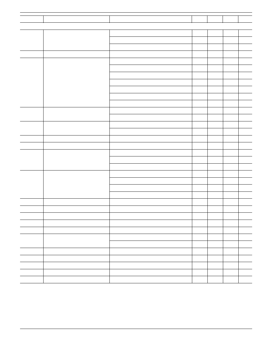
Absolute Maximum Ratings
(1)
Supply Voltage (V
DD
) ................................................. +3.3V
Voltage on any pin (GND = 0V) ................. ş0.3V to 2.7V
Lead Temperature (soldering, 4 sec.) ...................... TBD
C
Storage Temperature (T
S
) ....................... ş55
C to +150C
ESD Rating
(3) ...............................................................................
2kV
Operating Ratings
(2)
Supply Voltage (V
IN
) ................................... +2.0V to +2.5V
RF Frequencies ................................... 850MHz to 950MHz
Data Rate (NRZ) .............................................. < 200kBaud
Ambient Temperature (T
A
) ......................... ş40
C to +85C
Package Thermal Resistance
MLFTM
(q
JA
) multi-layer board .......................... 41.7
C/W
Electrical Characteristics
(4)
f
RF
= 915MHz, Data-rate = 125kbps, Modulation type = closed-loop VCO modulation, V
DD
= 2.5V; T
A
= 25
C, bold values indicate
ş40
C ú T
A
ú +85C; unless noted.
Symbol
Parameter
Condition
Min
Typ
Max
Units
RF Frequency Operating Range
850
950
MHz
Power Supply
2.0
2.5
V
Power Down Current
0.3
mA
Standby Current
280
mA
VCO and PLL Section
Reference Frequency
4
40
MHz
PLL Lock Time
915MHz to 915.5MHz
0.5
ms
3kHz bandwidth
902MHz to 927MHz
1.7
ms
20kHz bandwidth
0.3
ms
Switch Time
Rx ş Tx
0.6
ms
3kHz loop bandwidth
Tx ş Rx
0.6
ms
Standby Rx
1.1
ms
Standby Tx
1.2
ms
Crystal Oscillator Start-Up Time
16MHz, 9pF load, 5.6pF loading capacitors
1.2
ms
Charge Pump Current
VCP
OUT
= 1.1V, CP_HI = 0
125
mA
VCP
OUT
= 1.1V, CP_HI = 1
500
mA
Charge Pump Tolerance
20
%
Transmit Section
Output Power
R
LOAD
= 50
W, Pa2-0-111
10
dBm
R
LOAD
= 50
W, Pa2-0-001
ş8
dBm
Output Power Tolerance
Over temperature range
2
dB
Over power supply range
3
dB
Tx Current Consumption
R
LOAD
= 50
W, Pa2-0-111
28
mA
R
LOAD
= 50
W, Pa2-0-001
14
mA
Tx Current Consumption Variation
10dBm
2.5
mA
Binary FSK Frequency Separation
(5)
bitrate = 200kbps
20
500
kHz
Data Rate
(5)
VCO modulation
20
200
kbps
Occupid bandwidth
20kbps,
b = 2, 20dBc
kHz
125kbps,
b = 2, 20dBc
kHz
200kbps,
b = 2, 20dBc
kHz
2nd Harmonic
ş25
dBm
3rd Harmonic
ş15
dBm
Spurious Emission < 1GHz
(5)
< ş54
dBm
Spurious Emission < 1GHz
(5)
< ş30
dBm
May 13, 2004
5
M9999-051304
MICRF505
Micrel
Symbol
Parameter
Condition
Min
Typ
Max
Units
Receive Section
Rx Current Consumption
13.5
mA
LNA bypass
11.5
mA
Switch cap filter bypass with LNA
11.5
mA
Rx Current Consumption Variation
Over temperature
4
mA
Receiver Sensitivity
2.4kbps,
b = 16
ş111
dBm
4.8kbps,
b = 16
ş109
dBm
19.2kbps,
b = 4
ş105
dBm
38.4kbps,
b = 4
ş103
dBm
76.8kbps,
b = 2
ş101
dBm
125kbps,
b = 2
ş99
dBm
200kbps,
b = 2
ş97
dBm
Receiver Maximum Input Power
125kbps, 125kHz deviation
ş12
dBm
20kbps, 20kHz deviation
ş20
dBm
Receiver Sensitivity Tolerance
Over temperature
4
dB
Over power supply range
1
dB
Receiver Bandwidth
50
340
kHz
Co-Channel Rejection
dB
Adjacent Channel Rejection
200kHz spacing
500kHz spacing
1MHz spacing
Blocking
▒1MHz
42
dB
▒2MHz
47
dB
▒5MHz
38
dB
▒10MHz
41
dB
Noise Figure, Cascade
tbd
dB
1dB Compression
ş35
dB
Input IP3
2 tones with 1MHz separation
ş25
dBm
Input IP2
dBm
LO Leakage
ş90
dBm
Spurious Emission
< 1GHz
ş54
dBm
> 1GHz
ş54
dBm
Input Impedance
(5)
~50
W
Input Reflection (s11)
(5)
ş20
ş15
dB
RSSI Dynamic Range
50
dB
RSSI Output Voltage
Pin = 100dBm
0.9
V
Pin = 60dBm
1.85
V