MIC59P50
Micrel
7-58
October 1998
IN
Circuitry below dashed line is
included in each of the 8 channels.
STROBE
VDD
2.2R
1.25V
R
+
UVLO
CLEAR
ENABLE/RESET
ISHUTDOWN
COMMON
S
R
Q
R1
70k
R2
3k
VEE
OUTPUT
THERMAL
SHUTDOWN
IREF
IOUT / N
FLAG
+
General Description
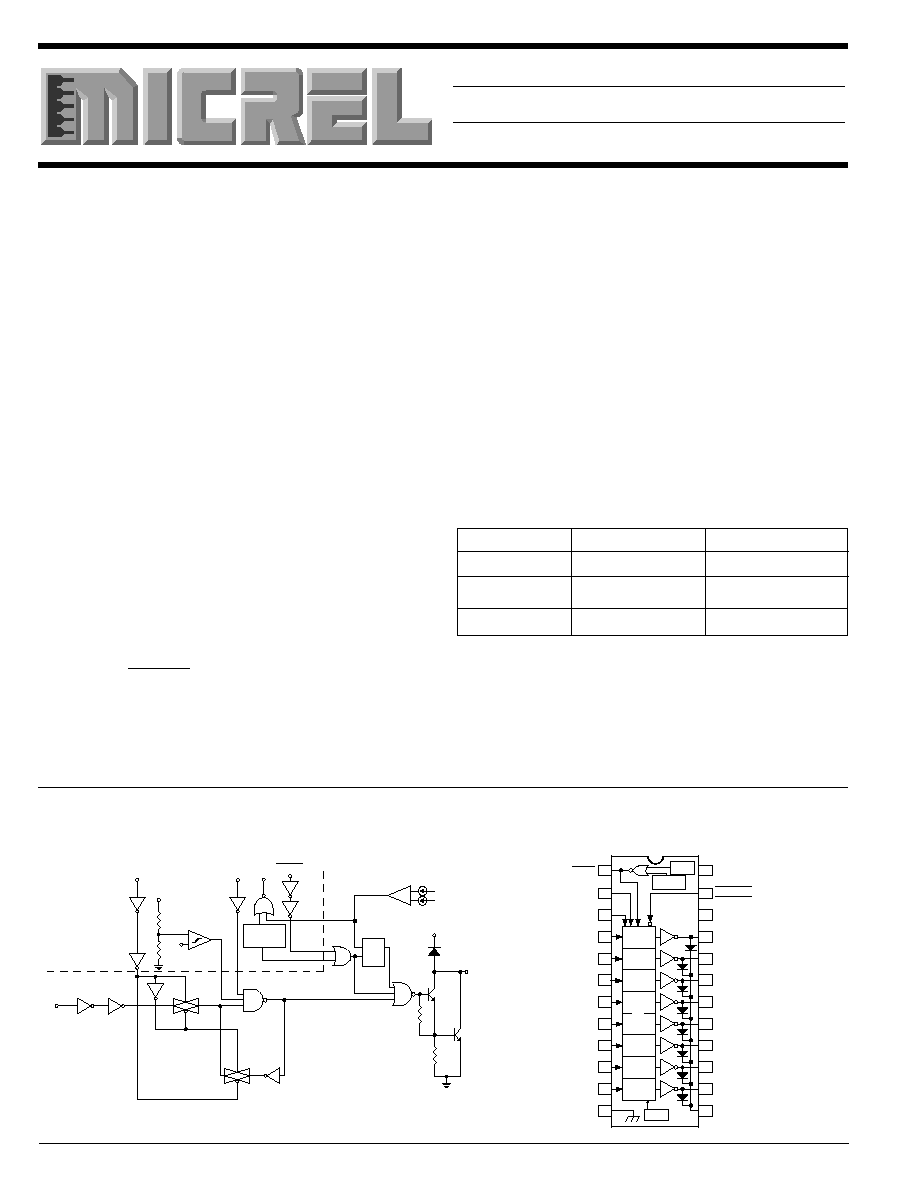
The MIC59P50 parallel-input latched driver is a high-voltage
(80V), high-current (500mA) integrated circuit comprised of
eight CMOS data latches, a bipolar Darlington transistor
driver for each latch, and CMOS control circuitry for the
common CLEAR, STROBE, and OUTPUT ENABLE func-
tions. Similar to the MIC5801, additional protection circuitry
supplied on this device includes thermal shutdown, under
voltage lockout (UVLO), and over-current shutdown.
The bipolar/MOS combination provides an extremely low-
power latch with maximum interface flexibility. The MIC59P50
has open-collector outputs capable of sinking 500mA and
integral diodes for inductive load transient suppression with
a minimum output breakdown voltage rating of 80V above V
EE
(50V sustaining). The drivers can be operated with a split
supply, where the negative supply is down to 20V and may
be paralleled for higher load current capability.
With a 5V logic supply, the MIC59P50 will typically operate at
better than 5MHz. With a 12V logic supply, significantly
higher speeds are obtained. The CMOS inputs are compat-
ible with standard CMOS, PMOS, and NMOS circuits. TTL
circuits may require pull-up resistors.
Each of these eight outputs has an independent over-current
shutdown at 500 mA. Upon current shutdown, the affected
channel will turn OFF and the flag will go low until V
DD
is
cycled or the ENABLE/RESET pin is pulsed high. Current
pulses less than 2
µ
s will not activate over-current shutdown.
Temperatures above 165
°
C will shut down the device and
activate the open collector FLAG output at pin 1. The UVLO
circuit disables the outputs at low V
DD
; hysteresis of 0.5V is
provided.
Ordering Information
Part Number
Temperature Range
Package
MIC59P50BN
40
°
C to +85
°
C
24-Pin Plastic DIP*
MIC59P50BV
40
°
C to +85
°
C
28-Pin PLCC
MIC59P50BWM
40
°
C to +85
°
C
24-Pin Wide SOIC
Features
· 4.4 MHz Minimum Data Input Rate
· High-Voltage, High-Current Outputs
· Per-Output Over-Current Shutdown (500mA Typical)
· Undervoltage Lockout
· Thermal Shutdown
· Output Fault Flag
· Output Transient Protection Diodes
· CMOS, PMOS, NMOS, and TTL Compatible Inputs
· Internal Pull-Down Resistors
· Low-Power CMOS Latches
· Single or Split Supply Operation
Functional Diagram
Pin Configuration
(DIP and SOIC)
* 300-mil "skinny DIP"
MIC59P50
8-Bit Parallel-Input Protected Latched Driver
12
11
10
9
8
7
6
5
4
3
2
1
LATCHES
UVLO
ILIMIT
THERMAL
SHUTDOWN
13
14
15
16
17
18
19
20
21
22
23
24
VEE
IN 8
IN 7
IN 6
IN 5
IN 4
IN 3
IN 2
IN 1
CLEAR
FLAG
STROBE
VSS
ENABLE/RESET
VDD
OUT 1
OUT 2
OUT 3
OUT 4
OUT 5
OUT 6
OUT 7
OUT 8
COMMON
OUTPUT
October 1998
7-59
MIC59P50
Micrel
7
Pin Description
Pin
Name
Description
1
FLAG
Error Flag. Open Collector Output is Low upon Overcurrent Fault or
Overtemperature Fault. OUTPUT ENABLE/RESET must be pulled high to
reset the flag and fault condition.
2
CLEAR
Sets All Latches OFF (open).
3
STROBE
Input Strobe Pin. Loads output latches when High.
411
INPUT
Parallel Inputs, 1 through 8
12
V
EE
Output Ground (Substrate). Most negative voltage in the system connects
here.
13
COMMON
Transient suppression diodes cathode common pin.
1421
OUTPUT
Parallel Outputs, 8 through 1.
22
V
DD
Logic Positive Supply voltage.
23
OUTPUT ENABLE RESET
Output Enable Reset. When Low, Outputs are active. When High, outputs
are inactive and the Flag and outputs are reset from a fault condition. An
undervoltage condition emulates a high OE input.
24
V
SS
Logic reference (Ground) pin.
Absolute Maximum Ratings
T
A
= +25
°
C
Output Voltage (V
CE
) .................................................... 80V
Supply Voltage (V
DD
) .................................................... 15V
(V
DD
V
EE
) ............................................................... 25V
Input Voltage (V
IN
) ............................... 0.3V to V
DD
+0.3V
Continuous Collector Current (I
C
) ............................ 500mA
Protected Current ............................................ 1.5A, Note 1
Power Dissipation (P
D
)
Plastic DIP (N) ......................................................... 2.4W
Derate above T
A
= +25
°
C ............................ 24mW/
°
C
PLCC (V) ................................................................. 1.6W
Derate above T
A
= +25
°
C ............................ 16mW/
°
C
Wide SOIC (WM) .................................................... 1.4W
Derate above T
A
= +25
°
C ............................ 14mW/
°
C
Operating Temperature (T
A
)
Plastic DIP (N), PLCC (V), SOIC (WM) .. 40
°
C to +85
°
C
Storage Temperature (T
S
) ....................... 65
°
C to +150
°
C
Junction Temperature (T
J
) ...................................... +150
°
C
ESD ......................................................................... Note 2
Note 1:
Each channel. V
EE
connection must be designed to minimize
inductance and resistance.
Note 2:
Devices are input-static protected but can be damage by
extremely high static charges.
Typical Input
IN
DD
V
0
10
20
30
40
50
60
70
80
90
100
450
400
350
300
250
200
150
100
PERCENT DUTY CYCLE
ALLOW
ABLE COLLECT
OR CURRENT
I
N
mA
A
T
50
°
C
3
1 or 2
4
NUMBER OF OUTPUTS
CONDUCTING
SIMULTANEOUSLY
5
6
7
8
MIC59P50BN
Allowable Output Current
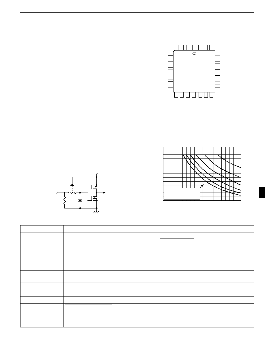
PLCC Pin Configuration
1
2
3
4
12
13
14
28
27
26
25
19
20
21
22
23
24
18
17
16
15
5
6
7
8
9
10
11
OUT 1
OUT 2
OUT 3
OUT 4
OUT 5
OUT 6
OUT 7
OUT 8
COMMON
NC
V
EE
IN 8
IN 7
IN 6
IN 5
IN 4
IN 3
IN 2
IN 1
STROBE
CLEAR
OE/RESET
V
DD
FLAG
NC
NC
V
EE
MIC59P50BV
V
SS

MIC59P50
Micrel
7-60
October 1998
Electrical Characteristics
V
DD
= 5V; T
A
= +25
°
C; unless noted.
Limits
Characteristic
Symbol
Test Conditions
Min.
Typ.
Max.
Units
Output Leakage Current
I
CEX
V
CE
= 80V, T
A
= +25
°
C
50
µ
A
V
CE
= 80V, T
A
= +70
°
C
100
Collector-Emitter
V
CE(SAT)
I
C
= 100 mA
0.9
1.1
V
Saturation Voltage
I
C
= 200 mA
1.1
1.3
I
C
= 350 mA
1.3
1.6
Input Voltage
V
IN(0)
1.0
V
V
IN(1)
V
DD
= 12V
10.5
V
DD
= 10V
8.5
V
DD
= 5.0V Note 3
3.5
Input Resistance
R
IN
V
DD
= 12V
50
200
k
V
DD
= 10V
50
300
V
DD
= 5.0V
50
600
Flag Output Current
I
OL
V
OL
= 0.4V
15
mA
Flag Output Leakage
I
OH
V
OH
= 12.0V
50
nA
Supply Current
I
DD(ON)
V
DD
= 12V, Outputs Open
3.3
4.5
mA
(One output
V
DD
= 10V, Outputs Open
3.1
4.5
active)
V
DD
= 5.0V, Outputs Open
2.4
3.6
I
DD(ON)
V
DD
= 12V, Outputs Open
6.4
10.0
mA
(All outputs
V
DD
= 10V, Outputs Open
6.0
9.0
active)
V
DD
= 5.0V, Outputs Open
4.7
7.5
I
DD(OFF)
V
DD
= 12V, Outputs Open, Inputs = 0V
3.0
4.5
mA
(Total)
V
DD
= 5.0V, Outputs Open, Inputs = 0V
2.2
3.6
Clamp Diode
I
R
V
R
= 80V, T
A
= +25
°
C
50
µ
A
Leakage Current
V
R
= 80V, T
A
= +70
°
C
100
Over-Current Threshold
I
LIM
Each Output
500
mA
Start-Up Voltage
V
SU
Note 4
3.5
4.0
4.5
V
Minimum Operating V
DD
V
DD MIN
3.0
3.5
4.0
V
Clamp Diode Forward Voltage
V
F
I
F
= 350 mA
1.7
2.0
V
Thermal Shutdown
165
°
C
Thermal Shutdown Hysteresis
10
NOTE 3:
Operation of these devices with standard TTL or DTL may require the use of appropriate pull-up resistors to insure a minimum logic "1".
NOTE 4:
Undervoltage lockout is guaranteed to release device at no more than 4.5V and disable the device at no less than 3.0V input logic voltage.
Truth Table
Output
OUT
N
IN
N
Strobe
Clear
Enable
t1
t
0
1
0
0
X
OFF
1
1
0
0
X
ON
X
X
1
X
X
OFF
X
X
X
1
X
OFF
X
0
0
0
ON
ON
X
0
0
0
OFF
OFF
X = Irrelevant
t1 = previous output state
t = present output state
Information present at an input is transferred to its latch when
the STROBE is high. A high CLEAR input will set all latches
to the output OFF condition regardless of the data or STROBE
input levels. A high OUTPUT ENABLE will set all outputs to
the off condition, regardless of any other input conditions.
When the OUTPUT ENABLE is low, the outputs depend on
the state of their respective latches. If current shutdown is
activated, the OUTPUT ENABLE must be pulsed high to
restore operation and reset the Flag. Over temperature
faults are not latched and require no reset pulse.

October 1998
7-61
MIC59P50
Micrel
7
CLEAR
F
STROBE
OUTPUT
ENABLE
IN
C
B
A
G
N
E
C
B
A
G
D
C
B
E
OUT N
Timing Conditions
(T
A
= +25
°
C, Logic Levels are V
DD
and V
SS
, V
DD
= 5V).
A.
Minimum data active time before strobe enabled (data set-up time) ...................................................................... 50 ns
B.
Minimum data active time after strobe disabled (data hold time) ............................................................................ 50 ns
C.
Minimum strobe pulse width .................................................................................................................................. 125 ns
D.
Typical time between strobe activation and output on to off transition .................................................................. 500 ns
E.
Typical time between strobe activation and output off to on transition .................................................................. 500 ns
F.
Minimum clear pulse width .................................................................................................................................... 300 ns
G.
Minimum data pulse width ..................................................................................................................................... 225 ns
0.6
0.7
0.8
0.9
1
1.1
1.2
1.3
1.4
1.5
1.6
50
0
50
100
150
SATURATION VOLTAGE (V)
TEMPERATURE (°C)
Output Saturation
Voltage vs. Temperature
I
L
= 350mA
V
DD
= 5V to 12V
I
L
= 100mA
0
1
2
3
4
5
6
50
0
50
100
150
SUPPLY CURRENT (mA)
TEMPERATURE (°C)
Supply Current
vs. Temperature
V
DD
= 5V
ALL OUTPUTS ON
ALL OUTPUTS OFF
0
1
2
3
4
5
6
7
0.4
0.5
0.6
0.7
0.8
0.9
CURRENT SHUTDOWN DELAY (µs)
OUTPUT CURRENT (A)
Current Shutdown
Delay vs. Output Current
V
DD
= 5V
V
DD
= 12V
0.35
0.40
0.45
0.50
0.55
0.60
50
0
50
100
150
SHUTDOWN THRESHOLD (A)
TEMPERATURE (°C)
V
DD
= 5V
V
DD
= 12V
Current Shutdown
Threshold vs. Temperature
0
1
2
3
4
5
6
7
8
50
0
50
100
150
SUPPLY CURRENT (mA)
TEMPERATURE (°C)
Supply Current
vs. Temperature
V
DD
= 12V
ALL OUTPUTS ON
ALL OUTPUTS OFF
100
120
140
160
180
200
220
240
260
5
6
7
8
9 10 11 12 13 14 15
OUTPUT DELAY (ns)
SUPPLY VOLTAGE (V)
Output Enable Delay
vs. Supply Voltage
T
D
OFF
T
D
ON
R
L
= 50
Typical Characteristic Curves

MIC59P50
Micrel
7-62
October 1998
Typical Applications
K1
K3
K2
K8
K7
K6
K5
K4
INPUT 1
INPUT 8
INPUT 7
INPUT 6
INPUT 5
INPUT 4
INPUT 3
INPUT 2
+24V
+5V
STROBE
0.1µF 22µF
+
FLAG
OUTPUT
+5V
10k
12
11
10
9
8
7
6
5
4
3
2
1
LATCHES
UVLO
ILIMIT
THERMAL
SHUTDOWN
13
14
15
16
17
18
19
20
21
22
23
24
MIC59P50 Protected Relay Driver