
1997
5-155
MIC5018
Micrel
5
MIC5018
IttyBittyTM High-Side MOSFET Driver
Preliminary Information
General Description
The MIC5018 IttyBittyTM high-side MOSFET driver is de-
signed to switch an N-channel enhancement-type MOSFET
from a TTL compatible control signal in high- or low-side
switch applications. This driver features the tiny 4-lead
SOT-143 package.
The MIC5018 is powered from a +2.7V to +9V supply and
features extremely low off-state supply current. An internal
charge pump drives the gate output higher than the driver
supply voltage and can sustain the gate voltage indefinitely.
An internal zener diode limits the gate-to-source voltage to a
safe level for standard N-channel MOSFETs.
In high-side configurations, the source voltage of the MOS-
FET approaches the supply voltage when switched on. To
keep the MOSFET turned on, the MIC5018's output drives
the MOSFET gate voltage higher than the supply voltage. In
a typical high-side configuration, the driver is powered from
the load supply voltage. Under some conditions, the MIC5018
and MOSFET can switch a load voltage that is slightly higher
than the driver supply voltage.
In a low-side configuration, the driver can control a MOSFET
that switches any voltage up to the rating of the MOSFET.
The gate output voltage is higher than the typical 3.3V or 5V
logic supply and can fully enhance a standard MOSFET.
The MIC5018 is available in the SOT-143 package and
is rated for ¡40
░
C to +85
░
C ambient temperature range.
Typical Applications
Features
À +2.7V to +9V operation
À 150
Á
A typical supply current at 5V supply
À
1
Á
A typical standby (off) current
À Charge pump for high-side low-voltage applications
À Internal zener diode gate-to-ground MOSFET protection
À Operates in low- and high-side configurations
À TTL compatible input
À ESD protected
Applications
À Battery conservation
À Power bus switching
À Solenoid and motion control
À Lamp control
Ordering Information
Part Number
Temp. Range
Package
Marking
MIC5018BM4
¡40
░
C to +85
░
C
SOT-143
H10
On
Off
VS
CTL
G
GND
MIC5018
4.7ÁF
IRFZ24*
N-Channel
MOSFET
+5V
1
2
3
4
Load
* International Rectifier
100m
, 17A max.
TO-220 package
Low-Voltage High-Side Power Switch
On
Off
VS
CTL
G
GND
MIC5018
4.7ÁF
Si9410DY*
N-channel
MOSFET
V
LOAD SUPPLY
1
2
3
4
Load
+2.7 to +9V
Load voltage limited only by
MOSFET drain-to-source rating
* Siliconix
30m
, 7A max., 30V V
DS
max.
8-lead SOIC package
Low-Side Power Switch
MIC5018
Micrel
5-156
1997
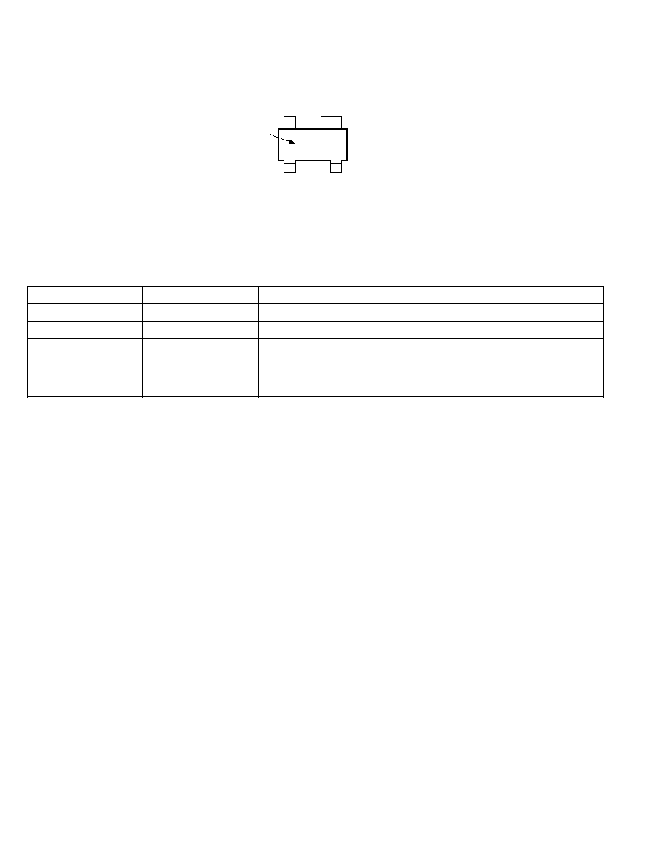
Pin Configuration
GND
CTL
G
VS
H10
Part
Identification
1
2
3
4
SOT-143 (M4)
Pin Description
Pin Number
Pin Name
Pin Function
1
GND
Ground: Power return.
2
VS
Supply (Input): +2.7V to +9V supply.
3
G
Gate (Output): Gate connection to external MOSFET.
4
CTL
Control (Input): TTL compatible on/off control input. Logic high drives the
gate output above the supply voltage. Logic low forces the gate output near
ground.
Early production identification:
MH10
1997
5-157
MIC5018
Micrel
5
Electrical Characteristics
Parameter
Condition (Note 1)
Min
Typ
Max
Units
Supply Current
V
SUPPLY
= 3.3V
V
CTL
= 0V
0.01
1
Á
A
V
CTL
= 3.3V
70
140
Á
A
V
SUPPLY
= 5V
V
CTL
= 0V
0
1
Á
A
V
CTL
= 5V
150
300
Á
A
Control Input Voltage
2.7V
V
SUPPLY
9V
V
CTL
for logic 0 input
0
0.8
V
2.7V
V
SUPPLY
5V
V
CTL
for logic 1 input
2.0
V
SUPPLY
V
5V
V
SUPPLY
9V
V
CTL
for logic 1 input
2.4
V
SUPPLY
V
Control Input Current
2.7V
V
SUPPLY
9V
0.01
1
Á
A
Control Input Capacitance
Note 2
5
pF
Zener Diode Output Clamp
V
SUPPLY
= 9V
13
16
19
V
Gate Output Voltage
V
SUPPLY
= 2.7V
6.3
7.1
V
V
SUPPLY
= 3.0V
7.1
8.2
V
V
SUPPLY
= 4.5V
11.4
13.4
V
Gate Output Current
V
SUPPLY
= 5V
V
OUT
= 10V, Note 3
9.5
Á
A
Gate Turn-On Time
V
SUPPLY
= 4.5V
C
L
= 1000pF, Note 4
0.75
1.5
ms
C
L
= 3000pF, Note 4
2.1
4.2
ms
Gate Turn-Off Time
V
SUPPLY
= 4.5V
C
L
= 1000pF, Note 5
10
20
Á
s
C
L
= 3000pF, Note 5
30
60
Á
s
General Note: Devices are ESD protected, however handling precautions are recommended.
Note 1:
Typical values at T
A
= 25
░
C. Minimum and maximum values indicate performance at ¡40
░
C
T
A
+85
░
C. Parts production tested at 25
░
C.
Note 2:
Guaranteed by design.
Note 3:
Resistive load selected for V
OUT
= 10V.
Note 4:
Turn-on time is the time required for gate voltage to rise to 4V greater than the supply voltage. This represents a typical MOSFET gate
threshold voltage.
Note 5:
Turn-off time is the time required for the gate voltage to fall to 4V above the supply voltage. This represents a typical MOSFET gate threshold
voltage.
Test Circuit
5V
0V
VS
CTL
G
GND
MIC5018
V
SUPPLY
1
2
3
4
C
L
V
OUT
0.1ÁF
Absolute Maximum Ratings
Supply Voltage (V
SUPPLY
) ........................................... +10V
Control Voltage (V
CTL
) ................................. ¡0.6V to +16V
Gate Voltage (V
G
) ....................................................... +16V
Ambient Temperature Range (T
A
) ............. ¡40
░
C to +85
░
C
Lead Temperature, Soldering 10sec. ........................ 300
░
C
Package Thermal Resistance
SOT-143
JA
..................................................... 220
░
C/W
SOT-143
JC
..................................................... 130
░
C/W
MIC5018
Micrel
5-158
1997
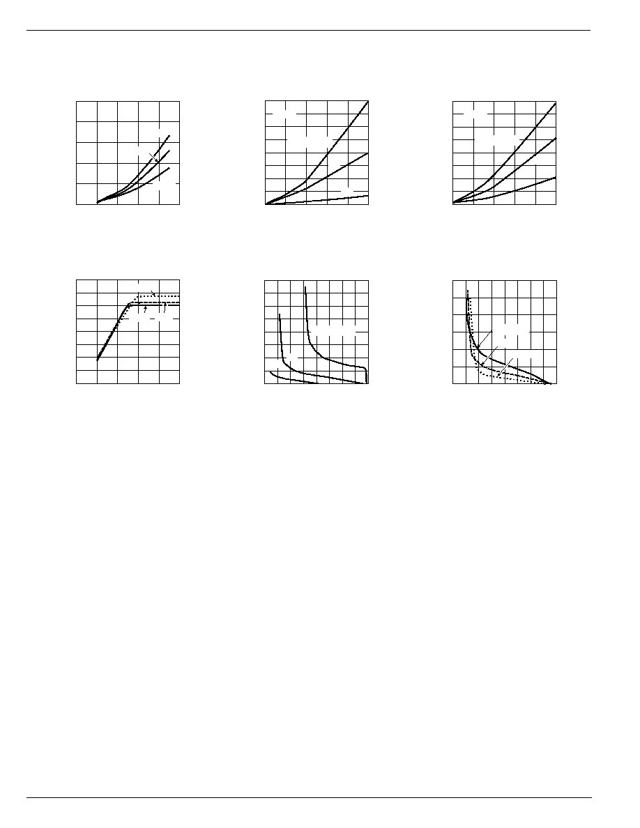
Typical Characteristics
Note 4
0
0.2
0.4
0.6
0.8
1.0
0
2
4
6
8
10
SUPPLY CURRENT (mA)
SUPPLY VOLTAGE (V)
Supply Current
vs. Supply Voltage
-40
░
C
125
░
C
25
░
C
0
40
80
120
160
0
2
4
6
8
10 12 14 16
OUTPUT CURRENT (
Á
A)
OUTPUT VOLTAGE (V)
Gate Output Current
vs. Output Voltage
V
SUPPLY
= 9V
5V
3V
0
1
2
3
4
5
6
7
8
0
1000 2000 3000 4000 5000
TURN-OFF TIME (
Á
s)
CAPACITANCE (pF)
Full Turn-Off Time
vs. Load Capacitance
V
SUPPLY
= 3V
5V
9V
Note 6
Note 4:
T
A
= 25
░
C, V
SUPPLY
= 5V unless noted.
Note 5:
Full turn-on time is the time between V
CTL
rising to 2.5V and the V
G
rising to 90% of its steady on-state value.
Note 6:
Full turn-off time is the time between V
CTL
falling to 0.5V and the V
G
falling to 10% of its steady on-state value.
0
5
10
15
20
0
1000 2000 3000 4000 5000
TURN-ON TIME (ms)
CAPACITANCE (pF)
Full Turn-On Time
vs. Load Capacitance
V
SUPPLY
= 3V
5V
9V
Note 5
0
5
10
15
20
0
2
4
6
8
10
OUTPUT VOLTAGE (V)
SUPPLY VOLTAGE (V)
Gate Output Voltage
vs. Supply Voltage
25
░
C
-40
░
C
125
░
C
0
20
40
60
80
100
120
0
2
4
6
8
10 12 14 16
OUTPUT CURRENT (
Á
A)
OUTPUT VOLTAGE (V)
Gate Output Current
vs. Output Voltage
T
A
= -55
░
C
25
░
C
125
░
C

1997
5-159
MIC5018
Micrel
5
Functional Description
Refer to the functional diagram.
The MIC5018 is a noninverting device. Applying a logic high
signal to CTL (control input) produces gate drive output. The
G (gate) output is used to turn on an external N-channel
MOSFET.
Supply
VS (supply) is rated for +2.7V to +9V. An external capacitor
is recommended to decouple noise.
Control
CTL (control) is a TTL compatible input. CTL must be forced
high or low by an external signal. A floating input may cause
unpredictable operation.
A high input turns on Q2, which sinks the output of current
source I1, making the input of the first inverter low. The
inverter output becomes high enabling the charge pump.
Charge Pump
The charge pump is enabled when CTL is logic high. The
charge pump consists of an oscillator and voltage quadrupler
Functional Diagram
CHARGE
PUMP
EN
VS
CTL
R2
15k
R1 2k
GND
G
MIC5018
+2.7V to +9V
Load
On
Off
I1
20ÁA
D1
16V
D2
35V
Q1
Q2
Q3
D3 16V
Functional Diagram with External Components
(High-Side Driver Configuration)
(4
Î
). Output voltage is limited to 16V by a zener diode. The
charge pump output voltage will be approximately:
V
G
= 4
Î
V
SUPPLY
¡ 2.8V, but not exceeding 16V.
The oscillator operates from approximately 70kHz to approxi-
mately 100kHz depending upon the supply voltage and
temperature.
Gate Output
The charge pump output is connected directly to the G (gate)
output. The charge pump is active only when CTL is high.
When CTL is low, Q3 is turned on by the second inverter and
discharges the gate of the external MOSFET to force it off.
If CTL is high, and the voltage applied to VS drops to zero, the
gate output will be floating (unpredictable).
ESD Protection
D1 and D2 clamp positive and negative ESD voltages. R1
isolates the gate of Q2 from sudden changes on the CTL
input. Q1 turns on if the emitter (CTL input) is forced below
ground to provide additional input protection. Zener D3 also
clamps ESD voltages for the gate (G) output.
MIC5018
Micrel
5-160
1997
Application Information
Supply Bypass
A capacitor from VS to GND is recommended to control
switching and supply transients. Load current and supply
lead length are some of the factors that affect capacitor
size requirements.
A 4.7
Á
F or 10
Á
F aluminum electrolytic or tantalum capacitor
is suitable for many applications.
The low ESR (equivalent series resistance) of tantalum
capacitors makes them especially effective, but also makes
them susceptible to uncontrolled inrush current from low
impedance voltage sources (such as NiCd batteries or auto-
matic test equipment). Avoid instantaneously applying volt-
age, capable of high peak current, directly to or near tantalum
capacitors without additional current limiting. Normal power
supply turn-on (slow rise time) or printed circuit trace resis-
tance is usually adequate for normal product usage.
MOSFET Selection
The MIC5018 is designed to drive N-channel enhancement-
type MOSFETs. The gate output (G) of the MIC5018 pro-
vides a voltage, referenced to ground, that is greater than the
supply voltage. Refer to the "Typical Characteristics: Gate
Output Voltage vs. Supply Voltage" graph.
The supply voltage and the MOSFET drain-to-source
voltage drop determine the gate-to-source voltage.
V
GS
= V
G
¡ (V
SUPPLY
¡ V
DS
)
where:
V
GS
= gate-to-source voltage (enhancement)
V
G
= gate voltage (from graph)
V
SUPPLY
= supply voltage
V
DS
= drain-to-source voltage (approx. 0V at
low current, or when fully enhanced)
VS
CTL
G
GND
MIC5018
V
SUPPLY
1
2
3
4
Load
V
GS
V
DS
V
LOAD
V
G
G
D
S
Figure 1. Voltages
The performance of the MOSFET is determined by the gate-
to-source voltage. Choose the type of MOSFET according to
the calculated gate-to-source voltage.
Standard MOSFET
Standard MOSFETs are fully enhanced with a gate-to-source
voltage of about 10V. Their absolute maximum gate-to-
source voltage is
▒
20V.
With a 5V supply, the MIC5018 produces a gate output of
approximately 15V. Figure 2 shows how the remaining
voltages conform. The actual drain-to-source voltage drop
across an IRFZ24 is less than 0.1V with a 1A load and 10V
enhancement. Higher current increases the drain-to-source
voltage drop, increasing the gate-to-source voltage.
VS
CTL
G
GND
MIC5018
4.7ÁF
+5V
1
2
3
4
Load
Logic
High
10V
approx. 0V
5V
15V
Voltages are approximate
* International Rectifier
standard MOSFET
IRFZ24*
To demonstrate
this circuit, try a
2
, 20W
load resistor .
Figure 2. Using a Standard MOSFET
The MIC5018 has an internal zener diode that limits the gate-
to-ground voltage to approximately 16V.
Lower supply voltages, such as 3.3V, produce lower gate
output voltages which will not fully enhance standard
MOSFETs. This significantly reduces the maximum current
that can be switched. Always refer to the MOSFET data sheet
to predict the MOSFET's performance in specific applica-
tions.
Logic-Level MOSFET
Logic-level N-channel MOSFETs are fully enhanced with a
gate-to-source voltage of approximately 5V and generally
have an absolute maximum gate-to-source voltage of
▒
10V.
VS
CTL
G
GND
MIC5018
4.7ÁF
+3.3V
1
2
3
4
Load
Logic
High
5.7V
approx. 0V
3.3V
9V
Voltages are approximate
* International Rectifier
logic-level MOSFET
IRLZ44*
To demonstrate
this circuit, try
5
, 5W or
47
, 1/4W
load resistors.
Figure 3. Using a Logic-Level MOSFET
Refer to figure 3 for an example showing nominal voltages.
The maximum gate-to-source voltage rating of a logic-level
MOSFET can be exceeded if a higher supply voltage is used.
An external zener diode can clamp the gate-to-source volt-
age as shown in figure 4. The zener voltage, plus its
tolerance, must not exceed the absolute maximum gate
voltage of the MOSFET.
VS
CTL
G
GND
MIC5018
V
SUPPLY
1
2
3
4
Load
5V < V
Z
< 10V
Protects gate of
logic-level MOSFET
Logic-level
N-channel
MOSFET
Figure 4. Gate-to-Source Protection
1997
5-161
MIC5018
Micrel
5
Split Power Supply
Refer to figure 6. The MIC5018 can be used to control a 12V
load by separating the driver supply from the load supply.
VS
CTL
G
GND
MIC5018
4.7ÁF
+12V
1
2
3
4
Load
Logic
High
3V
approx. 0V
12V
15V
Voltages are approximate
* International Rectifier
logic-level MOSFET
IRLZ44*
+5V
To demonstrate
this circuit, try a
40
, 5W or
100
, 2W
load resistor.
Figure 6. 12V High-Side Switch
A logic-level MOSFET is required. The MOSFET's maximum
current is limited slightly because the gate is not fully en-
hanced. To predict the MOSFETs performance for any pair
of supply voltages, calculate the gate-to-source voltage and
refer to the MOSFET data sheet.
V
GS
= V
G
¡ (V
LOAD SUPPLY
¡ V
DS
)
V
G
is determined from the driver supply voltage using the
"Typical Characteristics: Gate Output Voltage vs. Supply
Voltage" graph.
Low-Side Switch Configuration
The low-side configuration makes it possible to switch a
voltage much higher than the MIC5018's maximum supply
voltage.
On
Off
VS
CTL
G
GND
MIC5018
4.7ÁF
IRF540*
N-channel
MOSFET
+80V
1
2
3
4
Load
+2.7 to +9V
* International Rectifier
standard MOSFET
BV
DSS
= 100V
To demonstrate
this circuit, try
1k, 10W or
33k, 1/4W
load resistors.
Figure 7. Low-Side Switch Configuration
The maximum switched voltage is limited only by the
MOSFET's maximum drain-to-source ratings.
A gate-to-source zener may also be required when the
maximum gate-to-source voltage could be exceeded due to
normal part-to-part variation in gate output voltage. Other
conditions can momentarily increase the gate-to-source volt-
age, such as turning on a capacitive load or shorting a load.
Inductive Loads
Inductive loads include relays, and solenoids. Long leads
may also have enough inductance to cause adverse effects
in some circuits.
On
Off
VS
CTL
G
GND
MIC5018
4.7ÁF
+2.7V to +9V
1
2
3
4
Schottky
Diode
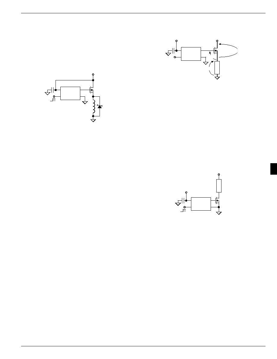
Figure 5. Switching an Inductive Load
Switching off an inductive load in a high-side application
momentarily forces the MOSFET source negative (as the
inductor opposes changes to current). This voltage spike can
be very large and can exceed a MOSFET's gate-to-source
and drain-to-source ratings. A Schottky diode across the
inductive load provides a discharge current path to minimize
the voltage spike. The peak current rating of the diode should
be greater than the load current.
In a low-side application, switching off an inductive load will
momentarily force the MOSFET drain higher than the supply
voltage. The same precaution applies.