March 2005
1
M9999-031805
MIC2550A
Micrel, Inc.
Ordering Information
Part Number
Standard
Pb-Free
Package
MIC2550ABTS
MIC2550AYTS
14-Pin TSSOP
MIC2550ABML
MIC2550AYML
16-Pin MLFTM
MIC2550A
Universal Serial Bus Transceiver
General Description
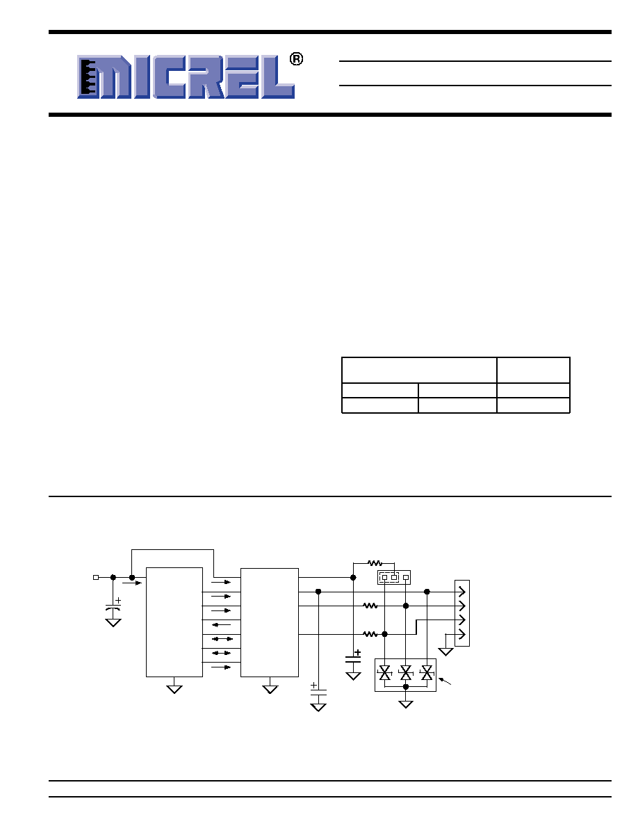
The MIC2550A is a single-chip transceiver that complies with
the physical layer specifications for Universal Serial Bus
(USB).
The MIC2550A supports full-speed (12Mbps) and low-speed
(1.5Mbps) operation and introduces superior edge rate con-
trol to produce crisper eye diagrams. As a result, the task of
passing USB compliance testing is made easier.
A unique, patented, dual supply voltage operation allows the
MIC2550A to reference the system I/F I/O signals to a supply
voltage down to 2.5V while independently powered by the
USB V
BUS
. This allows the system interface to operate at its
core voltage without addition of buffering logic and also
reduce system operating current.
System Diagram
Features
· Compliant to USB Specification Revision 2.0 for
low-speed (1.5Mbps) and full-speed (12Mbps) operation
· Compliant to IEC-61000-4.2 (Level 2)
· Operation down to 2.5V
· Dual supply voltage operation
· Integrated speed-select termination supply
· Very low power consumption meets USB suspend-
current requirements
· Small 14-pin TSSOP and 16-pin MLFTM packages
Applications
· Personal digital assistants (PDA)
· Palmtop computers
· Cellular telephones
System
Supply Voltage
System
Interface
VIF
SPD
OE#
RCV
VP
D
VM
D
D+
VBUS
VTRM
GND
D
D+
V
BUS
USB
Interface
Connector
Cooper Electronics Technologies
41206ESDA SurgX
GND
R
S
24
R
S
24
1.5k
GND
HIGH
SPEED
LOW
SPEED
MIC2550A
SUS
1µF
1µF min
10µF max
0.47µF
(See "Applications Information"
for additional suppliers.)
Micrel, Inc. · 2180 Fortune Drive · San Jose, CA 95131 · USA · tel + 1 (408) 944-0800 · fax + 1 (408) 474-1000 · http://www.micrel.com
MicroLeadFrame and MLF are trademarks of Amkor Technology.
SurgX is a registered trademark of Cooper Electronics Technologies.

MIC2550A
Micrel, Inc.
M9999-031805
2
March 2005
Pin Description
Pin Name
Pin Number
Pin Number
Pin Function
MIC2550ABTS
MIC2550ABML
VIF
1
15
System Interface Supply Voltage (Input): Determines logic voltage levels for
system interface signaling to logic controller.
SPD
2
1
Speed (Input): Edge rate control. Logic high selects full-speed edge rates.
Logic low selects low-speed edge rates.
RCV
3
2
Receive Data (Output): System interface receive data interface to logic
controller.
VP
4
3
Plus (Input/Output): System interface signal to logic controller. If OE# is
logic 1, VP is a receiver output (+); If OE# is logic 0, VP is a driver input (+).
VM
5
4
Minus (Input/Output): System interface signal to logic controller. If OE# is
logic 1, VM is a receiver output (); If OE# is logic 0, VM is a driver input ().
NC
6, 13
5, 8, 13 16
Not internally connected
GND
7
6
Ground: Power supply return and signal reference.
SUS
8
7
Suspend (Input): Logic high turns off internal circuits to reduce supply
current.
OE#
9
9
Output Enable (Input): Active low system interface input signal from logic
controller. Logic low causes transceiver to transmit data onto the bus. Logic
high causes the transceiver to receive data from the bus.
D
10
10
USB Differential Data Line (Input/Output)
D+
11
11
USB Differential Data Line + (Input/Output)
VTRM
12
12
Termination Supply (Output): 3.3V speed termination resistor supply output.
VBUS
14
14
USB Supply Voltage (Input): Transceiver supply.
Pin Configuration
1
VIF
SPD
RCV
VP
VM
NC
GND
14 VBUS
NC
VTRM
D+
D
OE#
SUS
13
12
11
10
9
8
2
3
4
5
6
7
14-Pin TSSOP (TM)
1
2
3
4
12
11
10
9
16 15 14 13
5
6
7
8
SPD
RCV
VP
VM
VTRM
D+
D
OE#
NC
VBUS
VIF
NC
NC
SUS
GND
NC
16-Pin MLFTM (ML)
March 2005
3
M9999-031805
MIC2550A
Micrel, Inc.
Absolute Maximum Ratings
(Note 1)
Supply Voltage (V
IF
) ................................................... +6.5V
Input Voltage (V
BUS
) ........................ 0.5V(min)/5.5V(max)
Output Current (I
D+
, I
D
) ........................................... ±50mA
Output Current (all others) ....................................... ±15mA
Input Current ............................................................ ±50mA
Storage Temperature (T
S
) ......................... 65° to +150°C
ESD, Note 3
V
BUS
, D+, D ......................................................... ±10kV
All other pins ........................................................... ±2kV
Operating Ratings
(Note 2)
Supply Voltage (V
BUS
) ................................. 4.0V to 5.25V
Temperature Range (T
A
) ........................... 40°C to +85°C
Junction Temperature (T
J
) ........................................ 160°C
Package Thermal Resistance
TSSOP (
JA
) ..................................................... 100°C/W
Electrical Characteristics
(Note 8)
T
A
= 25°C, bold values indicate 40°C T
A
+85°C; typical values at V
BUS
= 5.0V, V
IF
= 3.0V; minimum and maximum values at
V
BUS
= 4.0V to 5.25V, V
IF
= 2.5V to 3.6V; unless noted.
Symbol
Parameter
Condition
Min
Typ
Max
Units
System and USB Interface DC Characteristics
V
BUS
USB Supply Voltage
4.0
5.25
V
V
IF
System I/F Supply Voltage
2.5
5.25
V
V
IL
Low-Level Input Voltage, Note 4
0.15V
IF
V
V
IH
High-Level Input Voltage, Note 4
0.85V
IF
V
V
OH
High-Level Output Voltage, Note 4
I
OH
= 20µA
0.9V
IF
V
V
OL
Low-Level Output Voltage, Note 4
I
OL
= 20µA
0.1
V
I
IL
Input Leakage Current, Note 4
±5
µA
Symbol
Parameter
Conditions
Min
Typ
Max
Units
SPD
SUS
OE#
Voltage
Load
1
0
1
1
5
µA
1
0
0
1
5
µA
0
0
1
1
5
µA
I
IF
VIF Supply Current
0
0
0
VBUS = 5.25V
1
5
µA
0
1
0
VIF = 3.6V
1
5
µA
1
0
0
f = 6MHz CLOAD
325
650
µA
= 50 pF, Note 7
f = 750kHz
0
0
0
CLOAD = 600 pF
40
75
µA
Note 7
1
0
1
800
1100
µA
1
0
0
3000
5000
µA
0
0
1
230
350
µA
0
0
0
400
700
µA
I
VBUS
VBUS Supply Current
0
1
0
VBUS = 5.25V
130
200
µA
1
0
0
VIF = 3.6V
f = 6MHz CLOAD
7.3
10
mA
= 50 pF, Note 7
f = 750kHz
0
0
0
CLOAD = 600 pF
3.6
5
mA
Note 7
V
TRM
Termination Voltage
I
TRM
= 2.5mA
3.0
3.6
V
ESD Protection
IEC-1000-4-2
Air Discharge
10 pulses
±6
kV
(D+, D,
Contact Discharge
10 pulses
±6
kV
V
BUS
only)
MIC2550A
Micrel, Inc.
M9999-031805
4
March 2005
Symbol
Parameter
Condition
Min
Typ
Max
Units
Transceiver DC Characteristics
I
LO
Hi-Z State Data Line Leakage
0V < V
BUS
< 3.3V, D+, D, OE# = 1 pins only
10
+10
µA
V
DI
Differential Input Sensitivity
|(D+) (D)|, V
IN
= 0.8V 2.5V
0.2
V
V
CM
Differential Common-Mode Range
Includes V
DI
range
0.8
2.5
V
V
SE
Single-Ended Receiver Threshold
0.8
2.0
V
Receiver Hysteresis, Note 6
200
mV
V
OL
Static Output Low, Note 5
OE# = 0, R
L
= 1.5k to 3.6V
0.3
V
V
OH
Static Output High, Note 5
OE# = 0, R
L
= 15k to GND
2.8
3.6
V
V
CRS
Output Signal Crossover Voltage
1.3
2.0
V
Note 6
C
IN
Transceiver Capacitance, Note 6
Pin to GND
20
pF
Z
DRV
Driver Output Resistance
Steady state drive, Note 6
6
18
Low-Speed Driver Characteristics, Note 7
t
R
Transition Rise Time
C
L
= 50pF
75
ns
C
L
= 600pF
300
ns
t
F
Transition Fall Time
C
L
= 50pF
75
ns
C
L
= 600pF
300
ns
t
R
/t
F
Rise and Fall Time Matching
T
R
÷ T
F
80
125
%
V
CRS
Output Signal Crossover Voltage
1.3
2.0
V
Full-Speed Driver Characteristics, Note 7
t
R
Transition Rise Time
C
L
= 50pF
4
20
ns
t
F
Transition Fall Time
C
L
= 50pF
4
20
ns
t
R
/t
F
Rise and Fall Time Matching
T
R
÷ T
F
90
111.11
%
V
CRS
Output Signal Crossover Voltage
1.3
2.0
V
Transceiver Timing, Note 7
t
PVZ
OE# to RCVR Tri-state Delay
Figure 1
15
ns
t
PZD
Receiver Tri-state to Transmit Delay
Figure 1
15
ns
t
PDZ
OE# to DRVR Tri-state Delay
Figure 1
15
ns
t
PZV
Driver Tri-state to Receiver Delay
Figure 1
15
ns
t
PLH
V+/V to D+/D Propagation Delay
Figure 4
15
ns
t
PHL
V+/V to D+/D Propagation Delay
Figure 4
15
ns
t
PLH
D+/D to RCV Propagation Delay
Figure 3
15
ns
t
PHL
D+/D to RCV Propagation Delay
Figure 3
15
ns
t
PLH
D+/D to V+/D Propagation Delay
Figure 3
8
ns
t
PHL
D+/D to V+/D Propagation Delay
Figure 3
8
ns
Note 1.
Exceeding the absolute maximum rating may damage the device.
Note 2.
The device is not guaranteed to function outside its operating rating.
Note 3.
Devices are ESD sensitive. Handling precautions recommended. Human body model, 1.5k in series with 100pF.
Note 4.
Applies to the VP, VM, RCV, OE#, SPD, and SUS pins.
Note 5.
Applies to D+, D.
Note 6.
Not production tested. Guaranteed by design.
Note 7.
Characterized specification(s), but not production tested.

March 2005
5
M9999-031805
MIC2550A
Micrel, Inc.
V
M
V
P
V
P
/V
M
t
PVZ
t
PZV
V
OE#
H
L
t
PZD
V
D+
/V
D
V
D
V
D+
Figure 1. Enable and Disable Times
10%
V
D
V
D+
Differential
Data
Lines
90%
t
R
t
F
V
CRS
Figure 2. Rise and Fall Times
V
D
V
D+
Differential
Data
Lines
t
PLH
t
PHL
Output
V
OH
V
OL
V
SS
Figure 3. Receiver Propagation Delay D+/D to RCV, V
P
, and V
M
V
D
V
D+
Differential
Data
Lines
t
PLH
t
PHL
Input
V
OI
V
OL
V
SS
Figure 4. Driver Propagation Delay V
P
and V
M
to D+/D
Timing Diagrams
MIC2550A
Micrel, Inc.
M9999-031805
6
March 2005
:
)
t
i
m
s
n
a
r
T
(
0
=
#
E
O
t
u
p
n
I
t
u
p
t
u
O
t
l
u
s
e
R
P
V
M
V
+
D
D
V
C
R
0
0
0
0
X
0
E
S
0
1
0
1
0
0
c
i
g
o
L
1
0
1
0
1
1
c
i
g
o
L
1
1
1
1
X
d
e
n
i
f
e
d
n
U
:
)
e
v
i
e
c
e
R
(
1
=
#
E
O
t
u
p
n
I
t
u
p
t
u
O
t
l
u
s
e
R
+
D
D
P
V
M
V
V
C
R
0
0
0
0
X
0
E
S
0
1
0
1
0
0
c
i
g
o
L
1
0
1
0
1
1
c
i
g
o
L
1
1
1
1
X
d
e
n
i
f
e
d
n
U
Note. X = undefined.
Table 1. Truth Table
Test Circuits
Device
Under
Test
50pF
24
For D+, D:
V = 0V for t
PZH
and t
PHZ
V = V
BUS
for t
PZL
and t
PLZ
V
Test
Point
500
Figure 5. Load for Enable and Disable Time (D+, D)
Device
Under
Test
25pF
Figure 6. V
P
, V
M
and RCV Load
Device
Under
Test
15k
C
L
V
TRM
1.5k*
24
C
L
= 50pF, full speed
C
L
= 50pF, low speed (minimum timing)
C
L
= 600pF, low speed (maximum timing)
*1.5k on D for low speed or D+ for high speed
Figure 7. D+ and D Load
March 2005
7
M9999-031805
MIC2550A
Micrel, Inc.
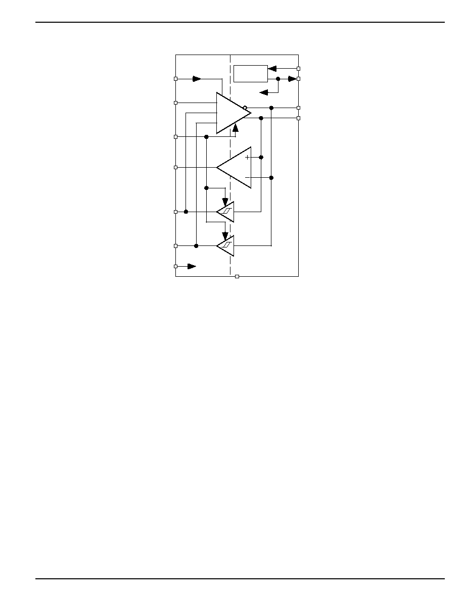
Block Diagram
Regulator
VM
GND
VP
RCV
OE#
SPD
VIF
D
D+
VBUS
VTRM
USB VOLTAGE DOMAIN
SYSTEM I/F
VOLTAGE DOMAIN
TO
INTERNAL
CIRCUITS
SUS
MIC2550A
Micrel, Inc.
M9999-031805
8
March 2005
Applications Information
The MIC2550A is designed to provide USB connectivity in
mobile systems where system supply voltages are not avail-
able to satisfy USB requirements. The MIC2550A can oper-
ate down to supply voltages of 2.5V and still meet USB
physical layer specifications. As shown in the system dia-
gram, the MIC2550A takes advantage of USB's supply
voltage, V
BUS
, to operate the transceiver. The system volt-
age, V
IF
, is used to set the reference voltage used by the
digital I/O lines (VP, VM, RCV, OE#, SPD, and SUS pins)
interfacing to the system. Internal circuitry provides transla-
tion between the USB and system voltage domains. V
IF
will
typically be the main supply voltage rail for the system.
In addition, a 3.3V, 10% termination supply voltage, V
TRM
, is
provided to support speed selection. A 0.47µF (minimum)
capacitor from V
TRM
to ground is required to ensure stability.
A 1.5K resistor is required between this pin and the D+ or D
lines to respectively specify full-speed or low-speed opera-
tion.
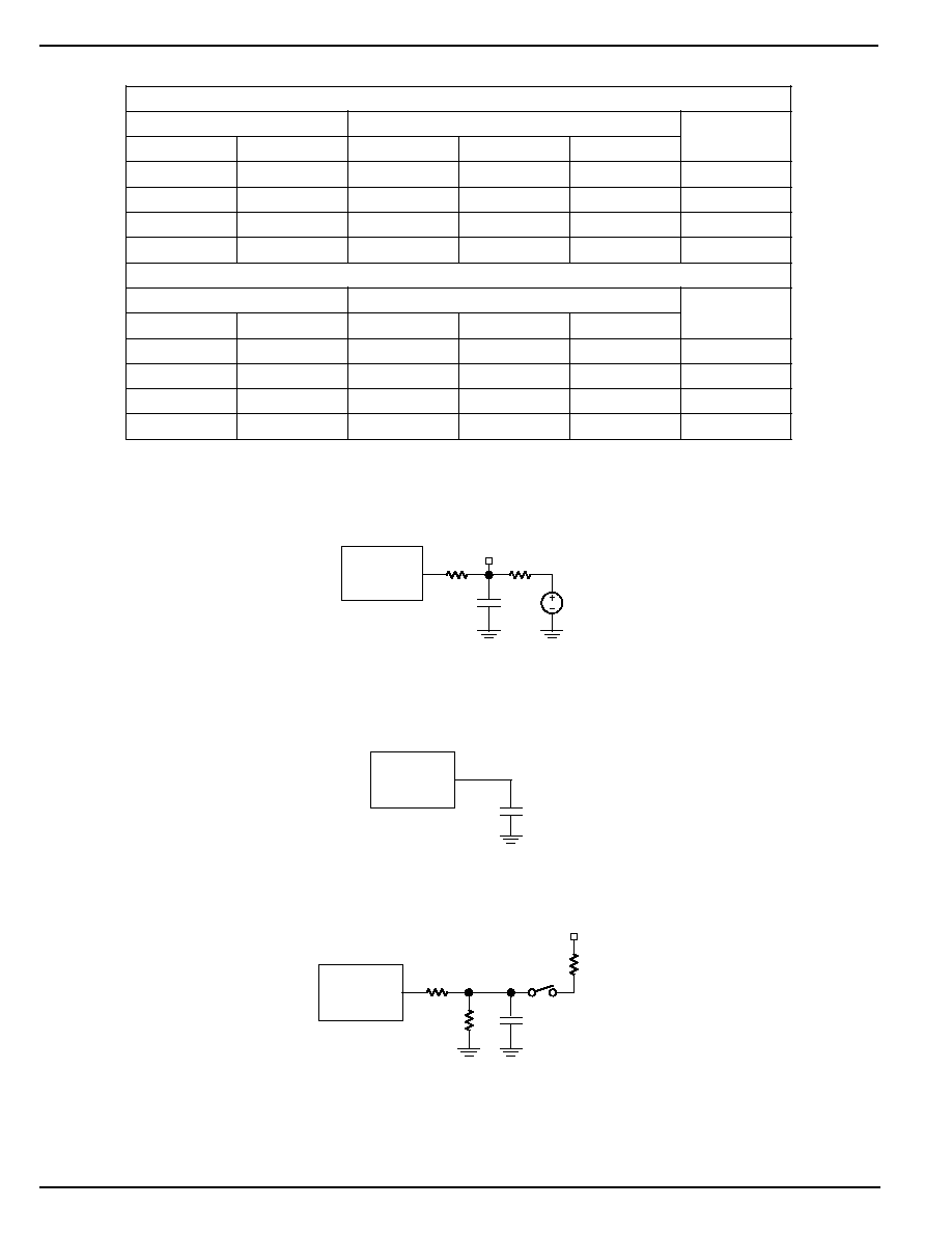
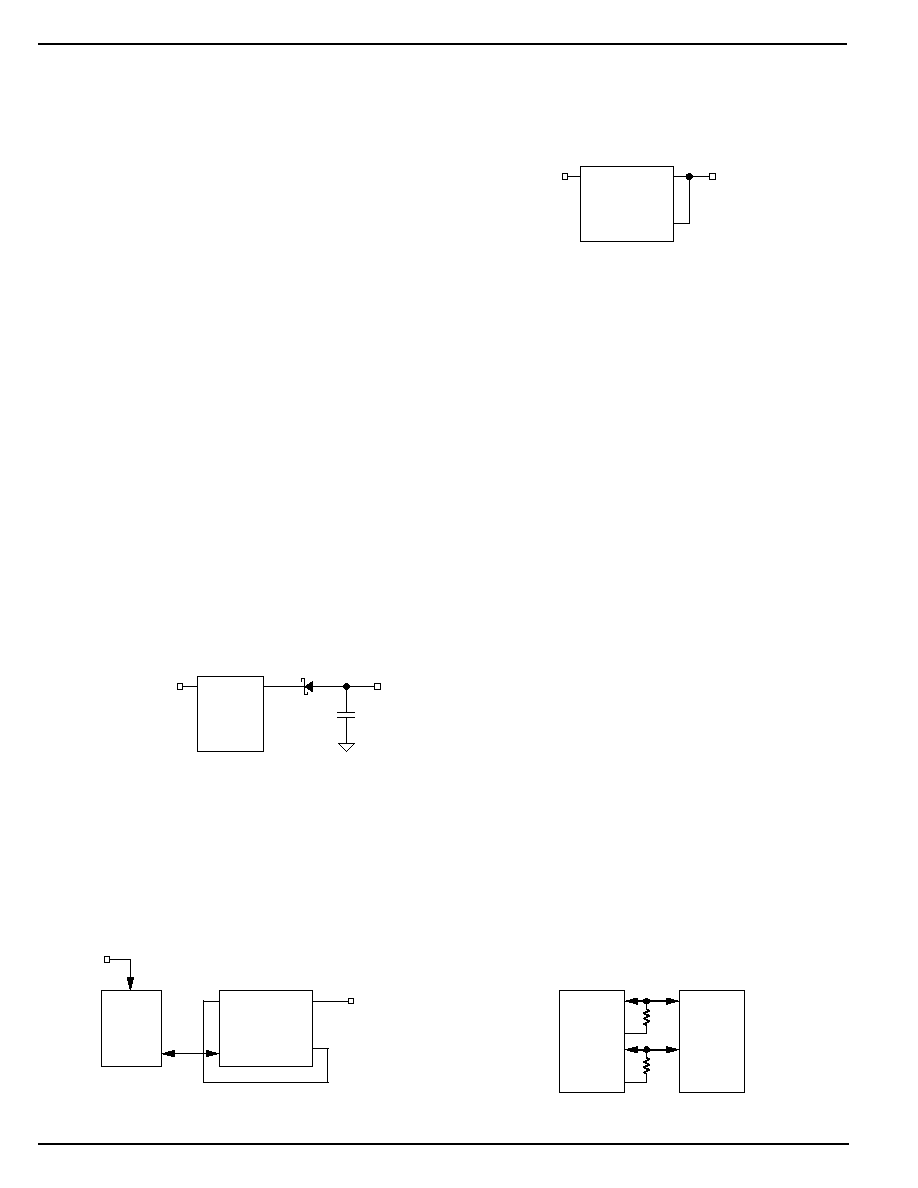
Power Supply Configurations
V
IF
/V
BUS
Switched
When the V
BUS
input pin is pulled to ground a low impedance
path between V
IF
and V
BUS
can cause a high current flow
from V
IF
to V
BUS
thereby damaging the MIC2550A. This
issue can arise in systems where V
BUS
is driven from a power
supply that can be switched off such as in the case of a
desktop PC. Adding a Schottky diode, such as the ZHCS1000
by Zetex, in series with V
BUS
will prevent any current flow
during this condition. A solution is shown in Figure 8 below.
If the V
IF
source is current limited to less than 50mA, then
diode D1 is not necessary.
MIC2550
VIF
Note: *(Optional) See Text - Power Supply Configurations
VBUS
1µF min
VBUS
USB Device
Power Controller
*(Optional)
D1
ZHCS1000 or
equivalent
Figure 8. Solution to V
IF
/V
BUS
Switching
I/O Interface Using 3.3V
In systems where the I/O interface utilizes a 3.3V USB
controller, an alternate solution is shown in Figure 9. This
configuration has the advantage over Figure 8, in that no
extra components are needed. Ensure that the load on V
TRM
does not exceed 1mA total.
MIC2550
VIF
VBUS
I/O
VBUS
V
P
/V
M
/
RCV/OE#
VTRM
USB
Controller
V
DD
3.3V
Figure 9. I/O Interface Using 3.3V
Internal 3.3V Source
If the device is self-powered and has 3.3V available, the
circuit in Figure 10 is yet another power supply configuration
option. In this configuration, the internal regulator is disabled
and the 3.3V source and not V
BUS
powers the entire chip.
MIC2550A
VIF
3.3V
VBUS
VTRM
Figure 10. Powering Chip
from Internal 3.3V Source
Suspend
When the suspend pin (SUS) is high, power consumption is
reduced to a minimum. V
TRM
is not disabled. RCV, V
P
and V
M
are still functional to enable the device to detect USB activity.
For minimal current consumption in suspend mode, it is
recommended that OE# = 1, and SPD = 0.
Speed
The speed pin (SPD) sets D+/D output edge rates by increas-
ing or decreasing biasing current sources within the output
drivers. For low speed, SPD = 0. For full speed, SPD = 1. By
setting SPD = 0 during idle periods, in conjunction with suspend
(SUS), the lowest quiescent current can be obtained. However,
designers must provide a 300ns delay between changing SPD
from 0 to 1 and transmission of data at full speed. This delay
ensures the output drivers have arrived at their proper operating
conditions. Failure to do so can result in leading edge distortion
on the first few data bits transmitted.
External ESD Protection
The use of ESD transient protection devices is not required
for operation, but is recommended. We recommend the
following devices or the equivalent:
Cooper Electronics Technologies (www.cooperet.com)
41206ESDA SurgX
®
0805ESDA SurgX
®
Littelfuse (www.littlefuse.com)
V0402MHS05
SP0503BAHT
Non-multiplexed Bus
To save pin count for the USB logic controller interface, the
MIC2550A was designed with V
P
and V
M
as bidirectional
pins. To interface the MIC2550A with a non-multiplexed data
bus, resistors can be used for low cost isolation as shown in
Figure 11.
V
PO
V
P
V
M
V
MO
USB Logic
Controller
(SIE)
MIC2550
V
P
V
M
10k
10k
Figure 11. MIC2550A Interface to
Non-multiplexed Data Bus

March 2005
9
M9999-031805
MIC2550A
Micrel, Inc.
PCB Layout Recommendations
Although the USB standard and applications are not based in
an impedance controlled environment, a properly designed
PCB layout is recommended for optimal transceiver perfor-
mance. The suggested PCB layout hints are as follows:
· Match signal line traces (VP/VM, D+, D) to
40ps, approximately
1
/
3
inch if possible. FR-4
PCB material propagation is about 150ps/inch,
so to minimize skew try to keep VP/VM, D+/D
traces as short as possible.
· For every signal line trace width (w), separate
the signal lines by 1.52 widths. Place all other
traces at >2w from all signal line traces.
· Maintain the same number of vias on each
differential trace, keeping traces approximately
at same separation distance along the line.
· Control signal line impedances to ±10%.
· Keep R
S
as close to the IC as possible, with
equal distance between R
S
and the IC for both
D+ and D.

MIC2550A
Micrel, Inc.
M9999-031805
10
March 2005
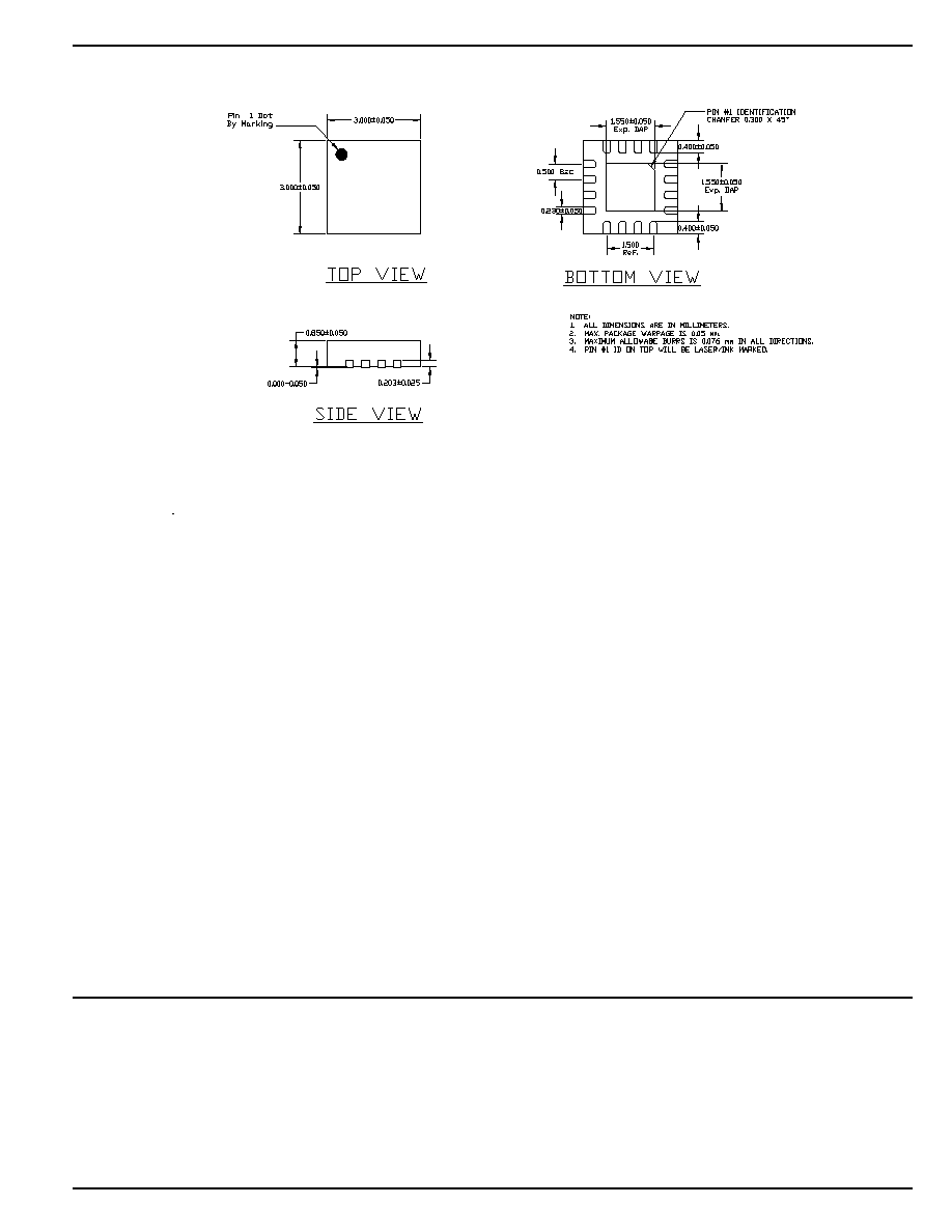
Package Information
1.10 MAX (0.043)
0.15 (0.006)
0.05 (0.002)
1.00 (0.039) REF
0.65 BSC
(0.026)
8°
0°
6.4 BSC (0.252)
5.10 (0.200)
4.90 (0.193)
0.20 (0.008)
0.09 (0.003)
0.70 (0.028)
0.50 (0.020)
DIMENSIONS:
MM (INCH)
4.50 (0.177)
4.30 (0.169)
0.30 (0.012)
0.19 (0.007)
14-Pin TSSOP (TS)
3.00BSC
2.75BSC
0.50 DIA
3.00BSC
12° max
SEATING
PLANE
2.75BSC
16
1
1
2
3
4
N
2
3
4
0.85
+0.15
0.65
0.65
+0.15
0.65
0.01
+0.04
0.01
0.23
+0.07
0.05
0.01
+0.04
0.01
0.42
+0.18
0.18
0.42
+0.18
0.18
0.23
+0.07
0.05
1.60
+0.10
0.10
PIN 1 ID
0.5 BSC
1.5 REF
0.42
+0.18
0.18
1.60
+0.10
0.10
0.40
+0.05
0.05
0.20 REF.
0.5BSC
SECTION "C-C"
SCALE: NONE
TOP VIEW
BOTTOM VIEW
1. DIMENSIONS ARE IN mm.
2. DIE THICKNESS ALLOWABLE IS 0.305mm MAX.
3. PACKAGE WARPAGE MAX 0.05mm.
4. THIS DIMENSION APPLIES TO PLATED TERMINAL AND IS MEASURED
BETWEEN 0.20mm AND 0.25mm FROM TIP.
5. APPLIES ONLY FOR TERMINALS
C C
CL
4
Rev. 02
16-Pin MLFTM (ML)
March 2005
11
M9999-031805
MIC2550A
Micrel, Inc.
MICREL INC.
2180 FORTUNE DRIVE
SAN JOSE, CA 95131
USA
TEL
+ 1 (408) 944-0800
FAX
+ 1 (408) 474-1000
WEB
http://www.micrel.com
This information furnished by Micrel in this data sheet is believed to be accurate and reliable. However no responsibility is assumed by Micrel for its use.
Micrel reserves the right to change circuitry and specifications at any time without notification to the customer.
Micrel Products are not designed or authorized for use as components in life support appliances, devices or systems where malfunction of a product can
reasonably be expected to result in personal injury. Life support devices or systems are devices or systems that (a) are intended for surgical implant into
the body or (b) support or sustain life, and whose failure to perform can be reasonably expected to result in a significant injury to the user. A Purchaser's
use or sale of Micrel Products for use in life support appliances, devices or systems is a Purchaser's own risk and Purchaser agrees to fully indemnify
Micrel for any damages resulting from such use or sale.
© 2003 Micrel, Incorporated.
16-Pin MLFTM (ML)