
MIC2514
Micrel
6-18
1997
MIC2514
IttyBittyTM Integrated High-Side Switch
Preliminary Information
General Description
The MIC2514 is an integrated high-side power switch that
consists of a TTL compatible input and protected
P-channel MOSFET. The MIC2514 can be used instead of
a separate high-side driver and MOSFET in many low-
voltage applications.
The MIC2514 switches voltage ranging from 3V to 13.5V and
delivers more than 400mA continuous current. A slow turn-
on feature prevents high inrush current when switching
capacitive loads. The internal control circuitry is powered
from the unswitched 3V to 13.5V input.
Current limiting is internally fixed at approximately 1.9A and
requires no external components.
Thermal shutdown turns off the output if the die temperature
exceeds approximately 170
°
C.
The MIC2514 is available in the 5-lead SOT-23-5 package
with a temperature range of 40
°
C to +85
°
C.
Pin Configuration
Typical Application
Features
· MOSFET on-resistance
1.5
typical at 5V
0.95
typical at 12V
· 3V to 13.5V input
· 25
µ
A typical on-state supply current at 5V
· <1
µ
A typical off-state supply current at 5V
· Current limit
· Thermal shutdown
· Slow turn-on
Applications
· 3.3V to 13.5V power management
Ordering Information
Part Number
Temperature Range
Package
MIC2514BM5
40
°
C to +85
°
C
SOT-23-5
Part
Identification
CTL
NC
OUT
IN
F10
1
3
4
5
2
GND
5-Lead SOT-23-5 (M5)
On
Off
IN
OUT
MIC2514
1
3
GND
4
CTL
2
0.1µF
3V to 13.5V
Load
High-Side Power Switch
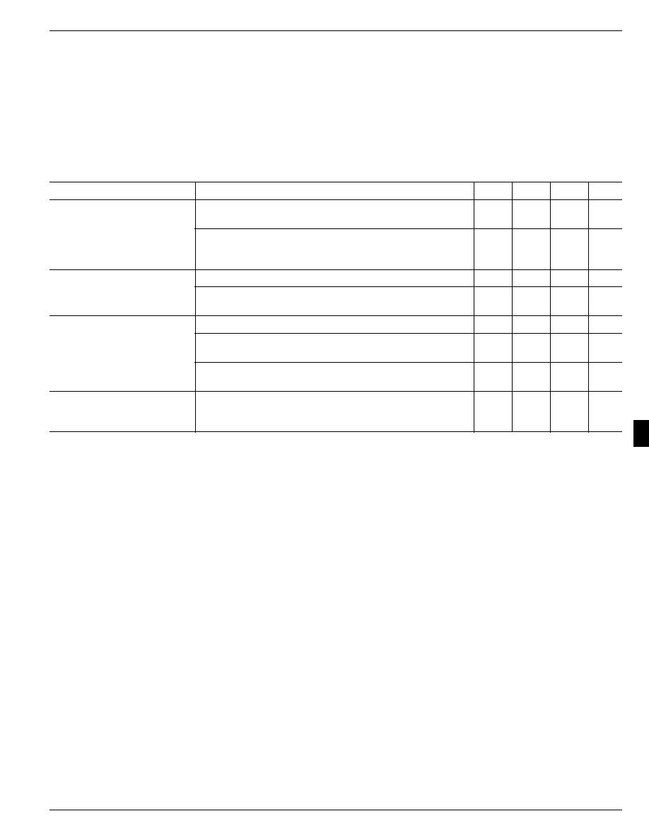
Pin Description
Pin Number
Pin Name
Pin Function
1
CTL
Control (Input): Noninverting TTL compatible control input.
High = on, low = off.
2
GND
Ground
3
IN
Supply Input: Output MOSFET source. Also supplies IC's internal circuitry.
Connect to supply.
4
OUT
Switch Output: Output MOSFET drain. Connect to switched side
of load.
5
NC
Not internally connected. Connect to ground plane for lowest package
thermal resistance.
1997
6-19
MIC2514
Micrel
6
Absolute Maximum Ratings
Supply Voltage (V
IN
) ................................................... +20V
Output Current (I
OUT
) ............................... Internally Limited
Control Input (V
CTL
) ....................................... 0.3V to 15V
Storage Temperature (T
A
) ....................... 65
°
C to +150
°
C
Operating Ratings
Supply Voltage (V
IN
) .................................... +3V to +13.5V
Ambient Operating Temperature (T
A
) ........ 40
°
C to +85
°
C
Thermal Resistance
(
JA
) ................................................................... 220
°
C/W
(
JC
) .................................................................. 130
°
C/W
Electrical Characteristics
V
IN
= +5V; T
A
= 25
°
C, except bold values indicate 40
°
C
T
A
85
°
C, Note 1; unless noted.
Parameter
Condition
Min
Typ
Max
Units
Supply Current
V
CTL
= logic 0, V
IN
= 5V
0.6
10
µ
A
V
CTL
= logic 0, V
IN
= 13.5V
2.0
25
µ
A
V
CTL
= logic 1, V
IN
= 3V
10
20
µ
A
V
CTL
= logic 1, V
IN
= 5V
25
40
µ
A
V
CTL
= logic 1, V
IN
= 13.5V
95
200
µ
A
Control Input Voltage
V
CTL
= logic 0, 3V
V
IN
13.5V
0
0.8
V
V
CTL
= logic 1, 3V
V
IN
5V
0.8
1.45
2.0
V
V
CTL
= logic 1, 5V
V
IN
13.5V
0.8
1.65
2.3
V
Output MOSFET Resistance
V
IN
= 3V
2.4
4.5
V
IN
= 5V
1.5
2.4
2.7
V
IN
= 12V
.95
1.5
1.7
Current Limit Threshold
V
IN
= 3V
0.5
1.5
A
V
IN
= 5V
1.0
1.4
2.0
A
V
IN
= 12V
1.2
1.9
2.5
A
General Note: Devices are ESD protected, however, handling precautions recommended.
Note 1: Devices production tested at 25
°
C, but Devices guaranteed over indicated temperature range.
MIC2514
Micrel
6-20
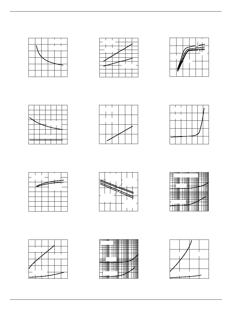
1997
0
0.5
1.0
1.5
2.0
0
5
10
15
CONTROL VOLTAGE (V)
SUPPLY VOLTAGE (V)
Control Input Threshold
vs. Supply Voltage
T
A
= 25
°
C
CTL
RISING
CTL
FALLING
0
0.5
1.0
1.5
2.0
2.5
-60 -30
0
30
60
90 120 150
THRESHOLD (V)
TEMPERATURE (
°
C)
Control Input Threshold
vs. Temperature
V
CTL
=
a
V
IN
= 5V
V
CTL
=
_
V
IN
= 5V
V
CTL
=
_
V
S
= 13.5V
V
CTL
=
a
V
S
= 13.5V
1
10
100
0.1
1
10
100
1000
TURN-ON DELAY TIME (
µ
s)
LOAD CAPACITANCE (nF)
Turn-On Delay Time
vs. Load Capacitance
I
L
= 5mA, T
A
= 25
°
C
V
IN
= 13.5V
V
IN
= 5V
0
20
40
60
0
0.2
0.4
0.6
0.8
1.0
1.2
TURN-ON DELAY TIME (
µ
s)
LOAD CURRENT (A)
Turn-On Delay Time
vs. Load Current
V
IN
= 5V
V
IN
= 13.5V
T
A
= 25
°
C
1
10
100
0.1
1
10
100
1000
RISE TIME (
µ
s)
LOAD CAPACITANCE (nF)
Rise Time
vs. Load Capacitance
V
IN
= 5V
V
IN
= 13.5V
T
A
= 25
°
C
0
20
40
60
80
0
0.4
0.8
1.2
1.6
RISE TIME (
µ
s)
LOAD CURRENT (A)
Rise Time
vs. Load Current
V
IN
= 13.5V
V
IN
= 5V
T
A
= 25
°
C
Typical Characteristics
0
1
2
3
0
5
10
15
ON-RESISTANCE (
)
SUPPLY VOLTAGE (V)
On-Resistance
vs. Supply Voltage
V
CTL
= 5V
T
A
= 25
°
C
0
0.5
1.0
1.5
2.0
2.5
-80
-40
0
40
80
120 160
ON-RESISTANCE (
)
AMBIENT TEMPERATURE (
°
C)
On-Resistance
vs. Temperature
V
CTL
= 5V
V
IN
= 5V
V
IN
= 13.5V
0
0.5
1.0
1.5
2.0
2.5
0
5
10
15
CURRENT LIMIT (A)
SUPPLY VOLTAGE (V)
Current Limit
vs. Supply Voltage
-25
°
C
25
°
C
75
°
C
125
°
C
0
50
100
150
200
-60 -30
0
30
60
90 120 150
SUPPLY CURRENT (
µ
A)
TEMPERATURE (
°
C)
On-State Supply Current
vs. Temperature
V
IN
= 13.5V
V
IN
= 5V
0
0.5
1.0
1.5
2.0
2.5
-60 -30
0
30
60
90 120 150
SUPPLY CURRENT (
µ
A)
TEMPERATURE (
°
C)
Off-State Supply Current
vs. Temperature
V
IN
= 5V
V
CTL
= 0V
0
1
2
3
4
0
5
10
15
SUPPLY CURRENT (
µ
A)
SUPPLY VOLTAGE (V)
Off-State Current Supply
vs. Supply Voltage
T
A
= 25
°
C
V
CTL
= 0V

1997
6-21
MIC2514
Micrel
6
Typical Characteristics
0.01
0.1
1
10
0.1
1
10
100
1000
TURNOFF DELAY TIME (ms)
LOAD CAPACITANCE (pF)
Turnoff Delay Time
vs. Load Capacitance
I
L
= 5mA, T
A
= 25
°
C
V
IN
= 5V
V
IN
= 13.5V
0.01
0.1
1
10
0.1
1
10
100
1000
TURNOFF DELAY TIME (ms)
LOAD CAPACITANCE (nF)
Turnoff Delay Time
vs. Load Capacitance
I
L
= 200mA, T
A
= 25
°
C
V
IN
= 5V
V
IN
= 13.5V
0
20
40
60
0
0.2
0.4
0.6
0.8
1.0
1.2
TURNOFF DELAY TIME (
µ
s)
LOAD CURRENT (A)
Turnoff Delay Time
vs. Load Current
V
IN
= 5V
V
IN
= 13.5V
T
A
= 25
°
C
C
L
= 0
0.001
0.01
0.1
1
10
0.1
1
10
100
1000
FALL TIME (ms)
LOAD CAPACITANCE (nF)
Fall Time
vs. Load Capacitance
V
IN
= 5V
V
IN
= 13.5V
I
L
= 5mA, T
A
= 25
°
C
0
5
10
15
20
25
30
0
0.5
1.0
1.5
FALL TIME (
µ
s)
LOAD CURRENT (A)
Fall Time
vs. Load Current
V
IN
= 13.5V
V
IN
= 5V
T
A
= 25
°
C
C
L
= 0
0.001
0.01
0.1
1
10
0.1
1
10
100
1000
FALL TIME (ms)
LOAD CAPACITANCE (nF)
Fall Time
vs. Load Capacitance
V
IN
= 13.5V
V
IN
= 5V
I
L
= 200mA, T
A
= 25
°
C

MIC2514
Micrel
6-22
1997
Functional Diagram
OUT
IN
CTL
MIC2514
+3V to +13.5V
GATE
CONTROL
Load
TTL
Compatible
Input
THERMAL
SHUTDOWN
CURRENT
LIMIT
.01
Functional Description
The MIC2514 is a noninverting high-side switch. A logic-high
control input turns on the output transistor, and a logic-low
turns off the output transistor. Fault conditions turn off the
output transistor.
Control Input
Applying a logic-high input to CTL (control input) activates the
thermal shutdown and gate control circuits. If there are no
fault conditions, the output MOSFET turns on.
Gate Control
The gate control circuit applies the supply voltage to the
output MOSFET gate, turning it off, or forces the MOSFET
gate below the supply voltage, turning it on, as determined by
CTL and thermal shutdown.
Input and Output
IN (input) is the supply connection to the logic circuitry and the
source of the output MOSFET. OUT (output) is the drain of
the output MOSFET. In a typical circuit, current flows through
the switch from IN to OUT toward the load.
The output MOSFET has an intrinsic body diode which will
conduct if OUT is forced to a higher voltage than IN.
Thermal Shutdown
Thermal shutdown turns off the output MOSFET if the die
temperature exceeds approximately 170
°
C. Thermal shut-
down releases the output after the die temperature de-
creases 10
°
C.
Current Limit
The current limit is preset internally. The preset level pre-
vents damage to the output MOSFET but allows a typical
current of 1.9A through the output MOSFET for the MIC2514.
This current limit is sufficent to protect the bond wire and the
output device from instantaneous high current. Package
thermal ratings and power dissipation should be considered
when determining safe continuous operating current. Output
current is monitored by sensing the voltage drop across the
output MOSFET source metal resistance.